JP2005294637A - Laminated coil array - Google Patents
Laminated coil array Download PDFInfo
- Publication number
- JP2005294637A JP2005294637A JP2004109188A JP2004109188A JP2005294637A JP 2005294637 A JP2005294637 A JP 2005294637A JP 2004109188 A JP2004109188 A JP 2004109188A JP 2004109188 A JP2004109188 A JP 2004109188A JP 2005294637 A JP2005294637 A JP 2005294637A
- Authority
- JP
- Japan
- Prior art keywords
- coil
- conductor
- laminated
- laminate
- adjustment
- Prior art date
- Legal status (The legal status is an assumption and is not a legal conclusion. Google has not performed a legal analysis and makes no representation as to the accuracy of the status listed.)
- Pending
Links
- 239000004020 conductor Substances 0.000 claims abstract description 288
- 239000000919 ceramic Substances 0.000 claims description 92
- 239000003302 ferromagnetic material Substances 0.000 claims description 6
- 238000003475 lamination Methods 0.000 claims description 6
- 239000000463 material Substances 0.000 claims description 4
- 230000003247 decreasing effect Effects 0.000 abstract 1
- 230000005291 magnetic effect Effects 0.000 description 29
- 230000004907 flux Effects 0.000 description 12
- 239000000843 powder Substances 0.000 description 9
- 230000007423 decrease Effects 0.000 description 8
- 229910000859 α-Fe Inorganic materials 0.000 description 8
- 238000000034 method Methods 0.000 description 7
- 229910017518 Cu Zn Inorganic materials 0.000 description 6
- 229910017752 Cu-Zn Inorganic materials 0.000 description 6
- 229910017943 Cu—Zn Inorganic materials 0.000 description 6
- 229910010293 ceramic material Inorganic materials 0.000 description 5
- 238000004519 manufacturing process Methods 0.000 description 5
- 238000007747 plating Methods 0.000 description 5
- 238000010030 laminating Methods 0.000 description 3
- 239000002184 metal Substances 0.000 description 3
- 229910052751 metal Inorganic materials 0.000 description 3
- 230000000694 effects Effects 0.000 description 2
- 238000010304 firing Methods 0.000 description 2
- 239000000696 magnetic material Substances 0.000 description 2
- 238000007650 screen-printing Methods 0.000 description 2
- -1 Fe 2 O 3 Chemical class 0.000 description 1
- 239000011230 binding agent Substances 0.000 description 1
- 230000015572 biosynthetic process Effects 0.000 description 1
- 239000003990 capacitor Substances 0.000 description 1
- 239000012141 concentrate Substances 0.000 description 1
- 238000007606 doctor blade method Methods 0.000 description 1
- 230000005294 ferromagnetic effect Effects 0.000 description 1
- 239000011521 glass Substances 0.000 description 1
- 238000004898 kneading Methods 0.000 description 1
- 229910044991 metal oxide Inorganic materials 0.000 description 1
- 150000004706 metal oxides Chemical class 0.000 description 1
- 238000012986 modification Methods 0.000 description 1
- 230000004048 modification Effects 0.000 description 1
- 229910052759 nickel Inorganic materials 0.000 description 1
- 230000035699 permeability Effects 0.000 description 1
- 239000004014 plasticizer Substances 0.000 description 1
- 229910052709 silver Inorganic materials 0.000 description 1
- 238000004544 sputter deposition Methods 0.000 description 1
- 239000000758 substrate Substances 0.000 description 1
Images


Landscapes
- Filters And Equalizers (AREA)
- Coils Or Transformers For Communication (AREA)
Abstract
Description
本発明は、セラミック積層体の内部に複数のコイル導体を内蔵した積層コイルアレイに関する。 The present invention relates to a multilayer coil array in which a plurality of coil conductors are built in a ceramic multilayer body.
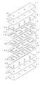
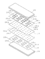
コンピュータなどのOA機器のノイズ除去用などの用途に用いられる電子部品として、セラミック基体の内部に複数のコイル導体を内蔵した積層コイルアレイがある。図10は従来より知られている積層コイルアレイの透視斜視図であり、図11は分解斜視図である。 As an electronic component used for noise removal of OA equipment such as a computer, there is a laminated coil array in which a plurality of coil conductors are built in a ceramic substrate. FIG. 10 is a perspective view of a conventional multilayer coil array, and FIG. 11 is an exploded perspective view.
磁性体セラミックスなどからなるセラミック積層体10はセラミック層14が積層されてなり、セラミック層14にスクリーン印刷などの方法によって形成された内部導体層がビアホール23によって接続されてコイル導体20a〜20dを形成している。セラミック積層体10には、その長手方向に沿って複数のコイル導体20a〜20dが内蔵されている。コイル導体20a〜20dの端部は、ビアホール21を介して、セラミック積層体10の表面に形成された外部電極30a〜30dに接続されている。
The ceramic laminated
この種の積層コイルアレイでは、セラミック積層体10の端面側に配置されたコイル導体20a,20dと、内側に配置されたコイル導体20b,20cとでは、磁路の断面積が異なるため、インダクタンスが異なることが知られている。具体的には、端面側に配置されたコイル導体20a,20dの磁路が狭くなり、内側のコイル導体20b,20cよりもインダクタンスが小さくなる。
In this type of laminated coil array, the coil conductors 20a and 20d arranged on the end face side of the ceramic laminated
そこで、端面側に配置されたコイル導体と内側に配置されたコイル導体とのインダクタンスを等しくするために、端面側に配置されたコイル導体のターン数を、内側に配置されたコイル導体のターン数よりも多くしたり、端面側に配置されたコイル導体の径を内側に配置されたコイル導体の径よりも大きくすることが特許文献1に記載されている。
Therefore, in order to make the inductance of the coil conductor arranged on the end face side equal to that of the coil conductor arranged on the inner side, the number of turns of the coil conductor arranged on the end face side is set to the number of turns of the coil conductor arranged on the inner side.
また、積層コイルアレイではないが、積層コイル部品のインダクタンスを調整するために、セラミック積層体の内部にコイル導体と重なるように浮遊導体を形成し、磁路を狭くすることが特許文献2に記載されている。
特許文献1に記載された発明では、端面側のコイル導体のターン数を多くしたりコイル径を大きくしたりするため、外側のコイル導体のほうが線路長が長くなってしまう。これにより、内側のコイル導体よりも直流抵抗が大きくなってしまうという問題がある。つまり、インダクタンスを等しくすると直流抵抗が異なってしまうことになる。
In the invention described in
特許文献2に記載された発明では、線路長を変化させずに、浮遊導体とコイル導体とが重なる面積を調整することによってインダクタンスを調整するので、直流抵抗を変化させずにインダクタンスを変化させることができる。よって、特許文献2に記載された発明を積層コイルアレイに適用すれば、内側と端面側のコイル導体のインダクタンスと直流抵抗を共に等しくすることができる。
In the invention described in
しかしながら、特許文献2に記載された発明では浮遊導体とコイル導体とが重なっているため、浮遊導体とコイル導体との間に比較的大きな浮遊容量が発生する。浮遊容量が大きくなると自己共振周波数が低下し、周波数の高いノイズの減衰量が低下する。コンピュータなどのOA機器の使用周波数がますます高くなりつつある現在、高周波帯域での良好なノイズ減衰特性が要求されている。
However, in the invention described in
よって、本発明はセラミック積層体の内部に複数のコイル導体が配置された積層コイルアレイにおいて、自己共振周波数を低下させないようにしつつ、内側と端面側のコイル導体のインダクタンスおよび直流抵抗を略等しくすることを目的とする。 Therefore, according to the present invention, in a multilayer coil array in which a plurality of coil conductors are arranged inside a ceramic multilayer body, the inductance and DC resistance of the coil conductors on the inner side and the end face side are made substantially equal while preventing the self-resonant frequency from being lowered. For the purpose.
本発明は上述の問題点を鑑みてなされたものであり、本発明の積層コイルアレイは、複数のセラミック層と内部導体層が交互に積層されてなる積層体を備え、複数の前記内部導体層が直列に接続されてなりコイル軸方向が前記積層体の積層方向に平行であるコイル導体が前記積層体の内部に3個以上配置されている積層コイルアレイであって、前記積層体の前記コイル導体の配列方向の両端部に位置していないコイル導体の近傍に、前記コイル導体と前記積層体の積層方向で重ならないように前記積層体の積層面に平行な調整用導体を設けたことを特徴とする。 The present invention has been made in view of the above-described problems, and the multilayer coil array of the present invention includes a multilayer body in which a plurality of ceramic layers and internal conductor layers are alternately stacked, and the plurality of internal conductor layers. Is a laminated coil array in which three or more coil conductors are connected in series and the coil axial direction is parallel to the lamination direction of the laminate, and the coil of the laminate is provided. An adjustment conductor parallel to the laminated surface of the laminate is provided in the vicinity of the coil conductor that is not located at both ends of the conductor arrangement direction so as not to overlap in the lamination direction of the coil conductor and the laminate. Features.
これにより、調整用導体で渦電流が発生し、渦電流によって発生した磁界が、内側に配置されたコイル導体のインダクタンスを低下させる。また、調整用導体と内部導体層とはともに積層面に平行に、且つ重ならないように配置されているので、調整用導体と内部導体層とは面同士で対向せずに厚みで対向することになるので、内部導体層と調整用導体との間で発生する浮遊容量が低減される。これにより自己共振周波数の低下が防止され、高周波帯域においても十分なノイズ減衰を得ることができる。 As a result, an eddy current is generated in the adjustment conductor, and the magnetic field generated by the eddy current reduces the inductance of the coil conductor disposed inside. In addition, since the adjustment conductor and the inner conductor layer are both arranged parallel to the laminated surface so as not to overlap with each other, the adjustment conductor and the inner conductor layer are opposed to each other in thickness without facing each other. Therefore, stray capacitance generated between the inner conductor layer and the adjustment conductor is reduced. As a result, a decrease in the self-resonant frequency is prevented, and sufficient noise attenuation can be obtained even in the high frequency band.
また、本発明の積層コイルアレイは、前記調整用導体は、前記積層体の両端部に位置していないコイル導体が周回する内側の領域に設けられていることを特徴とする。 In the multilayer coil array of the present invention, the adjustment conductor is provided in an inner region around which a coil conductor that is not located at both ends of the multilayer body circulates.
コイル導体が周回する内側の領域は磁束が集中するため、より小さな調整用導体でもインダクタンスを低下させることができる。調整用導体が小さくなると浮遊容量が低下し、自己共振周波数の低下を抑制できる。 Since the magnetic flux concentrates in the inner region around the coil conductor, the inductance can be reduced even with a smaller adjustment conductor. When the adjustment conductor is reduced, the stray capacitance is reduced, and the reduction of the self-resonance frequency can be suppressed.
さらに、本発明の積層コイルアレイは、複数のセラミック層と内部導体層が交互に積層されてなる積層体を備え、複数の前記内部導体層が直列に接続されてなりコイル軸方向が前記積層体の積層方向に平行であるコイル導体が前記積層体の内部に3個以上配置されている積層コイルアレイであって、前記積層体の積層面に垂直な端面であって、前記積層体の両端部に位置していないコイル導体の近傍に、調整用導体を設けたことを特徴とする。 Furthermore, the multilayer coil array of the present invention includes a multilayer body in which a plurality of ceramic layers and internal conductor layers are alternately stacked, and a plurality of the internal conductor layers are connected in series, and the coil axial direction is the multilayer body. 3 is a laminated coil array in which three or more coil conductors parallel to the laminating direction are arranged inside the laminated body, and are end faces perpendicular to the laminated surface of the laminated body, and both end portions of the laminated body An adjustment conductor is provided in the vicinity of the coil conductor that is not positioned at the position.
これにより、調整用導体で渦電流が発生し、渦電流によって発生した磁束が、内側に配置されたコイル導体のインダクタンスを低下させる。また、調整用導体と内部導体層とは直交するように配置されているので、調整用導体に対して内部導体層は厚みで対向することになり、内部導体層と調整用導体との間で発生する浮遊容量が低減される。これにより自己共振周波数の低下が防止され、高周波帯域においても十分なノイズ減衰を得ることができる。 Thereby, an eddy current is generated in the adjustment conductor, and the magnetic flux generated by the eddy current reduces the inductance of the coil conductor disposed inside. In addition, since the adjustment conductor and the inner conductor layer are arranged so as to be orthogonal to each other, the inner conductor layer is opposed to the adjustment conductor in thickness, and the gap between the inner conductor layer and the adjustment conductor. The generated stray capacitance is reduced. As a result, a decrease in the self-resonant frequency is prevented, and sufficient noise attenuation can be obtained even in the high frequency band.
さらにまた、本発明の積層コイルアレイは、複数のセラミック層が積層されてなる積層体と、前記積層体の内部に積層面に平行に配置された複数の帯状導体からなる内部導体層と、前記積層体の内部に配置されたバイアホールと、を備え、所定の帯状導体の端部と異なる積層面に配置された帯状導体の端部とをバイアホールによって接続してなりコイル軸方向が前記積層体の積層方向と直交する方向であるコイル導体が、前記積層体の内部に3個以上配置されている積層コイルアレイであって、前記積層体のコイル導体の配列方向の両端部に位置していないコイル導体の近傍に、前記コイル導体と前記積層体の積層方向で重ならないように前記積層体の積層面に平行な調整用導体を設けたことを特徴とする。 Furthermore, the laminated coil array of the present invention includes a laminated body in which a plurality of ceramic layers are laminated, an inner conductor layer made up of a plurality of strip conductors arranged in parallel to the laminated surface inside the laminated body, A via hole disposed in the laminated body, and an end of the predetermined strip-shaped conductor is connected to an end of the strip-shaped conductor disposed on a different laminated surface by a via hole, and the coil axial direction is 3 or more coil conductors arranged in a direction perpendicular to the stacking direction of the body are arranged inside the stack, and are positioned at both ends of the coil conductor in the array direction of the stack. An adjustment conductor parallel to the laminated surface of the multilayer body is provided in the vicinity of a coil conductor that does not overlap in the lamination direction of the coil conductor and the multilayer body.
これにより、調整用導体で渦電流が発生し、渦電流によって発生した磁界が、内側に配置されたコイル導体のインダクタンスを低下させる。また、調整用導体と内部導体層とはともに積層面に平行に、且つ重ならないように配置されているので、調整用導体と内部導体層とは面同士で対向せずに厚みで対向することになるので、内部導体層と調整用導体との間で発生する浮遊容量が低減される。これにより自己共振周波数の低下が防止され、高周波帯域においても十分なノイズ減衰を得ることができる。 As a result, an eddy current is generated in the adjustment conductor, and the magnetic field generated by the eddy current reduces the inductance of the coil conductor disposed inside. In addition, since the adjustment conductor and the inner conductor layer are both arranged parallel to the laminated surface so as not to overlap with each other, the adjustment conductor and the inner conductor layer are opposed to each other in thickness without facing each other. Therefore, stray capacitance generated between the inner conductor layer and the adjustment conductor is reduced. As a result, a decrease in the self-resonant frequency is prevented, and sufficient noise attenuation can be obtained even in the high frequency band.
本発明の積層コイルアレイは、前記コイル導体が、前記コイル軸方向に直交する方向に沿って3個以上配列されている場合や、前記コイル導体が、前記コイル軸方向に沿って3個以上配列されている場合を含む。要するに、3個以上のコイル導体が積層体の内部に直列に配列されていればよい。 In the laminated coil array of the present invention, when three or more coil conductors are arranged along a direction orthogonal to the coil axis direction, or three or more coil conductors are arranged along the coil axis direction. Including cases where In short, it is sufficient that three or more coil conductors are arranged in series inside the multilayer body.
また、本発明に係る積層コイルアレイは、前記調整用導体は強磁性体を含んでなるようにしてもよい。 In the multilayer coil array according to the present invention, the adjustment conductor may include a ferromagnetic material.
調整用導体を強磁性体によって構成することにより、調整用導体の単位面積あたりの渦電流によって発生する磁界が大きくなるので、より小さい調整用導体でインダクタンスを低下させることができる。 By configuring the adjustment conductor with a ferromagnetic material, the magnetic field generated by the eddy current per unit area of the adjustment conductor is increased, so that the inductance can be reduced with a smaller adjustment conductor.
また、本発明に係る積層コイルアレイは、前記調整用導体は前記内部導体層と同一の材料からなるようにしてもよい。 In the laminated coil array according to the present invention, the adjustment conductor may be made of the same material as the inner conductor layer.
セラミック積層体を焼成するときの調整用導体の収縮挙動が、セラミックグリーンシートや内部導体層の収縮挙動と大きく異なる場合、セラミック積層体にクラックが生じることがある。よって、調整用導体と内部導体層を同一の材料で構成するようにすれば、セラミック積層体にクラックが生じることを防止できる。 If the shrinkage behavior of the adjusting conductor when firing the ceramic laminate is significantly different from the shrinkage behavior of the ceramic green sheet or the internal conductor layer, cracks may occur in the ceramic laminate. Therefore, if the adjustment conductor and the inner conductor layer are made of the same material, cracks can be prevented from occurring in the ceramic laminate.
以上のように本発明によれば、内部導体層と調整用導体とが面同士で対向することがないので、浮遊容量の発生を抑制することができる。そのため、端面側のコイル導体と内側のコイル導体との直流抵抗とインダクタンスをそろえるとともに、自己共振周波数の低下を防止して高周波帯域でも良好なノイズ減衰特性をもつ積層コイルアレイを得ることができる。 As described above, according to the present invention, since the inner conductor layer and the adjustment conductor do not face each other, generation of stray capacitance can be suppressed. Therefore, it is possible to obtain a laminated coil array having the same DC resistance and inductance as the coil conductors on the end face side and the inner coil conductor, and preventing the decrease of the self-resonance frequency and having good noise attenuation characteristics even in the high frequency band.
以下において、添付図面を参照しつつ本発明を実施するための最良の形態について説明する。 The best mode for carrying out the present invention will be described below with reference to the accompanying drawings.
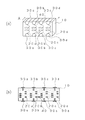
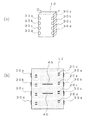
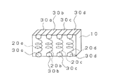
図1(a)は本発明の第1の実施例に係る積層コイルアレイを示す透視斜視図であり、図1(b)はそのA線断面図である。 FIG. 1A is a perspective view showing a laminated coil array according to the first embodiment of the present invention, and FIG.
積層コイルアレイは、磁性体セラミックスからなるセラミック層が積層されてなるセラミック積層体10と、セラミック積層体10に内蔵された4つのコイル導体20a〜20dと、セラミック積層体10の表面に形成された外部電極30a〜30dと、セラミック積層体の内部に配置された調整用導体40とからなる。
The multilayer coil array is formed on the surface of the
コイル導体20a〜20dはコイル軸方向がセラミック積層体10の積層方向と略平行になるように形成されており、4つのコイル導体20a〜20dがコイル軸方向(図の縦方向)に直交する方向に沿って配列されている。また、コイル導体20a〜20dの端部はそれぞれ外部電極30a〜30dに接続されている。4つのコイル導体20a〜20dは、直流抵抗が同一の値となるように、すべて同一の形状とされている。
The coil conductors 20a to 20d are formed so that the coil axis direction is substantially parallel to the lamination direction of the
調整用導体40は、4つのコイル導体20a〜20dのうち端面側に配置されていないもの、すなわち内側に配置されたコイル導体20b,20cの近傍に、セラミック積層体10の積層面と平行に配置されている。
The adjusting
積層コイルアレイでは、すべてのコイル導体20a〜dを同一形状とした場合、端面側に配置されたコイル導体20a,20dの磁路が、内側に配置されたコイル導体20b,20cの磁路より狭くなって、端面側のコイル導体20a,20dのインダクタンスが内側のコイル導体20b,20cよりも低くなる。そこで本発明では、内側のコイル導体20b,20cによって発生する磁束を横切るように、積層面と平行に調整用導体40を配置している。これにより、調整用導体40の内部で渦電流が発生し、渦電流によって発生した磁界が内側のコイル導体20b,20cによって発生する磁界を打ち消すように作用して、内側のコイル導体20b,20cのインダクタンスを低下させる。よって、調整用導体40を適当な大きさにすることによって、端面側のコイル導体20a,20dと内側のコイル導体20b,20cとを同一のインダクタンスにすることができる。
In the laminated coil array, when all the coil conductors 20a to 20d have the same shape, the magnetic paths of the coil conductors 20a and 20d arranged on the end face side are narrower than the magnetic paths of the
調整用導体40は適当な金属から形成されていればよく、金属であれば特に限定されるものではないが、導電性の高い材料や強磁性体が好ましく、具体的にはAgやNiが好適である。調整用導体40を導電性が高い材料や強磁性体で構成することにより、調整用導体40の単位面積あたりの渦電流によって発生する磁束が大きくなるので、調整用導体40の面積を小さくしてもインダクタンス抑制効果を得ることができる。調整用導体40を小さくすれば浮遊容量が減るので、自己共振周波数が高くなって、高周波帯域でのノイズ減衰特性が良好になる。
The
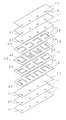
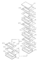
次にこの積層コイルアレイの製造方法について説明する。図3は本発明の第1の実施例に係る積層コイルアレイを示す分解斜視図である。 Next, a method for manufacturing this laminated coil array will be described. FIG. 3 is an exploded perspective view showing the multilayer coil array according to the first embodiment of the present invention.
まず、所定量のFe2O3、NiO、CuO、ZnOなどの金属酸化物を秤量して混合し、仮焼・粉砕を経てNi−Cu−Zn系フェライトの粉末を得る。フェライト粉末、バインダー、可塑剤などを混練してセラミックスラリーを得て、ドクターブレード法などの方法でシート上に成形して無地のセラミックグリーンシートを得る。 First, a predetermined amount of metal oxide such as Fe 2 O 3 , NiO, CuO, ZnO is weighed and mixed, and calcined and pulverized to obtain Ni—Cu—Zn ferrite powder. A ceramic powder is obtained by kneading ferrite powder, a binder, a plasticizer, and the like, and formed on a sheet by a method such as a doctor blade method to obtain a plain ceramic green sheet.
また、Ag粉末、有機ビヒクルなどを混合して導電性ペーストを用意する。導電性ペーストにはAg粉末に加えてPd粉末を含んでいてもよい。また、Ag以外の金属粉末を主成分としてもよいが、導電性を高くして直流抵抗を低減するにはAg粉末が好適である。 Also, a conductive paste is prepared by mixing Ag powder, organic vehicle, and the like. The conductive paste may contain Pd powder in addition to Ag powder. Further, a metal powder other than Ag may be used as a main component, but Ag powder is suitable for increasing conductivity and reducing DC resistance.
次に、この無地のセラミックグリーンシートにレーザ加工装置や金型などを用いて貫通孔を形成し、貫通孔に導電性ペーストを充填してビアホール21を形成し、セラミックグリーンシート11を得る。 Next, through holes are formed in the plain ceramic green sheet using a laser processing apparatus, a mold, or the like, and the via holes 21 are formed by filling the through holes with a conductive paste, whereby the ceramic green sheet 11 is obtained.
また、無地のセラミックグリーンシートに貫通孔を形成し、スクリーン印刷などの方法によって内部導体層22の形成と貫通孔への導電性ペーストの充填を同時に行い、セラミックグリーンシート12を得る。
Moreover, a through-hole is formed in a plain ceramic green sheet, and the formation of the
さらに、無地のセラミックグリーンシートに同様の方法でビアホール23、内部導体層22、調整用導体40を形成してセラミックグリーンシート13を得る。調整用導体40は、セラミックグリーンシート13上に内部導体層22と並んで形成され、セラミックグリーンシート12に形成された内部導体層22ともコイル軸方向に重ならない位置に形成されている。調整用導体40と内部導体層22はともにセラミックグリーンシート13に印刷されているので、セラミック積層体10の積層面(セラミックグリーンシートの面と同じ)と平行になる。よって、調整用導体40と内部導体層22とは面同士で対向することはなく、厚み部分で対向することになる。内部導体層22や調整用導体40の厚みは通常、厚くても20μm程度であるから、調整用導体40と内部導体層22との対向面積は小さく、発生する浮遊容量を小さくすることができる。なお、調整用導体40は異なる積層面に複数設けられていてもよい。
Further, the via
次に、セラミックグリーンシート11〜13を図2に示した所定の順序に積層して焼成し、セラミック積層体10を得る。セラミック積層体10の内部では、内部導体層22がビアホール23を介して直列に接続されてコイル導体20a〜20dを構成する。コイル導体20a〜20dの両端はビアホール21によってセラミック積層体10の表面まで引き出されている。
Next, the ceramic green sheets 11 to 13 are laminated and fired in the predetermined order shown in FIG. Inside the ceramic
セラミック積層体10の表面にAg粉末やガラスを含む導電性ペーストを焼き付け、Niめっき、Snめっきを施して、コイル導体20a〜20dの端部に接続する外部電極30a〜30dを形成し、積層インダクタアレイが完成する。
A conductive paste containing Ag powder and glass is baked on the surface of the
本実施例では調整用導体40はコイル導体20a〜20dと電気的に絶縁された状態に形成されているが、コイル導体20a〜20dと調整用導体40が電気的に接続されているようにしてもよい。ただし、コイル導体20a〜20dと調整用導体40とを電気的に絶縁することにより、調整用導体40で発生した渦電流がコイル導体20a〜20dを通過する電気信号に影響を与えることを防止できるので、コイル導体20a〜20dと調整用導体40とは絶縁されていることが好ましい。
In this embodiment, the
また、上記の実施例ではセラミック材料としてNi−Cu−Zn系フェライトを用いたが、Mn−Zn系フェライトなど他の磁性体材料でもよい。さらに、調整用導体40は内部導体層22と同一の導電性ペーストを用いたが、異なる材料で形成してもよい。その場合、例えばNiなどの強磁性体を好適に用いることができる。調整用導体を強磁性体によって構成することにより、調整用導体の単位面積あたりの渦電流によって発生する磁束が大きくなるので、より小さい調整用導体でインダクタンスを低下させることができる。
In the above embodiment, Ni—Cu—Zn based ferrite is used as the ceramic material, but other magnetic material such as Mn—Zn based ferrite may be used. Furthermore, although the
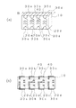
図3(a)は本発明の第2の実施例に係る積層コイルアレイを示す透視斜視図であり、図3(b)はそのB線断面図であり、図4は分解斜視図である。なお、図3および図4においては、図1および図2と共通あるいは対応する部分には同一の符号を付し、適宜説明を省略する。 FIG. 3A is a perspective view showing a laminated coil array according to a second embodiment of the present invention, FIG. 3B is a sectional view taken along line B, and FIG. 4 is an exploded perspective view. 3 and 4, the same reference numerals are given to portions common to or corresponding to those in FIGS. 1 and 2, and description thereof will be omitted as appropriate.
本実施例に係る積層コイルアレイでは、内側のコイル導体20b,20cが周回している内側の領域に、積層面と平行に調整用導体40を配置している。これにより、調整用導体40で渦電流が発生し、内側に配置されたコイル導体20b,20cのインダクタンスを低下させる。
In the laminated coil array according to the present embodiment, the
図4を参照して、この積層コイルアレイの製造方法について説明する。 With reference to FIG. 4, the manufacturing method of this laminated coil array is demonstrated.
Ni−Cu−Zn系フェライトなどの磁性体セラミック材料からなる無地のセラミックグリーンシートを用意し、ビアホール21を形成してセラミックグリーンシート11を得る。また、無地のセラミックグリーンシートに内部導体層22とビアホール23とを形成してセラミックグリーンシート12を得る。さらに、無地のセラミックグリーンシートに内部導体層22と、ビアホール23と、調整用導体40とを形成してセラミックグリーンシート13を得る。
A plain ceramic green sheet made of a magnetic ceramic material such as Ni—Cu—Zn ferrite is prepared, and the via
調整用導体40は、略コ字状の内部導体層22に囲まれた領域に形成されている。すなわち、調整用導体40は、内部導体層22がビアホール23によって接続されてなるコイル導体20b,20cが周回している内側の領域に形成されていて、いずれの内部導体層22ともコイル軸方向に重ならないように形成されている。
The
コイル導体20b,20cが周回している内側の領域には磁束が集中しているため、調整用導体40の単位面積あたりに発生する渦電流が大きくなり、より小さな面積の調整用導体40でインダクタンスを低下させることができる。
Since the magnetic flux is concentrated in the inner region around which the
また、調整用導体40と内部導体層22とが同一面に印刷されていてコイル軸方向に重ならず、面同士が対向しないので、浮遊容量を小さくすることができ、自己共振周波数の低下を防止できる。
Further, since the
セラミックグリーンシート11〜13を図4に示した所定の順序で積層して焼成し、外部電極30a〜30dを形成して積層コイルアレイが完成する。 Ceramic green sheets 11 to 13 are laminated and fired in a predetermined order shown in FIG. 4 to form external electrodes 30a to 30d, thereby completing a laminated coil array.
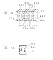
図5(a)は第3の実施例に係る積層コイルアレイを示す透視斜視図であり、図5(b)はそのC線断面図であり、図6は分解斜視図である。なお、図5および図6においては、図1ないし図4と共通あるいは対応する部分には同一の符号を付し、適宜説明を省略する。 FIG. 5A is a perspective view showing a laminated coil array according to the third embodiment, FIG. 5B is a cross-sectional view taken along line C, and FIG. 6 is an exploded perspective view. 5 and 6, the same reference numerals are given to portions common or corresponding to those in FIGS. 1 to 4, and description thereof will be omitted as appropriate.
本実施例に係る積層コイルアレイでは、積層面に垂直なセラミック積層体10の端面であって、内側のコイル導体20b,20cに近接する部分に調整用導体40を形成している。これにより、調整用導体40で渦電流が発生し、内側に配置されたコイル導体20b,20cのインダクタンスを低下させる。
In the laminated coil array according to the present embodiment, the
図6を参照して、この積層コイルアレイの製造方法について説明する。 With reference to FIG. 6, the manufacturing method of this laminated coil array is demonstrated.
Ni−Cu−Zn系フェライトなどの磁性体セラミック材料からなる無地のセラミックグリーンシートを用意し、ビアホール21を形成してセラミックグリーンシート11を得る。また、無地のセラミックグリーンシートに内部導体層22とビアホール23とを形成してセラミックグリーンシート12を得る。
A plain ceramic green sheet made of a magnetic ceramic material such as Ni—Cu—Zn ferrite is prepared, and the via
次に、セラミックグリーンシート11,12を図6に示した所定の順序で積層して焼成してセラミック積層体10を形成する。セラミック積層体10の積層面に対して垂直な端面であって内側のコイル導体20b,20cと近接する部分に調整用導体40を形成する。調整用導体40は導電性ペーストの焼付けやめっき、スパッタ法など適当な方法で形成すればよい。また、焼成前に調整用導体40を形成するようにしてもよい。
Next, the ceramic
コイル導体20b,20cで発生する磁束の多くは、空気よりも透磁率の高いセラミック積層体10の内部を周回するが、磁束の一部はセラミック積層体10の外側に漏れ出して周回している。そのため、セラミック積層体10の表面に調整用導体40を設けることによって、セラミック積層体10の外側に漏れ出している磁束に対して主として作用してコイル導体20b,20cのインダクタンスを低下させる効果がある。
Most of the magnetic flux generated in the
また、コイル導体20a〜dを形成している内部導体層22は積層面に平行に配置されているから、調整用導体40を積層面に対して垂直に配置することにより、内部導体層22と調整用導体40とが面同士で対向することがなく、浮遊容量の発生を抑制することができ、自己共振周波数の低下を防止できる。
Further, since the
次に、セラミック積層体10の表面に導電性ペーストを焼きつけ、Niめっき、Snめっきを施して外部電極30a〜dを形成して積層コイルアレイが完成する。このとき、必要に応じて、調整用導体40にもめっきを施すようにしてもよい。
Next, a conductive paste is baked on the surface of the
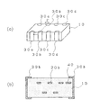
図7(a)は本発明の第4の実施例に係る積層コイルアレイを示す外観斜視図であり、図7(b)はD線断面図であり、図8は分解斜視図である。図7および図8においては、図1ないし図7と共通あるいは対応する部分には同一の符号を付し、適宜説明を省略する。 FIG. 7A is an external perspective view showing a laminated coil array according to a fourth embodiment of the present invention, FIG. 7B is a sectional view taken along the line D, and FIG. 8 is an exploded perspective view. 7 and 8, the same reference numerals are given to portions common or corresponding to those in FIGS.
本実施例に係る積層コイルアレイは、セラミック積層体10の内部に4つのコイル導体20a〜20dが配設されてなる。コイル導体20a〜20dはコイル軸方向に沿ってセラミック積層体10の内部に配列されている。コイル導体20a〜20dの端部はそれぞれ外部電極30a〜30dに接続している。
The laminated coil array according to the present embodiment includes four coil conductors 20 a to 20 d arranged in the ceramic
4つのコイル導体20a〜20dのうち、配列方向の両端部に配置されていないもの、すなわち内側に配置されているコイル導体20b,20cの近傍には、調整用導体40がセラミック積層体10の積層面に平行に配置されている。これにより、コイル導体20b,20cに電流が流れることによって発生する磁束が調整用導体40に作用して渦電流を発生させ、内側に配置されたコイル導体20b,20cのインダクタンスを低下させる。
Of the four coil conductors 20a to 20d, the
図8を参照して、この積層コイルアレイの製造方法について説明する。 With reference to FIG. 8, the manufacturing method of this laminated coil array is demonstrated.
Ni−Cu−Zn系フェライトなどの磁性体セラミック材料からなる無地のセラミックグリーンシートを用意し、内部導体層22およびビアホール23を形成してセラミックグリーンシート12を得る。また、無地のセラミックグリーンシートに内部導体層22、ビアホール23、調整用導体40を形成してセラミックグリーンシート13を得る。調整用導体40は略コ字状の内部導体層22に囲まれた領域に形成されている。すなわち、調整用導体40は内部導体層22がビアホール23によって接続されてなるコイル導体20b,20cが周回している内側の領域に形成されていて、いずれの内部導体層22とも積層方向に重ならないように形成されている。これにより、調整用導体と内部導体層とが面同士で対向しないので、浮遊容量を小さくすることができ、自己共振周波数の低下を防止できる。
A plain ceramic green sheet made of a magnetic ceramic material such as Ni—Cu—Zn ferrite is prepared, and the
セラミックグリーンシート12,13と無地のセラミックグリーンシートを図8に示す所定の順序で積層して焼成し、外部電極30a〜30dを形成して積層コイルアレイが完成する。
The ceramic
図9(a)は本発明の第5の実施例に係る積層コイルアレイを示す外観斜視図であり、図9(b)はE線断面図である。また、図10は分解斜視図である。 FIG. 9A is an external perspective view showing a multilayer coil array according to a fifth embodiment of the present invention, and FIG. 9B is a cross-sectional view taken along line E. FIG. FIG. 10 is an exploded perspective view.
本実施例に係る積層コイルアレイは、磁性体セラッミックスからなる積層体10の内部に4つのコイル導体20a〜20d(コイル導体20a,20c,20dは不図示)を有し、4つのコイル導体20a〜20dの端部はそれぞれ外部電極30a〜30dに接続されている。
The multilayer coil array according to the present embodiment includes four coil conductors 20a to 20d (coil conductors 20a, 20c, and 20d are not shown) inside the
4つのコイル導体20a〜20dはコイル軸方向に直交する方向に配列され、配列方向の両端部に位置していないもの、すなわち内側に配置されているコイル導体20b,20cの近傍には、積層体10の積層面に平行な調整用導体40が形成されている。
The four coil conductors 20a to 20d are arranged in a direction orthogonal to the coil axis direction, and are not positioned at both ends in the arrangement direction, that is, in the vicinity of the
図10を参照してこの積層コイルアレイの製造方法について説明する。 A method for manufacturing this multilayer coil array will be described with reference to FIG.
まず、Ni−Cu−Zn系フェライトなどの磁性体セラミック材料からなる無地のセラミックグリーンシートを用意する。そして無地のセラミックグリーンシートに上部帯状導体24a〜24d、ビアホール26a〜26d、調整用導体40を形成してセラミックグリーンシート16を作製する。調整用導体40は上部帯状導体24a〜24dと同じ積層面に形成されるので、上部帯状導体24a〜24dと調整用導体40とは積層方向に重ならない。つまり上部帯状導体24a〜24dと調整用導体40とが面同士で対向していないので、上部帯状導体24a〜24dと調整用導体40との間に発生する浮遊容量を小さくすることができる。また、無地のセラミックグリーンシートにビアホール26a〜26dを形成してセラミックグリーンシート17を作製する。さらに、無地のセラミックグリーンシートに下部帯状導体25a〜25dを形成してセラミックグリーンシート18を作製する。
First, a plain ceramic green sheet made of a magnetic ceramic material such as Ni—Cu—Zn ferrite is prepared. Then, the upper belt-like conductors 24a to 24d, the via holes 26a to 26d, and the adjusting
次にセラミックグリーンシート16〜18と無地のセラミックグリーンシート17とを図10に示す所定の順序に積層して積層体を得る。すなわち、上部帯状導体24a〜24dが設けられたセラミックグリーンシート16と下部帯状導体25a〜25dが設けられたセラミックグリーンシート18との間には、ビアホール26a〜26dが設けられたセラミックグリーンシート17が配置されている。上部帯状導体24a〜24dの所定の端部と下部帯状導体25a〜25dの所定の端部とがビアホール26a〜26dによって接続されることにより、コイル軸方向が積層体10の積層方向に直交する方向とされたコイル導体20a〜20dが形成される。
Next, the ceramic green sheets 16-18 and the plain ceramic green sheet 17 are laminated | stacked in the predetermined order shown in FIG. 10, and a laminated body is obtained. That is, the ceramic green sheet 17 provided with via holes 26a to 26d is provided between the ceramic
また、上部帯状導体24a〜24d、下部帯状導体25a〜25d、ビアホール26a〜26dによって構成されたコイル導体20a〜20dを積層方向に挟むように無地のセラミックグリーンシート15が積層されている。
A plain ceramic
次にこの積層体10を焼成し、外部電極30を形成して積層コイルアレイが完成する。
Next, this
この積層コイルアレイは、内側に配置されたコイル導体20b,20cの磁束が通過する領域に調整用導体40が配置されているため、調整用導体40に流れる渦電流によって発生する磁束がコイル導体20b,20cのインダクタンスを低下させるので、4つのコイル導体20a〜20dを同一の形状にしても等しいインダクタンスを得ることができる。
In this laminated coil array, since the
なお本実施例においては、調整用導体40を上部帯状電極24a〜24dと同じ積層面に形成したが、異なる積層面に形成してもよい。
In this embodiment, the
本発明は上記の実施例1ないし実施例5に限定されるものではなく、その要旨の範囲内で種々の変更を加えることができる。例えば、磁性体材料や導電性ペーストなどは任意に変更してよい。また、上記の実施例ではいずれも積層体の内部にコイル導体のみが形成されていたが、コイル導体に対して直列あるいは並列にコンデンサが形成されていてもよい。要するに互いに絶縁状態にあるコイル導体が積層体の内部に3つ以上配列されていれば本発明を適用することが可能である。 The present invention is not limited to the first to fifth embodiments described above, and various modifications can be made within the scope of the gist thereof. For example, the magnetic material and the conductive paste may be arbitrarily changed. In each of the above embodiments, only the coil conductor is formed inside the laminate, but a capacitor may be formed in series or in parallel with the coil conductor. In short, the present invention can be applied if three or more coil conductors that are insulated from each other are arranged inside the laminate.
10 セラミック積層体
11,12,13,15,16,17,18 セラミックグリーンシート
14 セラミック層
20a〜20d コイル導体
21,23,26a〜26d ビアホール
22 内部導体層
24a〜24d 上部帯状導体
25a〜25d 下部帯状導体
30a〜30d 外部電極
40 調整用導体
DESCRIPTION OF
Claims (8)
前記積層体の前記コイル導体の配列方向の両端部に位置していないコイル導体の近傍に、前記コイル導体と前記積層体の積層方向で重ならないように前記積層体の積層面に平行な調整用導体を設けたことを特徴とする積層コイルアレイ。 A coil conductor comprising a laminate in which a plurality of ceramic layers and inner conductor layers are alternately laminated, wherein the plurality of inner conductor layers are connected in series, and the coil axis direction is parallel to the lamination direction of the laminate. A laminated coil array in which three or more are arranged inside the laminated body,
For adjustment parallel to the laminate surface of the laminate so that the coil conductor does not overlap in the laminate direction of the laminate in the vicinity of the coil conductor that is not located at both ends of the coil conductor in the arrangement direction of the laminate. A laminated coil array provided with a conductor.
前記積層体の積層面に垂直な端面であって、前記積層体の両端部に位置していないコイル導体の近傍に、調整用導体を設けたことを特徴とする積層コイルアレイ。 A coil conductor comprising a laminate in which a plurality of ceramic layers and inner conductor layers are alternately laminated, wherein the plurality of inner conductor layers are connected in series, and the coil axis direction is parallel to the lamination direction of the laminate. A laminated coil array in which three or more are arranged inside the laminated body,
A laminated coil array, characterized in that an adjustment conductor is provided in the vicinity of a coil conductor that is perpendicular to the laminated surface of the laminated body and is not located at both ends of the laminated body.
前記積層体のコイル導体の配列方向の両端部に位置していないコイル導体の近傍に、前記コイル導体と前記積層体の積層方向で重ならないように前記積層体の積層面に平行な調整用導体を設けたことを特徴とする積層コイルアレイ。 A laminated body in which a plurality of ceramic layers are laminated; an inner conductor layer comprising a plurality of strip-like conductors arranged in parallel to a laminated surface in the laminated body; and a via hole arranged in the laminated body; And a coil whose axial direction is perpendicular to the stacking direction of the multilayer body, wherein the end of the predetermined strip-shaped conductor is connected to the end of the strip-shaped conductor disposed on a different laminated surface by a via hole. A laminated coil array in which three or more conductors are arranged inside the laminated body,
An adjustment conductor parallel to the laminate surface of the laminate so that the coil conductor does not overlap in the laminate direction of the laminate in the vicinity of the coil conductor that is not located at both ends in the arrangement direction of the coil conductors of the laminate. A laminated coil array comprising:
Priority Applications (1)
| Application Number | Priority Date | Filing Date | Title |
|---|---|---|---|
| JP2004109188A JP2005294637A (en) | 2004-04-01 | 2004-04-01 | Laminated coil array |
Applications Claiming Priority (1)
| Application Number | Priority Date | Filing Date | Title |
|---|---|---|---|
| JP2004109188A JP2005294637A (en) | 2004-04-01 | 2004-04-01 | Laminated coil array |
Publications (1)
| Publication Number | Publication Date |
|---|---|
| JP2005294637A true JP2005294637A (en) | 2005-10-20 |
Family
ID=35327211
Family Applications (1)
| Application Number | Title | Priority Date | Filing Date |
|---|---|---|---|
| JP2004109188A Pending JP2005294637A (en) | 2004-04-01 | 2004-04-01 | Laminated coil array |
Country Status (1)
| Country | Link |
|---|---|
| JP (1) | JP2005294637A (en) |
Cited By (5)
| Publication number | Priority date | Publication date | Assignee | Title |
|---|---|---|---|---|
| WO2008013071A1 (en) * | 2006-07-27 | 2008-01-31 | Murata Manufacturing Co., Ltd. | Noise filter array |
| WO2008069022A1 (en) * | 2006-12-08 | 2008-06-12 | Murata Manufacturing Co., Ltd. | Electronic component |
| JP2010245134A (en) * | 2009-04-02 | 2010-10-28 | Murata Mfg Co Ltd | Electronic component and method of manufacturing same |
| CN111986875A (en) * | 2019-05-24 | 2020-11-24 | 株式会社村田制作所 | Laminated coil component |
| WO2021106477A1 (en) * | 2019-11-26 | 2021-06-03 | 株式会社村田製作所 | Laminated coil component |
Citations (9)
| Publication number | Priority date | Publication date | Assignee | Title |
|---|---|---|---|---|
| JPH0463108U (en) * | 1990-10-04 | 1992-05-29 | ||
| JPH04130409U (en) * | 1991-05-17 | 1992-11-30 | 太陽誘電株式会社 | inductance element |
| JPH0766037A (en) * | 1993-08-25 | 1995-03-10 | Tdk Corp | Laminated electronic parts |
| JPH07201568A (en) * | 1993-12-28 | 1995-08-04 | Taiyo Yuden Co Ltd | Laminated chip inductor |
| JPH09186017A (en) * | 1995-12-28 | 1997-07-15 | Tokin Corp | Multilayer inductor and manufacturing method thereof |
| JPH11224817A (en) * | 1998-02-06 | 1999-08-17 | Murata Mfg Co Ltd | Laminated inductor array |
| JP2001110641A (en) * | 1999-10-06 | 2001-04-20 | Tokin Corp | Multi-layer impedance element |
| JP2003217935A (en) * | 2002-01-24 | 2003-07-31 | Murata Mfg Co Ltd | Layered inductor array |
| JP2003272925A (en) * | 2002-03-18 | 2003-09-26 | Mitsubishi Materials Corp | Electronic components |
-
2004
- 2004-04-01 JP JP2004109188A patent/JP2005294637A/en active Pending
Patent Citations (9)
| Publication number | Priority date | Publication date | Assignee | Title |
|---|---|---|---|---|
| JPH0463108U (en) * | 1990-10-04 | 1992-05-29 | ||
| JPH04130409U (en) * | 1991-05-17 | 1992-11-30 | 太陽誘電株式会社 | inductance element |
| JPH0766037A (en) * | 1993-08-25 | 1995-03-10 | Tdk Corp | Laminated electronic parts |
| JPH07201568A (en) * | 1993-12-28 | 1995-08-04 | Taiyo Yuden Co Ltd | Laminated chip inductor |
| JPH09186017A (en) * | 1995-12-28 | 1997-07-15 | Tokin Corp | Multilayer inductor and manufacturing method thereof |
| JPH11224817A (en) * | 1998-02-06 | 1999-08-17 | Murata Mfg Co Ltd | Laminated inductor array |
| JP2001110641A (en) * | 1999-10-06 | 2001-04-20 | Tokin Corp | Multi-layer impedance element |
| JP2003217935A (en) * | 2002-01-24 | 2003-07-31 | Murata Mfg Co Ltd | Layered inductor array |
| JP2003272925A (en) * | 2002-03-18 | 2003-09-26 | Mitsubishi Materials Corp | Electronic components |
Cited By (12)
| Publication number | Priority date | Publication date | Assignee | Title |
|---|---|---|---|---|
| WO2008013071A1 (en) * | 2006-07-27 | 2008-01-31 | Murata Manufacturing Co., Ltd. | Noise filter array |
| US7880564B2 (en) | 2006-07-27 | 2011-02-01 | Murata Manufacturing Co., Ltd. | Noise filter array |
| WO2008069022A1 (en) * | 2006-12-08 | 2008-06-12 | Murata Manufacturing Co., Ltd. | Electronic component |
| JP2010245134A (en) * | 2009-04-02 | 2010-10-28 | Murata Mfg Co Ltd | Electronic component and method of manufacturing same |
| US8193894B2 (en) | 2009-04-02 | 2012-06-05 | Murata Manufacturing Co., Ltd. | Electronic component and method of manufacturing same |
| CN111986875A (en) * | 2019-05-24 | 2020-11-24 | 株式会社村田制作所 | Laminated coil component |
| WO2021106477A1 (en) * | 2019-11-26 | 2021-06-03 | 株式会社村田製作所 | Laminated coil component |
| JPWO2021106477A1 (en) * | 2019-11-26 | 2021-06-03 | ||
| CN114730655A (en) * | 2019-11-26 | 2022-07-08 | 株式会社村田制作所 | Laminated coil component |
| JP7327506B2 (en) | 2019-11-26 | 2023-08-16 | 株式会社村田製作所 | Laminated coil parts |
| CN114730655B (en) * | 2019-11-26 | 2025-03-25 | 株式会社村田制作所 | Laminated coil components |
| US12406800B2 (en) | 2019-11-26 | 2025-09-02 | Murata Manufacturing Co., Ltd. | Multilayer coil component |
Similar Documents
| Publication | Publication Date | Title |
|---|---|---|
| US8334746B2 (en) | Electronic component | |
| US7453344B2 (en) | Multilayer coil component | |
| JP3621300B2 (en) | Multilayer inductor for power circuit | |
| US9251943B2 (en) | Multilayer type inductor and method of manufacturing the same | |
| US6515568B1 (en) | Multilayer component having inductive impedance | |
| CN1910710B (en) | laminated coil | |
| US11087914B2 (en) | Common mode choke coil | |
| CN109585122B (en) | Magnetic coupling type coil component | |
| US6590486B2 (en) | Multilayer inductor | |
| US8395471B2 (en) | Electronic component | |
| WO2011132626A1 (en) | Layered inductor | |
| WO2006073092A1 (en) | Laminated coil | |
| CN100382207C (en) | Laminated coil and production method thereof | |
| JP3545701B2 (en) | Common mode choke | |
| KR20130140410A (en) | Multilayer Chip Electronic Components | |
| JP2000182834A (en) | Laminated inductance element and method of manufacturing the same | |
| JP4479353B2 (en) | Multilayer electronic components | |
| JP2005294637A (en) | Laminated coil array | |
| JP2003217935A (en) | Layered inductor array | |
| JP2009088329A (en) | Coil component | |
| WO2011048873A1 (en) | Multilayer inductor | |
| JP2005259774A (en) | Open magnetic circuit type laminated coil component | |
| JP4400430B2 (en) | Multilayer inductor | |
| JP5617614B2 (en) | Coil built-in board | |
| JP2006351954A (en) | Stacked common mode filter |
Legal Events
| Date | Code | Title | Description |
|---|---|---|---|
| A621 | Written request for application examination |
Free format text: JAPANESE INTERMEDIATE CODE: A621 Effective date: 20070122 |
|
| A977 | Report on retrieval |
Free format text: JAPANESE INTERMEDIATE CODE: A971007 Effective date: 20090908 |
|
| A131 | Notification of reasons for refusal |
Free format text: JAPANESE INTERMEDIATE CODE: A131 Effective date: 20091006 |
|
| A521 | Written amendment |
Free format text: JAPANESE INTERMEDIATE CODE: A523 Effective date: 20091203 |
|
| A02 | Decision of refusal |
Free format text: JAPANESE INTERMEDIATE CODE: A02 Effective date: 20100824 |