EP1562234A2 - Image pick-up apparatus and image pick-up system - Google Patents
Image pick-up apparatus and image pick-up system Download PDFInfo
- Publication number
- EP1562234A2 EP1562234A2 EP05002301A EP05002301A EP1562234A2 EP 1562234 A2 EP1562234 A2 EP 1562234A2 EP 05002301 A EP05002301 A EP 05002301A EP 05002301 A EP05002301 A EP 05002301A EP 1562234 A2 EP1562234 A2 EP 1562234A2
- Authority
- EP
- European Patent Office
- Prior art keywords
- image pick
- lens
- solid
- state image
- center
- Prior art date
- Legal status (The legal status is an assumption and is not a legal conclusion. Google has not performed a legal analysis and makes no representation as to the accuracy of the status listed.)
- Granted
Links
Images






Classifications
-
- H—ELECTRICITY
- H10—SEMICONDUCTOR DEVICES; ELECTRIC SOLID-STATE DEVICES NOT OTHERWISE PROVIDED FOR
- H10F—INORGANIC SEMICONDUCTOR DEVICES SENSITIVE TO INFRARED RADIATION, LIGHT, ELECTROMAGNETIC RADIATION OF SHORTER WAVELENGTH OR CORPUSCULAR RADIATION
- H10F39/00—Integrated devices, or assemblies of multiple devices, comprising at least one element covered by group H10F30/00, e.g. radiation detectors comprising photodiode arrays
- H10F39/011—Manufacture or treatment of image sensors covered by group H10F39/12
- H10F39/024—Manufacture or treatment of image sensors covered by group H10F39/12 of coatings or optical elements
-
- H—ELECTRICITY
- H10—SEMICONDUCTOR DEVICES; ELECTRIC SOLID-STATE DEVICES NOT OTHERWISE PROVIDED FOR
- H10F—INORGANIC SEMICONDUCTOR DEVICES SENSITIVE TO INFRARED RADIATION, LIGHT, ELECTROMAGNETIC RADIATION OF SHORTER WAVELENGTH OR CORPUSCULAR RADIATION
- H10F39/00—Integrated devices, or assemblies of multiple devices, comprising at least one element covered by group H10F30/00, e.g. radiation detectors comprising photodiode arrays
- H10F39/80—Constructional details of image sensors
-
- H—ELECTRICITY
- H10—SEMICONDUCTOR DEVICES; ELECTRIC SOLID-STATE DEVICES NOT OTHERWISE PROVIDED FOR
- H10F—INORGANIC SEMICONDUCTOR DEVICES SENSITIVE TO INFRARED RADIATION, LIGHT, ELECTROMAGNETIC RADIATION OF SHORTER WAVELENGTH OR CORPUSCULAR RADIATION
- H10F39/00—Integrated devices, or assemblies of multiple devices, comprising at least one element covered by group H10F30/00, e.g. radiation detectors comprising photodiode arrays
- H10F39/80—Constructional details of image sensors
- H10F39/806—Optical elements or arrangements associated with the image sensors
- H10F39/8063—Microlenses
-
- H—ELECTRICITY
- H10—SEMICONDUCTOR DEVICES; ELECTRIC SOLID-STATE DEVICES NOT OTHERWISE PROVIDED FOR
- H10F—INORGANIC SEMICONDUCTOR DEVICES SENSITIVE TO INFRARED RADIATION, LIGHT, ELECTROMAGNETIC RADIATION OF SHORTER WAVELENGTH OR CORPUSCULAR RADIATION
- H10F39/00—Integrated devices, or assemblies of multiple devices, comprising at least one element covered by group H10F30/00, e.g. radiation detectors comprising photodiode arrays
- H10F39/80—Constructional details of image sensors
- H10F39/806—Optical elements or arrangements associated with the image sensors
- H10F39/8067—Reflectors
-
- H—ELECTRICITY
- H10—SEMICONDUCTOR DEVICES; ELECTRIC SOLID-STATE DEVICES NOT OTHERWISE PROVIDED FOR
- H10F—INORGANIC SEMICONDUCTOR DEVICES SENSITIVE TO INFRARED RADIATION, LIGHT, ELECTROMAGNETIC RADIATION OF SHORTER WAVELENGTH OR CORPUSCULAR RADIATION
- H10F39/00—Integrated devices, or assemblies of multiple devices, comprising at least one element covered by group H10F30/00, e.g. radiation detectors comprising photodiode arrays
- H10F39/80—Constructional details of image sensors
- H10F39/805—Coatings
- H10F39/8057—Optical shielding
Definitions
- the invention relates to an image pick-up apparatus. More particularly, the invention relates to an image pick-up apparatus in which, on a substrate having a plurality of photoelectric converting areas, a solid-state image pick-up element provided with at least one pattern layer formed by divisional exposure and a lens for inputting light into the plurality of photoelectric converting areas of the solid-state image pick-up element are formed and to an image pick-up system.
- a technique called a divisional exposing technique is used for exposing a pattern of a large area.
- Japanese Patent Application Laid-Open No. H05-006849 (corresponding to U.S.P. Nos. 5561317 and 5731131) can be mentioned.
- Fig. 8 is a diagram for explaining the case where an image pick-up element of a size larger than an exposure area of a reduction projecting apparatus is divided into halves and exposed.
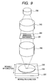
- Fig. 9 is a diagram showing a schematic construction of the reduction projecting apparatus.
- reference numeral 103 denotes an image pick-up element of a size larger than the exposure area of the reduction projecting apparatus; 104 an effective pixel area (pixel area used as data to actually form an image excluding an optical black pixel area or the like); 105R an exposure area of a right reticule; and 105L an exposure area of a left reticule.
- the image pick-up element 103 is formed by joining the exposure areas 105R and 105L and divisionally exposing them.
- a joint line at a joint position of the solid-state image pick-up element (boundary line where patterns are joined in an overlapped portion of the exposure area 105R of the right reticule and the exposure area 105L of the left reticule) is shown.
- a light source 230 passes through a condenser lens 240, a reticule 250, and a projection lens 260 and is projected as pattern light onto a wafer 220 on a stage 200 through a pattern 251 formed on the reticule 250, so that an image pick-up element chip 210 is formed.
- the stage 200 is movable in the X-Y directions.
- the divisional exposure is executed by exchanging the reticule and moving the stage 200.
- the joint position denotes a position where by synthesis of a pattern 1001R' of a first reticule 250R and a pattern 1001L' of a second reticule 250L, a pattern 1001R formed on the substrate (pattern formed by reduction-projecting the pattern 1001R' on the reticule) and a pattern 1001L formed on the substrate (pattern formed by reduction-projecting the pattern 1001L' on the reticule) are joined.
- the joint line denotes a boundary line where the patterns 1001R and 1001L are joined.
- the joint line is not necessarily a straight line. If they are not joined in edge portions of the patterns 1001L' and 1001R' on the reticules but are joined so as to have an overlapped portion, the joint line denotes such an overlapped portion.
- the light enters perpendicularly (shown by arrows of solid lines in the diagram) the pixel P1 and the light enters the pixel P2 in the direction that is inclined from the perpendicular direction (shown by arrows of broken lines in the diagram) by the convergence through the lens as compared with the case of the pixel P1.
- the solid-state image pick-up apparatus is formed by the divisional exposure, if the joint line of the solid-state image pick-up apparatus is located at the center of the optical axis of the lens, the light beam enters perpendicularly the pixel P1 which falls on the joint line and enters a PN junction area. On the other hand, if the joint line of the solid-state image pick-up apparatus is spaced from the center of the optical axis of the lens, the light beam enters the pixel P2 existing on the joint line in the direction inclined from the perpendicular direction.
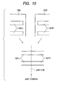
- the exposure could be performed without any displacement to the right or left at the time of the divisional exposure, as shown in Fig. 13, even if the joint line of the solid-state image pick-up apparatus exists at the center of the optical axis of the lens and the light beam enters perpendicularly (shown by the arrows of the solid lines in the diagram) the PN junction area, or even if the joint line of the solid-state image pick-up apparatus is spaced from the center of the optical axis of the lens and the light beam enters the PN junction area in the oblique direction (shown by the arrows of the broken lines in the diagram), the light can enter the PN junction area without being obstructed by wiring patterns 102R and 102L.
- the joint line of the solid-state image pick-up apparatus is spaced from the center of the optical axis of the lens and the light beam enters the PN junction area in the oblique direction (shown by arrows of broken lines in the diagram), a part of the light is obstructed by the wiring pattern 102R and cannot enter the PN junction area.
- the joint position of the solid-state image pick-up apparatus is not made to perfectly coincide with the center of the optical axis of the lens and the output level difference occurs at the joint position, the output level difference of such a degree that it cannot be visually confirmed in the image reproduced by the solid-state image pick-up element can be permitted. Therefore, if the output level difference lies within an allowable range, the joint position of the solid-state image pick-up apparatus and the center of the optical axis of the lens can be spaced from each other.
- a wording "the center of the optical axis of the lens is set onto the approximate joint position where the pattern layers were joined by the divisional exposure" also incorporates the case where the joint position of the solid-state image pick-up apparatus and the center of the optical axis of the lens are spaced from each other in the range where the output level difference is allowable.
- the output level difference cannot be visually confirmed in a range where the output level difference at the joint position does not exceed 1% of an output value at that time and, in this range, the joint position of the solid-state image pick-up apparatus and the center of the optical axis of the lens can be spaced from each other.
- the inventors et al. the output level difference cannot be visually confirmed in a range where the output level difference at the joint position does not exceed 1% of an output value at that time and, in this range, the joint position of the solid-state image pick-up apparatus and the center of the optical axis of the lens can be spaced from each other. According to experiments by the inventors et al.
- a distance between the joint position and the center of the optical axis in the range where the output level difference does not exceed 1% is equal to, for example, 50 mm and to ⁇ 3.6 mm when a lens of an F value of 1.8 is used.
- a lens whose F value is larger than at least 1.8 it is desirable that the joint position coincides with the center of the optical axis in such a range.
- the invention relates to an image pick-up apparatus in which an image pick-up element and a lens for converging the light onto the image pick-up element are provided or a mount to arrange the lens in a position specified by the invention is equipped for an apparatus main body.
- a still camera, a video camera, or the like can be mentioned.
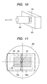
- the still camera as shown in Fig. 10 will be described as an example here.
- Fig. 1 is a diagram showing a layout of a lens and an image pick-up element in the first embodiment of an image pick-up apparatus of the invention.
- reference numeral 103 denotes the image pick-up element in which at least one wiring layer or an impurity injection area of a wafer has been formed by the divisional exposure; 104 the effective pixel area (pixel area used as data to actually form an image excluding an optical black pixel area or the like); 107 a center of the effective pixel area; 105R the exposure range of the right reticule; and 105L the exposure range of the left reticule.
- the joining operation is executed in an overlapped portion of the exposure ranges 105R and 105L.
- a layer where the divisional exposure is executed is assumed to be a wiring layer.
- the wiring layers in a construction of a solid-state image pick-up element having a reset transistor, an amplifying transistor, and a selecting transistor every pixel, a controlling wiring, an output wiring, and the like of each transistor can be given.
- Such wirings can be also allocated to a plurality of wiring layers.
- the controlling wiring of each transistor is allocated as a first layer
- the output wiring is allocated as a second layer
- both layers are formed by the divisional exposure.
- the exposure to form contact holes and through holes for allowing the wiring layers to be come into contact with each other or allowing the substrate and the wirings to be come into contact with each other is also executed by the divisional exposure. Since those layers exert a large influence on the realization of fineness of the pixel and a large aperture ratio, it is preferable to form a fine pattern by the divisional exposure.
- the lens 300 and the image pick-up element 103 are arranged so that the center of the optical axis of the lens 300 (crossing point of an alternate long and short dash line which crosses) is set onto the joint line of the joint position of the image pick-up element 103.
- Reference numeral 106 denotes a center of a chip.
- the lens 300 and the image pick-up element 103 are arranged so that the center of the optical axis of the lens 300 (crossing point of an alternate long and short dash line which crosses) is set onto the joint line of the image pick-up element 103, even if the displacement to the right or left at the time of the divisional exposure occurs, when the joint line of the solid-state image pick-up apparatus coincides with the approximate center of the optical axis of the lens, a change in the light beam which enters a PN junction area 101 is small, so that the output level difference in the case of using the joint line as a boundary, the bright line, the black bar, or the like can be suppressed.
- the joint position can be recognized as coordinates on the chip at the designing stage, to actually allow the joint position to coincide with the center of the optical axis, when the chip is assembled into the camera, it is preferable to position the chip and the lens on the basis of those coordinates and allow the center of the optical axis to coincide with the joint position.
- Fig. 2 is a diagram showing a layout of a lens and an image pick-up element in the second embodiment of an image pick-up apparatus of the invention. Substantially the same component elements as those shown in Fig. 1 are designated by the same reference numerals and their detailed description is omitted here.
- reference numeral 106 denotes the center of the chip and the chip and the lens are arranged so that the center 107 of the effective pixel area and the center of the optical axis of the lens 300 of the image pick-up element overlap on the joint line.
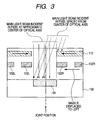
- Fig. 3 is a diagram for explaining the third embodiment of an image pick-up apparatus of the invention.
- Fig. 4 is a diagram showing a layout of a lens and an image pick-up element in the third embodiment of an image pick-up apparatus of the invention. Substantially the same component elements in Figs. 3 and 4 are designated by the same reference numerals and will be explained.
- the output level difference which is caused by mask displacement of the wiring pattern 102 formed by the exposure in a joined fashion can be avoided to a certain degree as shown in Fig. 3 by narrowing a light shielding layer 110 as an upper layer of the wiring pattern 102 so as to have a margin of the light shielding layer 110.
- the joint position shows the joint position between the wiring patterns. Since an amount of the incident light beam is limited by the light shielding layer 110 by narrowing the light shielding layer 110 as shown in Fig. 3, even if the wiring patterns 102R exposed by the right leticule are displaced to the left, its influence is small. However, in the case where the layers over the light shielding layer are formed by the exposure in a joined fashion, it is difficult to avoid the joint displacement by the process for narrowing the light shielding layer 110.
- the joint position in the layers over the light shielding layer is made to coincide with the center of the optical axis of the lens.
- a micro lens layer first lens layer
- an inner lens layer second lens layer
- the inner lens layer is a lens layer which is arranged under the micro lens layer.
- the micro lens layer is formed by patterning a resin and the inner lens layer is obtained by patterning a layer of SiN or the like. The exposure upon the above patterning is executed by the divisional exposure.
- the displacement between the right and left patterns is caused when the joint position at the time of the divisional exposure of micro lens layers 111 is used as a boundary.
- the micro lens layer exposed by the right reticule is now displaced to the left in the diagram, as shown in Fig. 4, if the joint position between the micro lens layers exists at the center of the optical axis of the lens and the light beam enters perpendicularly (shown by arrows of solid lines in Fig. 4) the PN junction area, the light can be converged into the PN junction area even by the micro lens layers with the positional displacement.
- Fig. 5 is a plan view of a pixel in the fourth embodiment of an image pick-up apparatus of the invention and Fig. 6 is a diagram showing a layout of an image pick-up element. Substantially the same component elements in Figs. 5 and 6 are designated by the same reference numerals and will be explained.
- Layer patterns which are arranged in parallel with the joint line remarkably exert an influence of a sensitivity deviation as compared with layer patterns which are perpendicularly arranged.
- a sensitivity deviation As shown in Figs. 5 and 6, if the wiring pattern 102R which is in parallel with the joint line and has been exposed by the right reticule is displaced to the left, a part of the main light beam which has been reflected by the wiring pattern 102R and is incident in the pixel spaced from the center of the optical axis does not enter the PN junction area 101.
- the influence on the wiring patterns which are perpendicularly arranged is small and a ratio of such an influence to causes of the sensitivity deviation of the pixel is small.
- the joint line between, for example, the wiring patterns which are arranged in parallel with the joint line is allowed to coincide with the approximate center of the optical axis of the lens.
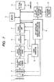
- Fig. 7 is a block diagram showing a "still camera” as an example of a solid-state image pick-up apparatus of the invention.
- reference numeral 1 denotes a barrier functioning as a device to protect the lens and as a main switch; 2 a lens for forming an optical image of an object onto a solid-state image pick-up element 4; 3 a diaphragm for varying an amount of light passing through the lens 2; 4 the solid-state image pick-up element for fetching the object whose image has been formed by the lens 2 as an image signal; 6 an A/D converter for converting the analog image signal that is outputted from the solid-state image pick-up element 4 into a digital signal; 7 a signal processing unit for executing various correcting processes to the image data outputted from the A/D converter 6 or compressing it; 8 a timing generator for generating various timing signals to the solid-state image pick-up element 4, a circuit 5 for processing the image pick-up signal; the A/D converter 6, and the signal processing unit 7; 9 a unit controlling whole structure and arithmetic operation for controlling various arithmetic operations and the whole still video camera; 10 a memory
- a construction in which the lens is integrated and a positional relation among those component elements including the lens is specified in the invention can be used, or a construction having a mount for arranging a lens for exchange so as to obtain the positional relation specified in the invention can be also used.
- a mount is provided as a member for connecting the lens to the solid-state image pick-up apparatus 310 in Fig. 10.
- a main power source is turned on.
- a power source of a control system is subsequently turned on.
- a power source of an image pick-up system circuit such as an A/D converter 6 and the like is turned on.
- the unit controlling whole structure and arithmetic operation 9 opens the diaphragm 3.
- the signal outputted from the solid-state image pick-up element 4 is converted into the A/D converter 6 and, thereafter, inputted to the signal processing unit 7.
- the arithmetic operation of the exposure is executed by the unit controlling whole structure and arithmetic operation 9 on the basis of the data.
- the brightness is discriminated on the basis of a result of the photometric operation.
- the unit controlling whole structure and arithmetic operation 9 controls the diaphragm 3 in accordance with a discrimination result.
- the main exposure is started.
- the image signal outputted from the signal outputted from the solid-state image pick-up element 4 is A/D converted by the A/D converter 6.
- the converted digital signal passes through the signal processing unit 7 and written into the memory 10 by the unit controlling whole structure and arithmetic operation 9.
- the data stored in the memory 10 passes through the I/F unit controlling recording medium 11 under the control of the unit controlling whole structure and arithmetic operation 9 and is recorded onto the detachable recording medium 12 such as a semiconductor memory or the like. It is also possible to construct in such a manner that the data passes through the external I/F unit 13 and is directly inputted to a computer or the like and the image is modified.
- a solid-state image pick-up apparatus in which, on a substrate having a plurality of photoelectric converting areas (photodiodes), a solid-state image pick-up element provided with at least one pattern layer formed by divisional exposure and a lens for introducing light into the plurality of photoelectric converting areas of the solid-state image pick-up element are formed.
Landscapes
- Solid State Image Pick-Up Elements (AREA)
- Transforming Light Signals Into Electric Signals (AREA)
- Studio Devices (AREA)
- Exposure And Positioning Against Photoresist Photosensitive Materials (AREA)
Abstract
Description
Claims (6)
- An image pick-up apparatus comprising, a solid-state image pick-up device comprising at least one pattern layer formed by divisional exposure and a lens for condensing light into said solid-state image pick-up device,
wherein a center of an optical axis of said lens is set to an approximate a portion of joint region between said pattern layers of said divisional exposure. - An apparatus according to claim 1, wherein a center of an effective pixel area comprising a plurality of pixels of said solid-state image pick-up device is set onto said approximate joint region between said pattern layers.
- An apparatus according to claim 1, wherein said solid-state image pick-up device has a light shielding layer and said pattern layers are provided above said light shielding layer.
- An apparatus according to claim 1, wherein said pattern layer is a micro lens layer.
- An apparatus according to claim 1, wherein said pattern layer is a layer arranged almost in parallel with said joint region.
- An image pick-up apparatus comprising a solid-state image pick-up element provided with at least one pattern layer formed by divisional exposure and a mount to fix a lens for introducing light into said plurality of photoelectric converting areas of said solid-state image pick-up element are formed,
wherein a positional relation between said solid-state image pick-up element and said mount is predetermined so that a center of an optical axis of said lens is set to an approximate joint region between said pattern layers of said divisional exposure.
Applications Claiming Priority (2)
| Application Number | Priority Date | Filing Date | Title |
|---|---|---|---|
| JP2004030814A JP3890333B2 (en) | 2004-02-06 | 2004-02-06 | Solid-state imaging device |
| JP2004030814 | 2004-02-06 |
Publications (3)
| Publication Number | Publication Date |
|---|---|
| EP1562234A2 true EP1562234A2 (en) | 2005-08-10 |
| EP1562234A3 EP1562234A3 (en) | 2006-12-13 |
| EP1562234B1 EP1562234B1 (en) | 2012-12-26 |
Family
ID=34675560
Family Applications (1)
| Application Number | Title | Priority Date | Filing Date |
|---|---|---|---|
| EP05002301A Expired - Lifetime EP1562234B1 (en) | 2004-02-06 | 2005-02-03 | Method of manufacturing an image pick-up apparatus |
Country Status (3)
| Country | Link |
|---|---|
| US (2) | US20050174552A1 (en) |
| EP (1) | EP1562234B1 (en) |
| JP (1) | JP3890333B2 (en) |
Families Citing this family (50)
| Publication number | Priority date | Publication date | Assignee | Title |
|---|---|---|---|---|
| JP4508619B2 (en) * | 2003-12-03 | 2010-07-21 | キヤノン株式会社 | Method for manufacturing solid-state imaging device |
| JP3793202B2 (en) * | 2004-02-02 | 2006-07-05 | キヤノン株式会社 | Solid-state imaging device |
| JP4067054B2 (en) * | 2004-02-13 | 2008-03-26 | キヤノン株式会社 | Solid-state imaging device and imaging system |
| US7294818B2 (en) * | 2004-08-24 | 2007-11-13 | Canon Kabushiki Kaisha | Solid state image pickup device and image pickup system comprising it |
| JP2006073736A (en) * | 2004-09-01 | 2006-03-16 | Canon Inc | Photoelectric conversion device, solid-state imaging device, and solid-state imaging system |
| JP4971586B2 (en) * | 2004-09-01 | 2012-07-11 | キヤノン株式会社 | Solid-state imaging device |
| JP5089017B2 (en) * | 2004-09-01 | 2012-12-05 | キヤノン株式会社 | Solid-state imaging device and solid-state imaging system |
| JP4916101B2 (en) * | 2004-09-01 | 2012-04-11 | キヤノン株式会社 | Photoelectric conversion device, solid-state imaging device, and solid-state imaging system |
| JP4459064B2 (en) * | 2005-01-14 | 2010-04-28 | キヤノン株式会社 | Solid-state imaging device, control method thereof, and camera |
| JP4416668B2 (en) * | 2005-01-14 | 2010-02-17 | キヤノン株式会社 | Solid-state imaging device, control method thereof, and camera |
| JP2006197392A (en) * | 2005-01-14 | 2006-07-27 | Canon Inc | Solid-state imaging device, camera, and driving method of solid-state imaging device |
| JP2006237315A (en) * | 2005-02-25 | 2006-09-07 | Matsushita Electric Ind Co Ltd | Solid-state imaging device |
| JP4459099B2 (en) * | 2005-03-18 | 2010-04-28 | キヤノン株式会社 | Solid-state imaging device and camera |
| JP4677258B2 (en) | 2005-03-18 | 2011-04-27 | キヤノン株式会社 | Solid-state imaging device and camera |
| JP4459098B2 (en) | 2005-03-18 | 2010-04-28 | キヤノン株式会社 | Solid-state imaging device and camera |
| JP4794877B2 (en) * | 2005-03-18 | 2011-10-19 | キヤノン株式会社 | Solid-state imaging device and camera |
| JP2007242697A (en) * | 2006-03-06 | 2007-09-20 | Canon Inc | Imaging apparatus and imaging system |
| JP2007273871A (en) * | 2006-03-31 | 2007-10-18 | Toshiba Corp | Design data creation method, design data creation program, and semiconductor device manufacturing method |
| JP4928199B2 (en) * | 2006-09-07 | 2012-05-09 | キヤノン株式会社 | Signal detection device, signal readout method of signal detection device, and imaging system using signal detection device |
| JP4462299B2 (en) | 2007-07-17 | 2010-05-12 | ソニー株式会社 | Imaging apparatus, image processing method, and computer program |
| JP4991436B2 (en) | 2007-08-02 | 2012-08-01 | キヤノン株式会社 | Imaging apparatus and imaging system |
| JP2009141631A (en) * | 2007-12-05 | 2009-06-25 | Canon Inc | Photoelectric conversion device and imaging device |
| JP5268389B2 (en) | 2008-02-28 | 2013-08-21 | キヤノン株式会社 | Solid-state imaging device, driving method thereof, and imaging system |
| JP5173493B2 (en) * | 2008-02-29 | 2013-04-03 | キヤノン株式会社 | Imaging apparatus and imaging system |
| JP5094498B2 (en) | 2008-03-27 | 2012-12-12 | キヤノン株式会社 | Solid-state imaging device and imaging system |
| JP5274166B2 (en) * | 2008-09-10 | 2013-08-28 | キヤノン株式会社 | Photoelectric conversion device and imaging system |
| JP5402092B2 (en) * | 2009-03-04 | 2014-01-29 | ソニー株式会社 | Solid-state imaging device, method for manufacturing solid-state imaging device, and electronic apparatus |
| JP5539105B2 (en) * | 2009-09-24 | 2014-07-02 | キヤノン株式会社 | Photoelectric conversion device and imaging system using the same |
| JP5539104B2 (en) * | 2009-09-24 | 2014-07-02 | キヤノン株式会社 | Photoelectric conversion device and imaging system using the same |
| JP6115982B2 (en) | 2011-07-04 | 2017-04-19 | ソニーセミコンダクタソリューションズ株式会社 | Imaging device and imaging apparatus |
| JP5864990B2 (en) | 2011-10-03 | 2016-02-17 | キヤノン株式会社 | Solid-state imaging device and camera |
| JP5484422B2 (en) | 2011-10-07 | 2014-05-07 | キヤノン株式会社 | Solid-state imaging device |
| JP5967944B2 (en) | 2012-01-18 | 2016-08-10 | キヤノン株式会社 | Solid-state imaging device and camera |
| JP6053505B2 (en) | 2012-01-18 | 2016-12-27 | キヤノン株式会社 | Solid-state imaging device |
| WO2014109044A1 (en) * | 2013-01-11 | 2014-07-17 | ルネサスエレクトロニクス株式会社 | Semiconductor device |
| JP6319946B2 (en) | 2013-04-18 | 2018-05-09 | キヤノン株式会社 | Solid-state imaging device and imaging system |
| JP6100074B2 (en) | 2013-04-25 | 2017-03-22 | キヤノン株式会社 | Photoelectric conversion device and imaging system |
| JP6174901B2 (en) | 2013-05-10 | 2017-08-02 | キヤノン株式会社 | Solid-state imaging device and camera |
| JP5886793B2 (en) * | 2013-06-11 | 2016-03-16 | 浜松ホトニクス株式会社 | Solid-state imaging device |
| JP5886806B2 (en) | 2013-09-17 | 2016-03-16 | キヤノン株式会社 | Solid-state imaging device |
| JP6239975B2 (en) | 2013-12-27 | 2017-11-29 | キヤノン株式会社 | Solid-state imaging device and imaging system using the same |
| JP6412328B2 (en) | 2014-04-01 | 2018-10-24 | キヤノン株式会社 | Solid-state imaging device and camera |
| JP6109125B2 (en) | 2014-08-20 | 2017-04-05 | キヤノン株式会社 | Semiconductor device, solid-state imaging device, and imaging system |
| US9979916B2 (en) | 2014-11-21 | 2018-05-22 | Canon Kabushiki Kaisha | Imaging apparatus and imaging system |
| JP2016201397A (en) * | 2015-04-07 | 2016-12-01 | ソニー株式会社 | Solid-state imaging device and electronic device |
| JP6738200B2 (en) | 2016-05-26 | 2020-08-12 | キヤノン株式会社 | Imaging device |
| US10319765B2 (en) | 2016-07-01 | 2019-06-11 | Canon Kabushiki Kaisha | Imaging device having an effective pixel region, an optical black region and a dummy region each with pixels including a photoelectric converter |
| JP7245014B2 (en) | 2018-09-10 | 2023-03-23 | キヤノン株式会社 | Solid-state imaging device, imaging system, and driving method for solid-state imaging device |
| JP7353752B2 (en) | 2018-12-06 | 2023-10-02 | キヤノン株式会社 | Photoelectric conversion device and imaging system |
| JP7336206B2 (en) | 2019-02-27 | 2023-08-31 | キヤノン株式会社 | Method for manufacturing photoelectric conversion device |
Family Cites Families (34)
| Publication number | Priority date | Publication date | Assignee | Title |
|---|---|---|---|---|
| US5107280A (en) * | 1989-09-12 | 1992-04-21 | Brother Kogyo Kabushiki Kaisha | Divisional exposure apparatus |
| JP2902506B2 (en) | 1990-08-24 | 1999-06-07 | キヤノン株式会社 | Semiconductor device manufacturing method and semiconductor device |
| US5561317A (en) * | 1990-08-24 | 1996-10-01 | Canon Kabushiki Kaisha | Method of manufacturing semiconductor devices |
| JPH04355733A (en) * | 1991-06-03 | 1992-12-09 | Nikon Corp | Camera automatic light control device |
| JP3170847B2 (en) * | 1992-02-14 | 2001-05-28 | キヤノン株式会社 | Solid-state image sensor and optical device using the same |
| JPH0743522A (en) * | 1993-05-28 | 1995-02-14 | Nippon Oil Co Ltd | Method for forming substrate having light-shielding layer, substrate having light-shielding layer, counter electrode substrate for black-and-white display thin film transistor (TFT) array substrate, and black-and-white display liquid crystal display device |
| GB9618717D0 (en) * | 1996-09-07 | 1996-10-16 | Philips Electronics Nv | Image sensor |
| US5948577A (en) * | 1997-06-02 | 1999-09-07 | Canon Kabushiki Kaisha | Color filter substrate, liquid crystal display device using the same and method of manufacturing color filter substrate |
| TW421962B (en) * | 1997-09-29 | 2001-02-11 | Canon Kk | Image sensing device using mos type image sensing elements |
| JPH11261046A (en) * | 1998-03-12 | 1999-09-24 | Canon Inc | Solid-state imaging device |
| JP3571909B2 (en) * | 1998-03-19 | 2004-09-29 | キヤノン株式会社 | Solid-state imaging device and method of manufacturing the same |
| US6665010B1 (en) * | 1998-07-21 | 2003-12-16 | Intel Corporation | Controlling integration times of pixel sensors |
| US6995800B2 (en) * | 2000-01-27 | 2006-02-07 | Canon Kabushiki Kaisha | Image pickup apparatus utilizing a plurality of converging lenses |
| GB0029947D0 (en) * | 2000-12-08 | 2001-01-24 | Sgs Thomson Microelectronics | Solid state image sensors and microlens arrays |
| JP3871194B2 (en) * | 2001-08-02 | 2007-01-24 | 日本ビクター株式会社 | Imaging device |
| JP3728260B2 (en) * | 2002-02-27 | 2005-12-21 | キヤノン株式会社 | Photoelectric conversion device and imaging device |
| EP1341377B1 (en) * | 2002-02-27 | 2018-04-11 | Canon Kabushiki Kaisha | Signal processing device for image pickup apparatus |
| JP2003298040A (en) | 2002-04-05 | 2003-10-17 | Fuji Photo Film Co Ltd | Extension type imaging element and imaging element package |
| JP4115220B2 (en) * | 2002-09-19 | 2008-07-09 | キヤノン株式会社 | Imaging device |
| JP4109944B2 (en) * | 2002-09-20 | 2008-07-02 | キヤノン株式会社 | Method for manufacturing solid-state imaging device |
| JP2004191893A (en) * | 2002-12-13 | 2004-07-08 | Canon Inc | Imaging apparatus |
| KR101006435B1 (en) * | 2003-09-01 | 2011-01-06 | 삼성전자주식회사 | An exposure mask, an exposure apparatus including the same, and a manufacturing method of a display panel for a display device using the same |
| JP4514188B2 (en) * | 2003-11-10 | 2010-07-28 | キヤノン株式会社 | Photoelectric conversion device and imaging device |
| JP4508619B2 (en) * | 2003-12-03 | 2010-07-21 | キヤノン株式会社 | Method for manufacturing solid-state imaging device |
| JP3793202B2 (en) * | 2004-02-02 | 2006-07-05 | キヤノン株式会社 | Solid-state imaging device |
| JP4067054B2 (en) * | 2004-02-13 | 2008-03-26 | キヤノン株式会社 | Solid-state imaging device and imaging system |
| US7294818B2 (en) * | 2004-08-24 | 2007-11-13 | Canon Kabushiki Kaisha | Solid state image pickup device and image pickup system comprising it |
| JP2006073736A (en) * | 2004-09-01 | 2006-03-16 | Canon Inc | Photoelectric conversion device, solid-state imaging device, and solid-state imaging system |
| JP4916101B2 (en) * | 2004-09-01 | 2012-04-11 | キヤノン株式会社 | Photoelectric conversion device, solid-state imaging device, and solid-state imaging system |
| JP5089017B2 (en) * | 2004-09-01 | 2012-12-05 | キヤノン株式会社 | Solid-state imaging device and solid-state imaging system |
| JP4971586B2 (en) * | 2004-09-01 | 2012-07-11 | キヤノン株式会社 | Solid-state imaging device |
| JP4416668B2 (en) * | 2005-01-14 | 2010-02-17 | キヤノン株式会社 | Solid-state imaging device, control method thereof, and camera |
| JP2006197392A (en) * | 2005-01-14 | 2006-07-27 | Canon Inc | Solid-state imaging device, camera, and driving method of solid-state imaging device |
| JP4459064B2 (en) * | 2005-01-14 | 2010-04-28 | キヤノン株式会社 | Solid-state imaging device, control method thereof, and camera |
-
2004
- 2004-02-06 JP JP2004030814A patent/JP3890333B2/en not_active Expired - Fee Related
-
2005
- 2005-02-02 US US11/047,562 patent/US20050174552A1/en not_active Abandoned
- 2005-02-03 EP EP05002301A patent/EP1562234B1/en not_active Expired - Lifetime
-
2011
- 2011-03-21 US US13/052,257 patent/US8643765B2/en not_active Expired - Fee Related
Also Published As
| Publication number | Publication date |
|---|---|
| US20050174552A1 (en) | 2005-08-11 |
| EP1562234B1 (en) | 2012-12-26 |
| US8643765B2 (en) | 2014-02-04 |
| JP3890333B2 (en) | 2007-03-07 |
| EP1562234A3 (en) | 2006-12-13 |
| JP2005223707A (en) | 2005-08-18 |
| US20110169996A1 (en) | 2011-07-14 |
Similar Documents
| Publication | Publication Date | Title |
|---|---|---|
| EP1562234B1 (en) | Method of manufacturing an image pick-up apparatus | |
| US7283305B2 (en) | Solid state image pickup device, method for producing the same, and image pickup system comprising the solid state image pickup device | |
| US7135666B2 (en) | Image pick-up device having well structure and image pick-up system using the image pick-up device | |
| US20110045632A1 (en) | Methods of Manufacturing Solid State Image Pickup Devices | |
| JP5488928B2 (en) | Optical navigation device, input device for data processing unit, and method of controlling a cursor on an image output device | |
| US7978255B2 (en) | Solid-state image sensor and image-capturing device | |
| US7427742B2 (en) | Microlens for use with a solid-state image sensor and a non-telecentric taking lens | |
| US6704051B1 (en) | Photoelectric conversion device correcting aberration of optical system, and solid state image pick-up apparatus and device and camera using photoelectric conversion device | |
| CN101960353A (en) | Focus detection device and imaging device with focus detection device | |
| JP3551437B2 (en) | Solid-state imaging device | |
| JP2016192467A (en) | Semiconductor device | |
| US11387273B2 (en) | Photoelectric conversion device, method of manufacturing photoelectric conversion device, imaging system, and image reading apparatus | |
| US5815607A (en) | Image reading device, and inspection apparatus and exposure apparatus using the device | |
| US20190268543A1 (en) | Image sensor and focus adjustment device | |
| US20100143850A1 (en) | Method of Manufacturing a Semiconductor Device | |
| JP2005183600A (en) | Semiconductor device, solid-state imaging device, amplification type solid-state imaging device, imaging system, mask device, and exposure apparatus | |
| US20050153567A1 (en) | Method of forming patterns | |
| JP2006093417A (en) | Pattern forming method, and manufacturing method for solid image-capturing element using the same | |
| JP2024141009A (en) | Image sensor and image pickup device | |
| JP2022163433A (en) | Imaging element and imaging device | |
| JPS6031109A (en) | Focus detecting device of camera | |
| JP2004128429A (en) | High-function image pickup element |
Legal Events
| Date | Code | Title | Description |
|---|---|---|---|
| PUAI | Public reference made under article 153(3) epc to a published international application that has entered the european phase |
Free format text: ORIGINAL CODE: 0009012 |
|
| AK | Designated contracting states |
Kind code of ref document: A2 Designated state(s): AT BE BG CH CY CZ DE DK EE ES FI FR GB GR HU IE IS IT LI LT LU MC NL PL PT RO SE SI SK TR |
|
| AX | Request for extension of the european patent |
Extension state: AL BA HR LV MK YU |
|
| PUAL | Search report despatched |
Free format text: ORIGINAL CODE: 0009013 |
|
| AK | Designated contracting states |
Kind code of ref document: A3 Designated state(s): AT BE BG CH CY CZ DE DK EE ES FI FR GB GR HU IE IS IT LI LT LU MC NL PL PT RO SE SI SK TR |
|
| AX | Request for extension of the european patent |
Extension state: AL BA HR LV MK YU |
|
| 17P | Request for examination filed |
Effective date: 20070613 |
|
| AKX | Designation fees paid |
Designated state(s): AT BE BG CH CY CZ DE DK EE ES FI FR GB GR HU IE IS IT LI LT LU MC NL PL PT RO SE SI SK TR |
|
| 17Q | First examination report despatched |
Effective date: 20071126 |
|
| RIC1 | Information provided on ipc code assigned before grant |
Ipc: H01L 27/146 20060101AFI20120515BHEP |
|
| GRAP | Despatch of communication of intention to grant a patent |
Free format text: ORIGINAL CODE: EPIDOSNIGR1 |
|
| GRAS | Grant fee paid |
Free format text: ORIGINAL CODE: EPIDOSNIGR3 |
|
| GRAA | (expected) grant |
Free format text: ORIGINAL CODE: 0009210 |
|
| AK | Designated contracting states |
Kind code of ref document: B1 Designated state(s): AT BE BG CH CY CZ DE DK EE ES FI FR GB GR HU IE IS IT LI LT LU MC NL PL PT RO SE SI SK TR |
|
| REG | Reference to a national code |
Ref country code: GB Ref legal event code: FG4D |
|
| REG | Reference to a national code |
Ref country code: CH Ref legal event code: EP |
|
| REG | Reference to a national code |
Ref country code: AT Ref legal event code: REF Ref document number: 590860 Country of ref document: AT Kind code of ref document: T Effective date: 20130115 |
|
| REG | Reference to a national code |
Ref country code: DE Ref legal event code: R096 Ref document number: 602005037555 Country of ref document: DE Effective date: 20130307 |
|
| PG25 | Lapsed in a contracting state [announced via postgrant information from national office to epo] |
Ref country code: SE Free format text: LAPSE BECAUSE OF FAILURE TO SUBMIT A TRANSLATION OF THE DESCRIPTION OR TO PAY THE FEE WITHIN THE PRESCRIBED TIME-LIMIT Effective date: 20121226 Ref country code: FI Free format text: LAPSE BECAUSE OF FAILURE TO SUBMIT A TRANSLATION OF THE DESCRIPTION OR TO PAY THE FEE WITHIN THE PRESCRIBED TIME-LIMIT Effective date: 20121226 Ref country code: LT Free format text: LAPSE BECAUSE OF FAILURE TO SUBMIT A TRANSLATION OF THE DESCRIPTION OR TO PAY THE FEE WITHIN THE PRESCRIBED TIME-LIMIT Effective date: 20121226 |
|
| REG | Reference to a national code |
Ref country code: AT Ref legal event code: MK05 Ref document number: 590860 Country of ref document: AT Kind code of ref document: T Effective date: 20121226 |
|
| REG | Reference to a national code |
Ref country code: LT Ref legal event code: MG4D |
|
| REG | Reference to a national code |
Ref country code: NL Ref legal event code: VDEP Effective date: 20121226 |
|
| PG25 | Lapsed in a contracting state [announced via postgrant information from national office to epo] |
Ref country code: GR Free format text: LAPSE BECAUSE OF FAILURE TO SUBMIT A TRANSLATION OF THE DESCRIPTION OR TO PAY THE FEE WITHIN THE PRESCRIBED TIME-LIMIT Effective date: 20130327 Ref country code: SI Free format text: LAPSE BECAUSE OF FAILURE TO SUBMIT A TRANSLATION OF THE DESCRIPTION OR TO PAY THE FEE WITHIN THE PRESCRIBED TIME-LIMIT Effective date: 20121226 |
|
| PG25 | Lapsed in a contracting state [announced via postgrant information from national office to epo] |
Ref country code: SK Free format text: LAPSE BECAUSE OF FAILURE TO SUBMIT A TRANSLATION OF THE DESCRIPTION OR TO PAY THE FEE WITHIN THE PRESCRIBED TIME-LIMIT Effective date: 20121226 Ref country code: IS Free format text: LAPSE BECAUSE OF FAILURE TO SUBMIT A TRANSLATION OF THE DESCRIPTION OR TO PAY THE FEE WITHIN THE PRESCRIBED TIME-LIMIT Effective date: 20130426 Ref country code: BG Free format text: LAPSE BECAUSE OF FAILURE TO SUBMIT A TRANSLATION OF THE DESCRIPTION OR TO PAY THE FEE WITHIN THE PRESCRIBED TIME-LIMIT Effective date: 20130326 Ref country code: CZ Free format text: LAPSE BECAUSE OF FAILURE TO SUBMIT A TRANSLATION OF THE DESCRIPTION OR TO PAY THE FEE WITHIN THE PRESCRIBED TIME-LIMIT Effective date: 20121226 Ref country code: ES Free format text: LAPSE BECAUSE OF FAILURE TO SUBMIT A TRANSLATION OF THE DESCRIPTION OR TO PAY THE FEE WITHIN THE PRESCRIBED TIME-LIMIT Effective date: 20130406 Ref country code: CY Free format text: LAPSE BECAUSE OF FAILURE TO SUBMIT A TRANSLATION OF THE DESCRIPTION OR TO PAY THE FEE WITHIN THE PRESCRIBED TIME-LIMIT Effective date: 20121226 Ref country code: EE Free format text: LAPSE BECAUSE OF FAILURE TO SUBMIT A TRANSLATION OF THE DESCRIPTION OR TO PAY THE FEE WITHIN THE PRESCRIBED TIME-LIMIT Effective date: 20121226 Ref country code: AT Free format text: LAPSE BECAUSE OF FAILURE TO SUBMIT A TRANSLATION OF THE DESCRIPTION OR TO PAY THE FEE WITHIN THE PRESCRIBED TIME-LIMIT Effective date: 20121226 Ref country code: BE Free format text: LAPSE BECAUSE OF FAILURE TO SUBMIT A TRANSLATION OF THE DESCRIPTION OR TO PAY THE FEE WITHIN THE PRESCRIBED TIME-LIMIT Effective date: 20121226 |
|
| PG25 | Lapsed in a contracting state [announced via postgrant information from national office to epo] |
Ref country code: NL Free format text: LAPSE BECAUSE OF FAILURE TO SUBMIT A TRANSLATION OF THE DESCRIPTION OR TO PAY THE FEE WITHIN THE PRESCRIBED TIME-LIMIT Effective date: 20121226 Ref country code: PL Free format text: LAPSE BECAUSE OF FAILURE TO SUBMIT A TRANSLATION OF THE DESCRIPTION OR TO PAY THE FEE WITHIN THE PRESCRIBED TIME-LIMIT Effective date: 20121226 Ref country code: PT Free format text: LAPSE BECAUSE OF FAILURE TO SUBMIT A TRANSLATION OF THE DESCRIPTION OR TO PAY THE FEE WITHIN THE PRESCRIBED TIME-LIMIT Effective date: 20130426 Ref country code: RO Free format text: LAPSE BECAUSE OF FAILURE TO SUBMIT A TRANSLATION OF THE DESCRIPTION OR TO PAY THE FEE WITHIN THE PRESCRIBED TIME-LIMIT Effective date: 20121226 |
|
| PG25 | Lapsed in a contracting state [announced via postgrant information from national office to epo] |
Ref country code: MC Free format text: LAPSE BECAUSE OF NON-PAYMENT OF DUE FEES Effective date: 20130228 |
|
| REG | Reference to a national code |
Ref country code: CH Ref legal event code: PL |
|
| PG25 | Lapsed in a contracting state [announced via postgrant information from national office to epo] |
Ref country code: CH Free format text: LAPSE BECAUSE OF NON-PAYMENT OF DUE FEES Effective date: 20130228 Ref country code: LI Free format text: LAPSE BECAUSE OF NON-PAYMENT OF DUE FEES Effective date: 20130228 Ref country code: DK Free format text: LAPSE BECAUSE OF FAILURE TO SUBMIT A TRANSLATION OF THE DESCRIPTION OR TO PAY THE FEE WITHIN THE PRESCRIBED TIME-LIMIT Effective date: 20121226 |
|
| PLBE | No opposition filed within time limit |
Free format text: ORIGINAL CODE: 0009261 |
|
| STAA | Information on the status of an ep patent application or granted ep patent |
Free format text: STATUS: NO OPPOSITION FILED WITHIN TIME LIMIT |
|
| REG | Reference to a national code |
Ref country code: FR Ref legal event code: ST Effective date: 20131031 |
|
| 26N | No opposition filed |
Effective date: 20130927 |
|
| REG | Reference to a national code |
Ref country code: IE Ref legal event code: MM4A |
|
| PG25 | Lapsed in a contracting state [announced via postgrant information from national office to epo] |
Ref country code: IT Free format text: LAPSE BECAUSE OF FAILURE TO SUBMIT A TRANSLATION OF THE DESCRIPTION OR TO PAY THE FEE WITHIN THE PRESCRIBED TIME-LIMIT Effective date: 20121226 |
|
| REG | Reference to a national code |
Ref country code: DE Ref legal event code: R097 Ref document number: 602005037555 Country of ref document: DE Effective date: 20130927 |
|
| PG25 | Lapsed in a contracting state [announced via postgrant information from national office to epo] |
Ref country code: IE Free format text: LAPSE BECAUSE OF NON-PAYMENT OF DUE FEES Effective date: 20130203 Ref country code: FR Free format text: LAPSE BECAUSE OF NON-PAYMENT OF DUE FEES Effective date: 20130228 |
|
| PG25 | Lapsed in a contracting state [announced via postgrant information from national office to epo] |
Ref country code: TR Free format text: LAPSE BECAUSE OF FAILURE TO SUBMIT A TRANSLATION OF THE DESCRIPTION OR TO PAY THE FEE WITHIN THE PRESCRIBED TIME-LIMIT Effective date: 20121226 |
|
| PG25 | Lapsed in a contracting state [announced via postgrant information from national office to epo] |
Ref country code: LU Free format text: LAPSE BECAUSE OF NON-PAYMENT OF DUE FEES Effective date: 20130203 Ref country code: HU Free format text: LAPSE BECAUSE OF FAILURE TO SUBMIT A TRANSLATION OF THE DESCRIPTION OR TO PAY THE FEE WITHIN THE PRESCRIBED TIME-LIMIT; INVALID AB INITIO Effective date: 20050203 |
|
| PGFP | Annual fee paid to national office [announced via postgrant information from national office to epo] |
Ref country code: DE Payment date: 20170228 Year of fee payment: 13 |
|
| PGFP | Annual fee paid to national office [announced via postgrant information from national office to epo] |
Ref country code: GB Payment date: 20170227 Year of fee payment: 13 |
|
| REG | Reference to a national code |
Ref country code: DE Ref legal event code: R119 Ref document number: 602005037555 Country of ref document: DE |
|
| GBPC | Gb: european patent ceased through non-payment of renewal fee |
Effective date: 20180203 |
|
| PG25 | Lapsed in a contracting state [announced via postgrant information from national office to epo] |
Ref country code: DE Free format text: LAPSE BECAUSE OF NON-PAYMENT OF DUE FEES Effective date: 20180901 |
|
| PG25 | Lapsed in a contracting state [announced via postgrant information from national office to epo] |
Ref country code: GB Free format text: LAPSE BECAUSE OF NON-PAYMENT OF DUE FEES Effective date: 20180203 |