EP1560235A2 - Electrical multilayer component - Google Patents
Electrical multilayer component Download PDFInfo
- Publication number
- EP1560235A2 EP1560235A2 EP05001704A EP05001704A EP1560235A2 EP 1560235 A2 EP1560235 A2 EP 1560235A2 EP 05001704 A EP05001704 A EP 05001704A EP 05001704 A EP05001704 A EP 05001704A EP 1560235 A2 EP1560235 A2 EP 1560235A2
- Authority
- EP
- European Patent Office
- Prior art keywords
- layers
- layer
- electrode
- electrode layers
- shielding
- Prior art date
- Legal status (The legal status is an assumption and is not a legal conclusion. Google has not performed a legal analysis and makes no representation as to the accuracy of the status listed.)
- Granted
Links
Images


Classifications
-
- H—ELECTRICITY
- H01—ELECTRIC ELEMENTS
- H01G—CAPACITORS; CAPACITORS, RECTIFIERS, DETECTORS, SWITCHING DEVICES OR LIGHT-SENSITIVE DEVICES, OF THE ELECTROLYTIC TYPE
- H01G4/00—Fixed capacitors; Processes of their manufacture
- H01G4/30—Stacked capacitors
-
- H—ELECTRICITY
- H01—ELECTRIC ELEMENTS
- H01G—CAPACITORS; CAPACITORS, RECTIFIERS, DETECTORS, SWITCHING DEVICES OR LIGHT-SENSITIVE DEVICES, OF THE ELECTROLYTIC TYPE
- H01G4/00—Fixed capacitors; Processes of their manufacture
- H01G4/002—Details
- H01G4/005—Electrodes
-
- H—ELECTRICITY
- H01—ELECTRIC ELEMENTS
- H01G—CAPACITORS; CAPACITORS, RECTIFIERS, DETECTORS, SWITCHING DEVICES OR LIGHT-SENSITIVE DEVICES, OF THE ELECTROLYTIC TYPE
- H01G4/00—Fixed capacitors; Processes of their manufacture
- H01G4/002—Details
- H01G4/005—Electrodes
- H01G4/012—Form of non-self-supporting electrodes
Definitions
- the invention relates to an electrical multilayer component with electrode layers and dielectric layers.
- an electrical Multi-layer component known which has a base body and stacked electrode layers of a first one and a second grade through dielectric layers are separated from each other and which at least one Make up capacity.
- the electrode layers are at the Side surfaces of the body contacted to the outside.
- the present invention makes the basic principle exploiting, according to which in an electroceramic Multilayer device several capacitors in a single Basic body can be integrated.
- the individual capacities are formed by opposing electrode layers, between where a dielectric layer is arranged.
- Electrode layers are according to the Present invention prepared by providing a Variety of dielectric layers, for example of Green films, then printing on these green films with a metal-containing paste, wherein the printed area later forms the electrode layer.
- a green sheet coated with several electrode layers are included rectangular shape of the multilayer component the Electrode layers in a plane. It is, however conceivable, the dielectric layers not just above each other stack and then sinter, but the Electrode layers, the dielectric layers any to give other external shape.
- the dielectric layers are, as long as they are still present as a green sheet, very flexible and therefore adaptable to different shapes.
- an electrical multilayer component specified which contains at least two capacitors, which each are formed from opposite Electrode layers and at least one intermediate Dielectric layer. At least two to different Electrode layers belonging to capacitors are included laterally offset from each other.
- a component is advantageous in which between two laterally staggered Electrode layers at least one shielding layer is arranged.
- the different capacitors include a reduced one Have stray capacity.
- each of the two at least offset to each other electrode layers partially or completely overlapped by a shielding layer becomes.
- the lateral displacement of two electrode layers to each other in this context means that the Displacement of one electrode layer relative to the other Electrode layer in the plane of one of the two Electrode layers takes place.
- Laterally staggered Electrode layers are obtained, for example, in which two such layer stack next to each other and in different Arranging heights in the multilayer component.
- a Shielding layer can in particular a turn Electrode layer, that is, that they are part of an im Multi-layer component contained capacitor is.
- the shielding layer as well as the Electrode layer sufficiently good electrical conductive Properties, so that they are used to shield electrostatic Fields is suitable.
- the shielding layer may preferably be in lie on a plane parallel to the staggered one another Electrode layers is.
- each of the two Electrode layers are overlapped by a shielding layer, the decoupling between the two layers even further be improved.
- the two electrode layers can are overlapped by one and the same shielding layer.
- the overlapping of the two electrode layers, the belong to different capacitors, has the advantage that the Component takes up less space at the same capacity.
- the device may be provided that between two electrode layers two Shielding layers are provided, the one another Have overlap.
- This embodiment has the advantage that through the Shielding layers are formed a separate capacity can, on the one hand a defined coupling between the Shielding allows and on the other hand a form additional capacitor present in the component, which can be connected from the outside and used accordingly can be.
- each shielding layer part of or several capacitors. This gives you the advantage that the shielding layers in addition to the decoupling of adjacent electrode layers still another function can take over. By being part of a capacitor, they can add to the capacity of another capacitor in the Component is integrated, contribute.
- a first type of electrode layers is provided contribute substantially only to a first capacitor.
- a second type of electrode layers provided, in turn, essentially only one contribute second capacitor.
- the electrode layers of a Each variety is in the form of each one above the other stacked layers. The so formed piles are laterally offset from each other.
- the concept of lateral displacement of stacks to each other as well interpret as it has already been described above is.
- each electrode layer of the first grade and each Electrode layer of the second kind is at least one Shielding layer arranged. It can be one at a time and act the same shielding layer.
- the shielding layer preferably runs parallel to the Electrode layers.
- This embodiment of the device extends the concept the decoupling of individual electrode layers on all Electrode layers belonging to a capacitance. Thereby can the decoupling between two present in the device Capacitors are further improved.
- each shielding layer to each of the two Contributes capacitors may be provided. This can increase the capacity of both in the component contained capacitors in a simple way and Way, and above all, to save space. Because the Capacity increase happens in this case without that Applying additional electrode layers, but only by using the decoupling of the anyway Capacitors necessary shielding.
- each top electrode layer of the device at its top and their bottom provided with a shielding layer.
- this embodiment may also be advantageous that is, if the other constituents of the Multilayer device are arranged symmetrically, the means that the electrode layers are arranged so that the component with both the bottom and with the Top can be mounted on a circuit board without that there is a difference. In this case, that can Provision of shielding layers at the top and on the lower end of the stacked electrode layers one additional contribution to the security against rotation of the component cause.
- the device In another embodiment of the device have two Capacitors on the same capacity. In this case that is Component designed very homogeneous, that is, it too can be easily trained against rotation, so that Oberund Bottom equal on a circuit board can be mounted.
- those in the component provided capacitors different capacities.
- capacitor ceramic contain are special advantageous properties, for example in terms of Temperature dependence of the dielectric constant.
- capacitor ceramic for example, a ceramic based on barium titanate into consideration. It is particularly possible to use so-called "C0G” ceramics. Such a material would be, for example, (Sm, Ba) NdCiO 3 ceramics.
- the doped barium titanate may contain.
- Z5O or Y5V ceramics formed can be made from a barium zirconium titanate.
- HQM materials come into consideration, which formed are made up of basic masses similar to those of C0G masses.
- Dielectric layers With regard to the material of one or more Dielectric layers, it is also advantageous if a material with voltage-dependent resistance, so one so-called varistor ceramic is included.
- varistor ceramics are particularly considered systems, containing ZnO-Bi or ZnO-Pr.
- Such Dielectric layers have the advantage that they are next to the Capacitor still as another component a varistor in integrate the multilayer component.
- the electrode layers and optionally also for shielding layers For example, silver, palladium, platinum, as well as a Silver-palladium alloy, a silver-platinum alloy or also be used copper or nickel. These materials have the advantage that they have good sintering properties in the Have common sintering with many different ceramics.
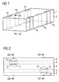
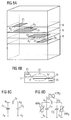
- FIG. 1 shows the main body 6 of a multilayer component in a perspective view.
- the component has a longitudinal axis 7, along which the component extends.
- the main body 6 is cuboid, but may also have any other geometric shape.
- the cuboid shape has the advantage that the component is relatively easy to manufacture and can be used without much additional effort for the SMT (Surface Mount Technology).
- On the side surfaces of the base body 6 outer terminals A 1 , A 2 , A 3 , A 4 are arranged.
- the external connections are applied opposite each other. That is, the outer terminal A 1 is the outer terminal A 4 and the outer terminal A 2 is the outer terminal A 3 opposite.
- the external connections can be made, for example, by burning in a silver stoving paste or other suitable material. They are not only arranged on the side surfaces, but they also surround the base body 6 at its boundary edges and thus cover small parts of the top or the base of the body 6. By this measure, it can be ensured that the device is surface mountable. It can then simply be placed on top or on the bottom of a soldering point and soldered using the Lotddlings the device on a circuit board.
- FIG. 2 shows a longitudinal section through the component Figure 1. It can be seen that the base body 6 is formed is made of superimposed dielectric layers 8.
- This Dielectric layers 8 may, for example, ceramic Green films are in the formable state stacked, pressed, cut and then be sintered so that a monolithic body 6 arises.
- Electrode layers 21, 22, 31, 32 are applied on individual dielectric layers 8 . These Electrode layers are used in the manufacture of the Basic body of the device by imprinting a Screen printing paste or with another suitable Procedure on the still free surface of the concerned Dielectric layer applied. Subsequently, the printed dielectric layers stacked, and as on described above prepared, further processed.
- the electrode layers 21, 22 arranged in the basic body or 31, 32 each form a capacitor 11 or 12.
- the two capacitors are common integrated into the multilayer component. This results the advantage that for the realization of two capacitors consumes less device area on a circuit board is as if the capacitors in individual Multilayer components are present.
- the electrode layers 21, 22 belonging to the capacitor 11 and the electrode layers 31, 32 belonging to the capacitor 12 are laterally offset from one another.
- This lateral offset has been made in the direction of the longitudinal axis 7 of the component and corresponds to the arrangement of the side of the body 6 arranged on the outside terminals A 1 , A 2 , A 3 , A 4th
- the electrode layers 21, 22 are contacted with the external terminals A 1 and A 4 .
- the electrode layers 31, 32 are contacted with the external terminals A 2 and A 3 .
- FIG. 3 shows a section through the component from FIG. 2 along the line III-III.
- the electrode layer 21 is connected to the external terminal A 1 .
- the electrode layer 22 is connected to the external terminal A 4 .
- the electrode layer 21 and the electrode layer 22 overlap one another and thus form a capacitor 11.
- a dielectric layer 8 is arranged between the electrode layers 21, 22.
- the dielectric layers 8 in Figure 2 are all designated by the same reference numeral, this does not mean that these dielectric layers must all be made of the same material. Rather, it is also possible to use 8 different materials for the dielectric layers.
- FIG. 4 shows a section along the line IV-IV from FIG. 2, that is, through the capacitor 12. According to FIG. 3, it can again be seen that the electrode layer 32 is connected to the external terminal A 2 and the electrode layer 31 to the external terminal A 3 .
- FIG. 5 shows the equivalent circuit diagram for the component from FIG. 2. It can be seen here that in the case of the external connection A 1 and A 4, a capacitor with the capacitance C 1 and between the external connection A 2 and A 3 another capacitor with the capacitance C 2 is switched.
- FIG. 6A shows an exemplary embodiment of a component with a shielding layer 41. Otherwise, an electrode layer 21 and an electrode layer 31 are provided in the component. By appropriate marking with A 1 , A 3 and A 4 is indicated with which external terminal the respective electrode layer is contacted in each case. For better clarity, the external connections are not shown even in the perspective view.
- Figure 6A still contains the dielectric layers 8, which are all designated by the same reference numerals, which may well consist of different materials. This may mean, for example, that the uppermost dielectric layer 8 is made of a different material than the subsequent dielectric layer 8.
- FIG. 6B can be seen in a longitudinal section to FIG. 6A, that the electrode layer 21 with the shielding layer 41, which in turn also represents an electrode layer, forms a first capacitor 11.
- the shielding layer 41 is thus Component of each of a capacitor 11, 12 and serves beyond that also the shield between the Electrode layers 21, 31, since now in geometric Regard no more straightforward connection between the Electrode layers 21, 31 is possible without the Shielding layer 41 to cross. This means that electric fields between the electrode layer 21 and the electrode layer 31 produce a possible coupling would be effective through the electrically conductive shielding layer 41 shielded. This will increase the stray capacity effectively reduced between the capacitors 11 and 12.
- FIG. 6A shows that the shielding layer 41 with regard to their shape on the one hand to the electrode layer 21 and on the other hand to the shape of the electrode layer 31 is largely adapted, so that a maximum overlap area to form the respective capacitor 11, 12 is present.
- FIG. 6B exists advantageously an overlap, so that the shielding 41, the electrode layers 21, 31 protrudes laterally. This is However, the figure 6A not apparent.
- FIG. 6C shows an equivalent circuit diagram of the component on FIG. 6A.
- the capacitors 11 and 12 therefore have capacitances C 1 and C 2 and are interconnected in such a way that the terminal A 1 is connected to both capacitors and the terminals A 4 and A 3 are connected only to one of the two capacitors. Starting from the external connection A 1 thus results in a star connection.
- FIG. 7A shows a further embodiment of the component.
- the shielding layer 41 is connected not only to an external terminal but to two external terminals, namely A 2 and A 4 .
- the electrode layers 21 and 31 have an overlap not only with the opposite shielding layer 41 but also with each other.
- FIG. 7B shows that the electrode layer 21 forms two capacitors 11, 12 with the shielding layer 41. This results in particular in conjunction with FIG. 7A.
- a first capacitor is formed over the electrode layer 21, the shielding layer 41 to the outer terminal A 2 and that a second capacitor 12 is formed, starting from the outer terminal A 3 via the electrode layer 21, the shielding 41 to the external connection A 4 .
- This embodiment of the device has the advantage that with three electrode layers four capacitors available can be made.
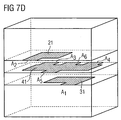
- FIG. 7D shows an extension of the component shown in FIG. 7A.
- the component according to FIG. 7D is designed as a so-called tripod.
- This means that the shielding electrode 41 is connected from one side, from the rear side of the component, to three external terminals.
- the external connections A 4 and A 3 correspond to the external connections shown in FIG.
- an external connection A 6 is shown, which is indicated by dashed lines in Figure 1 and which is arranged between the external terminals A 4 and A 3 . From the opposite side, the shielding layer 41 is made accessible by the external connection A 5 .
- the possibility of contacting the three layers contained in the component is increased.
- FIG. 7D shows the equivalent circuit shown in FIG. 7C.
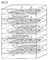
- Figure 7E shows an extension of the embodiment of Figure 7D. Similar to the exemplary embodiment from FIG. 7D, additional external connections A 5 and A 6 are provided in the example according to FIG. 7E. These external connections are shown in FIG. 1 by dashed additional external connections A 5 and A 6 .
- further electrode layers 22, 32 are provided, which can increase the capacitance of the capacitors.
- the electrode layers 21 and 22 are connected to the external terminal A 4 .
- the electrode layers 31 and 32 are connected to the external terminal A 3 .
- shielding layers 41, 42, 43, 44, 45 are provided which are each contacted on the rear side of the component with three external connections A 1 , A 2 and A 5 .
- the shielding layers 41, 42, 43, 44, 45 are contacted with the external terminal A 6 .
- a shielding layer 41, 42, 43, 44, 45 is arranged to form a capacitor, each having an electrode layer.
- a shielding layer 41, 45 is provided at the upper end and at the lower end of the layer stack, which increase the symmetry and improve the shielding of the component towards the outside.
- FIG. 8A shows a further component in a perspective view, wherein two shielding layers are contained.
- the two shielding layers 41 and 51 are different in shape in that they are contacted with different external terminals.
- the shielding layer 41 is contacted with the external terminal A 3 and the shielding layer 51 with the external terminal A 1 . Together with the overlap which the two shielding layers 41, 51 have with each other, this results in the formation of a further capacitor, which can be connected from the outside via the external connections A 1 and A 3 .
- the electrode layer 21 with the shielding layer 41 forms a first capacitor 11.
- the electrode layer 31 forms a further capacitor 13 with the shielding layer 51.
- the two shielding layers 41, 51 also form another one Capacitor 12. As can be seen from the equivalent circuit diagram in FIG. 8C or FIG. 8D, this further capacitor can be connected from the outside.
- the purpose can therefore be achieved, on the one hand, to decouple the two electrode layers 21 and 31 particularly effectively, namely from one another by means of two superimposed shielding layers.
- the two capacitors 11 and 13 receive a defined coupling, which is defined by the capacitance of the capacitor 12.
- a defined coupling is significantly more advantageous in many applications than an undefined stray capacitance between two capacitors arranged in a multilayer component.
- the capacitor 12 representing the defined coupling can be used as noise suppression in an interference suppression circuit.
- FIG. 8B It can still be seen from FIG. 8B that, as in FIGS 6B and 7B, a projection of the shielding layers 41, 51 via the respective electrode layer 21, 31 to be shielded is particularly advantageous.
- FIG. 8C shows a first equivalent circuit diagram for the component from FIG. 8A in the case that only capacitor materials are used for the dielectric layers 8.
- the equivalent circuit consists of three capacitors with capacitances C 1 , C 2 and C 3 .
- the capacitor 12 represented by the capacitance C 2 is accessible from outside through the external connections A 1 and A 2 and can thus be externally connected.
- FIG. 8D Another circuit diagram variant is shown in FIG. 8D. It is assumed here that at least the dielectric layers 8 lying between two electrode layers or between an electrode layer and a shielding layer or between two shielding layers all contain a varistor material. This results in a parallel connection of a voltage-dependent resistor VDR 1 , VDR 2 and VDR 3 to each capacitor C 1 , C 2 , C 3 .
- VDR 1 , VDR 2 and VDR 3 to each capacitor C 1 , C 2 , C 3 .
- two electrode layers with an intervening varistor ceramic form a capacitor on the basis of the electrode layers and the interposed dielectric, and on the other hand a varistor due to the voltage-dependent resistance of the intermediate ceramic layer.
- the two components are connected in parallel, as well as Figure 8D can be seen.
- Such a device equipped with varistor ceramic has the advantage that it can be used as an EMI filter.
- Dielectric layers 8 designed as a varistor material become.
- FIG. 9A shows a further exemplary embodiment of a multilayer component according to the type presented in FIG. 6A, wherein an enlargement can be seen in that yet another capacitor is integrated into the component.
- This is achieved by providing three different types of electrode layers, namely electrode layers 21, 22 and 23. These three electrode layers 21, 22, 23 are contacted with different external connections, A 2 for electrode layer 21, A 4 for electrode layer 22 and A 3 for electrode layer 23.
- the three electrode layers 21, 22, 23 are, as can also be seen in FIG. 9B, each involved in the formation of a capacitor 11, 12, 13. More specifically, the capacitor 13 is formed by the electrode layer 21 and the overlying shielding layer 41. In addition is still involved in the capacitor 13, the underlying shielding layer 42.
- the shielding layers 41, 42, 43 have identical shape and are therefore assigned to the same type of shielding layer. They are all connected to the external connection A 1 .
- the capacitor 12 is formed by the electrode layer 22 and through the shielding layer 41 and through the Shielding layer 43.
- the capacitor 11 is formed by the electrode layer 23 and through the shielding layer 43. Accordingly, the shielding layer 43 and the shielding layer 42 are each involved in two different capacitors.
- the Shielding layer 43 is involved only in the capacitor 13.
- the electrode layer 21st as a counterelectrode for the formation of a capacitor both the shielding layer 42 as well as the uppermost shielding layer 41 is available. So the top one would be Shielding layer 41 for forming a capacitor not absolutely necessary. However, it has the advantage that on the one hand increases the capacitance of the capacitor 13 through it can be, because once again the same capacity comes to as between the electrode layer 21 and the Shielding layer 42 formed capacitance. In addition, has the shielding layer 41 still has the advantage that the Electrode layer 21 is shielded to the outside.
- FIG. 9C shows an equivalent circuit diagram for the component from FIG. 9A, where a star connection of three capacitances C 1 , C 2 , C 3 can be recognized, wherein the external connection A 1 forms the neutral point.
- FIG. 10A shows by way of example how a component formed according to the basic principle of FIG. 8A can be expanded by adding further layers.
- a further electrode layer 32 is now provided.
- this additional electrode layer 32 which is of the same type as the electrode layer 31, that is, that it has the same shape and that it also has the same horizontal position and that it is also connected to the same external terminal, here A 4 .
- the capacitance of one of the capacitors formed in the component can be increased.
- a further shielding layer 52 is accordingly provided in the embodiment according to FIG. 10A in order to ensure good shielding between the electrode layers 31 and 21.
- the shielding layers 41 and 52 again contribute to the capacitor, which contribute between the external terminals A 1 and A 3 , see also FIG. 8C, where the capacitor is designated by the capacitance C 2 .
- the shielding layers 51 and 52 and 53 and 54 in Figure 10A are all of the same type. Likewise, the shielding layers 41 and 42 in Fig. 10A of the same type. For the others Addition of an electrode layer 31 would have the addition the shielding layer 52 is sufficient so that the shielding layers 51 and 54 are not essential for this purpose. They can therefore also be omitted in FIG. 10A.
- a shielding layer as the uppermost layer in the component can have the advantage that the uppermost electrode layer 31 is well shielded not only relative to the electrode layer 21 but also to the outside.
- the shielding layer 51 can also contribute to the capacitance of the capacitor formed with the electrode layer 31, compare the capacitance C 1 in FIG. 8C.
- the capacitor 11 is formed with the participation of Electrode layer 21 and the shielding layers 41 and 42
- the capacitor 12 is formed with the participation of Shielding layers 53 and 42 and the shielding layers 41 and 52
- the capacitor 13 is formed from the Electrode layers 32 and the Abletiken 53 and 54th and the electrode layer 31 and the shield layers 52 and 51.
- the Equivalent circuit diagram according to FIG. 8C is also pointed out.
- FIG. 11A shows by way of example how the basic principle according to FIG. 7A can be extended by adding additional layers.
- the shielding layers 41, 42, 43, 44 and 45 are provided as shielding layers. All of these shielding layers are of the same type, that is to say they are all connected to the outer terminals A 2 and A 4 and otherwise have the same shape and the same horizontal positioning, that is to say that they are identical with respect to the stacking direction.
- the outer shielding layers 41 and 45 serve the Shielding of the device to the outside.
- further electrode and shielding layers here in addition to the electrode layer 21 nor the Electrode layer 22 of the same type comes to it and where with respect to the electrode layer 31 nor the Electrode layer 32 comes of the same type, the Capacity of each capacitor formed here are increased.
- the component shown in FIG. 1 preferably has a base area smaller than 2.5 mm 2 . Particularly advantageous is a footprint of 1.37 mm 2 , which corresponds to the design 0405 and has the advantage that a particularly small component area is required for the two capacitors.
- the Elements described here are also doubled in side by side a single component, which is the number of Increased capacitors and what, for example, in the design 0508 can be realized.
- Figure 8D still shows the advantage in the integration of varistor materials in the dielectric layers, which is evident from the fact that the varistors VDR 1 , VDR 2 and VDR 3 are already integrated in the multilayer component, resulting in separate varistors with a corresponding circuit according to the prior art can be waived.
- the invention is not in terms of number the electrode layers limited. It was shown that here presented concepts arbitrary in the number of Electrode layers can be extended.
Abstract
Description
Die Erfindung betrifft ein elektrisches Vielschichtbauelement mit Elektrodenschichten und Dielektrikumschichten.The invention relates to an electrical multilayer component with electrode layers and dielectric layers.
Aus der Druckschrift DE 100 64 447 C2 ist ein elektrisches Vielschichtbauelement bekannt, das einen Grundkörper aufweist und mit einander verstapelte Elektrodenschichten einer ersten und einer zweiten Sorte die durch Dielektrikumschichten voneinander getrennt sind und welche mindestens eine Kapazität bilden. Die Elektrodenschichten sind dabei an den Seitenflächen des Grundkörpers nach außen hin kontaktiert.From the document DE 100 64 447 C2 is an electrical Multi-layer component known which has a base body and stacked electrode layers of a first one and a second grade through dielectric layers are separated from each other and which at least one Make up capacity. The electrode layers are at the Side surfaces of the body contacted to the outside.
Es ist Aufgabe der vorliegenden Erfindung, ein elektrisches Vielschichtbauelement anzugeben, das verbesserte elektrische Eigenschaften aufweist.It is an object of the present invention to provide an electrical Specify multilayer component, the improved electrical Features.
Die vorliegende Erfindung macht sich das Grundprinzip zunutze, wonach bei einem elektrokeramischen Vielschichtbauelement mehrere Kondensatoren in einen einzigen Grundkörper integriert sein können.The present invention makes the basic principle exploiting, according to which in an electroceramic Multilayer device several capacitors in a single Basic body can be integrated.
Die einzelnen Kapazitäten werden dabei gebildet durch einander gegenüberliegende Elektrodenschichten, zwischen denen eine Dielektrikumschicht angeordnet ist.The individual capacities are formed by opposing electrode layers, between where a dielectric layer is arranged.
Zwischen benachbarten Kondensatoren können Streukapazitäten auftreten, die unerwünscht sind. Die Streukapazitäten resultieren zum einen aus der örtlichen Nähe der die Kondensatoren bildenden Elektrodenschichten. Between adjacent capacitors can be stray capacitances occur that are undesirable. The stray capacities result from the local proximity of the Capacitor-forming electrode layers.
Durch einen vergrößerten Abstand der beiden Elektrodenschichten ergibt sich eine verbesserte Entkopplung, wodurch Streukapazitäten vermindert werden können.Due to an increased distance between the two Electrode layers results in improved decoupling, whereby stray capacitances can be reduced.
Elektrische Vielschichtbauelement werden gemäß der vorliegenden Erfindung hergestellt durch Bereitstellen einer Vielzahl Dielektrikumschichten, beispielsweise von Grünfolien, anschließendem Bedrucken dieser Grünfolien mit einer metallhaltigen Paste, wobei der bedruckte Bereich später die Elektrodenschicht bildet. Wird nun eine Grünfolie mit mehreren Elektrodenschichten beschichtet, so liegen bei rechteckiger Bauform des Vielschichtbauelements die Elektrodenschichten in einer Ebene. Es ist jedoch auch denkbar, die Dielektrikumschichten nicht eben übereinander zu stapeln und anschließend zu sintern, sondern den Elektrodenschichten die Dielektrikumschichten eine beliebige andere äußere Form zu geben. Die Dielektrikumschichten sind, solange sie noch als Grünfolie vorliegen, sehr flexibel und daher an verschiedene Formen anpaßbar.Electrical multilayer components are according to the Present invention prepared by providing a Variety of dielectric layers, for example of Green films, then printing on these green films with a metal-containing paste, wherein the printed area later forms the electrode layer. Will now be a green sheet coated with several electrode layers are included rectangular shape of the multilayer component the Electrode layers in a plane. It is, however conceivable, the dielectric layers not just above each other stack and then sinter, but the Electrode layers, the dielectric layers any to give other external shape. The dielectric layers are, as long as they are still present as a green sheet, very flexible and therefore adaptable to different shapes.
Es wird dementsprechend ein elektrische Vielschichtbauelement angegeben, das mindestens zwei Kondensatoren enthält, welche jeweils gebildet sind aus gegenüberliegenden Elektrodenschichten und wenigstens einer dazwischen liegenden Dielektrikumschicht. Wenigstens zwei zu verschiedenen Kondensatoren gehörende Elektrodenschichten sind dabei seitlich zueinander versetzt.It is accordingly an electrical multilayer component specified, which contains at least two capacitors, which each are formed from opposite Electrode layers and at least one intermediate Dielectric layer. At least two to different Electrode layers belonging to capacitors are included laterally offset from each other.
Es ist darüber hinaus ein Bauelement vorteilhaft, bei dem zwischen zwei seitlich zueinander versetzten Elektrodenschichten wenigstens eine Abschirmschicht angeordnet ist. In addition, a component is advantageous in which between two laterally staggered Electrode layers at least one shielding layer is arranged.
Durch diese besondere Anordnung der Elektrodenschichten kann erreicht werden, daß zwei Elektrodenschichten, die zu verschiedenen Kondensatoren gehören eine verringerte Streukapazität aufweisen.By this particular arrangement of the electrode layers can be achieved that two electrode layers, the different capacitors include a reduced one Have stray capacity.
Es ist darüber hinaus vorteilhaft, wenn jede der beiden zueinander versetzten Elektrodenschichten wenigstens teilweise oder auch ganz von einer Abschirmschicht überlappt wird.It is also beneficial if each of the two at least offset to each other electrode layers partially or completely overlapped by a shielding layer becomes.
Die seitliche Versetzung zweier Elektrodenschichten zueinander bedeutet in diesem Zusammenhang, daß die Versetzung einer Elektrodenschicht relativ zur anderen Elektrodenschicht in der Ebene einer der beiden Elektrodenschichten erfolgt. Üblicherweise liegen Elektrodenschichten, die einen Kondenstor bilden, stapelförmig übereinander. Seitlich zueinander versetzte Elektrodenschichten erhält man beispielsweise in dem man zwei solcher Schichtstapel nebeneinander und in verschiedenen Höhen in dem Vielschichtbauelement anordnet.The lateral displacement of two electrode layers to each other in this context means that the Displacement of one electrode layer relative to the other Electrode layer in the plane of one of the two Electrode layers takes place. Usually lie Electrode layers that form a capacitor, stacked on top of each other. Laterally staggered Electrode layers are obtained, for example, in which two such layer stack next to each other and in different Arranging heights in the multilayer component.
Indem zwischen den Elektrodenschichten eine Abschirmschicht angeordnet ist, kann die kapazitive Entkopplung der beiden Elektrodenschichten noch weiter verbessert werden. Eine Abschirmschicht kann insbesondere ihrerseits eine Elektrodenschicht sein, das heißt, daß sie Teil eines im Vielschichtbauelement enthaltenen Kondensators ist. Darüber hinaus hat natürlich die Abschirmschicht ebenso wie die Elektrodenschicht ausreichend gute elektrische leitfähige Eigenschaften, so daß sie zur Abschirmung elektrostatischer Felder geeignet ist. Die Abschirmschicht kann vorzugsweise in einer Ebene liegen, die parallel zu den zueinander versetzten Elektrodenschichten ist. By providing a shielding layer between the electrode layers is arranged, the capacitive decoupling of the two Electrode layers are further improved. A Shielding layer can in particular a turn Electrode layer, that is, that they are part of an im Multi-layer component contained capacitor is. About that In addition, of course, the shielding layer as well as the Electrode layer sufficiently good electrical conductive Properties, so that they are used to shield electrostatic Fields is suitable. The shielding layer may preferably be in lie on a plane parallel to the staggered one another Electrode layers is.
Darüber hinaus kann dadurch, daß jede der beiden Elektrodenschichten von einer Abschirmschicht überlappt wird, die Entkopplung zwischen den beiden Schichten noch weiter verbessert werden. Die beiden Elektrodenschichten können dabei von ein und derselben Abschirmschicht überlappt werden.In addition, this can be due to the fact that each of the two Electrode layers are overlapped by a shielding layer, the decoupling between the two layers even further be improved. The two electrode layers can are overlapped by one and the same shielding layer.
Mit anderen Worten, es wird dafür Sorge getragen, daß zwei Elektrodenschichten, die in verschiedenen Höhen des Bauelements angeordnet sind, dazwischenliegend noch wenigstens eine Abschirmschicht aufweisen, die die beiden Elektrodenschichten voneinander entkoppelt. Der Überlapp der Abschirmschicht mit einer Elektrodenschicht entkoppelt jede einzelne Elektrodenschicht noch mal für sich in die Richtung, in der die andere Elektrodenschicht liegt. Überlapp bedeutet in diesem Zusammenhang, daß zwei Schichten bei einer Projektion senkrecht zu den Schichtebenen von der einen Schicht auf die andere wenigstens teilweise zur Deckung gelangen.In other words, it will be ensured that two Electrode layers located at different heights of the Component are arranged, in between yet have at least one shielding layer, the two Electrode layers decoupled from each other. The overlap of Shielding layer with an electrode layer decouples each single electrode layer in the direction of in which the other electrode layer is located. Overlapping means in this context, that two layers at a Projection perpendicular to the layer planes of the one Layer on the other at least partially to cover reach.
Darüber hinaus ist es besonders vorteilhaft, wenn bei einem Bauelement zueinander versetzte Elektrodenschichten einander überlappen.In addition, it is particularly advantageous when at a Component offset to each other electrode layers each other overlap.
Das Überlappen der beiden Elektrodenschichten, die zu verschiedenen Kondensatoren gehören, hat den Vorteil, daß das Bauelement bei gleicher Kapazität weniger Platz beansprucht.The overlapping of the two electrode layers, the belong to different capacitors, has the advantage that the Component takes up less space at the same capacity.
In einer anderen Ausführungsform des Bauelementes kann es vorgesehen sein, daß zwischen zwei Elektrodenschichten zwei Abschirmschichten vorgesehen sind, die untereinander einen Überlapp aufweisen. In another embodiment of the device it may be provided that between two electrode layers two Shielding layers are provided, the one another Have overlap.
Darüber hinaus ist es vorteilhaft, wenn zwischen zwei Abschirmschichten mindestens eine Dielektrikumschicht liegt.In addition, it is advantageous if between two Abschirmschichten at least one dielectric layer is located.
Diese Ausführungsform hat den Vorteil, daß durch die Abschirmschichten eine separate Kapazität gebildet werden kann, die einerseits eine definierte Kopplung zwischen den Abschirmschichten ermöglicht und andererseits eine zusätzliche, im Bauelement vorhandenen Kondensator bilden, der von außen beschaltet werden kann und entsprechend genutzt werden kann.This embodiment has the advantage that through the Shielding layers are formed a separate capacity can, on the one hand a defined coupling between the Shielding allows and on the other hand a form additional capacitor present in the component, which can be connected from the outside and used accordingly can be.
In einer anderen Ausführungsform ist es vorgesehen, daß nur eine Abschirmschicht zwischen zwei Elektrodenschichten vorgesehen ist, wobei diese eine Abschirmschicht beide Elektrodenschichten überlappt.In another embodiment it is provided that only a shielding layer between two electrode layers is provided, this one shielding both Electrode layers overlap.
In einer anderen Ausführungsform des Bauelementes kann es vorgesehen sein, daß jede Abschirmschicht Teil eines oder mehrerer Kondensatoren ist. Dadurch wird der Vorteil erzielt, daß die Abschirmschichten neben der Entkopplung von benachbarten Elektrodenschichten noch eine andere Funktion übernehmen können. Indem sie Teil eines Kondensators sind, können sie zur Kapazität eines weiteren Kondensators, der im Bauelement integriert ist, beitragen.In another embodiment of the device it may be provided that each shielding layer part of or several capacitors. This gives you the advantage that the shielding layers in addition to the decoupling of adjacent electrode layers still another function can take over. By being part of a capacitor, they can add to the capacity of another capacitor in the Component is integrated, contribute.
Dadurch kann die Kapazität der im Bauelement vorhandenen Kondensatoren vorteilhaft erhöht werden.This allows the capacity of existing in the device Condensers are advantageously increased.
In einer anderen Ausführungsform des Vielschichtbauelements ist eine erste Sorte von Elektrodenschichten vorgesehen, die im wesentlichen nur zu einem ersten Kondensator beitragen. Darüber hinaus ist eine zweite Sorte von Elektrodenschichten vorgesehen, die ihrerseits im wesentlichen nur zu einem zweiten Kondensator beitragen. Die Elektrodenschichten einer jeden Sorte liegen in Form von jeweils übereinander gestapelten Schichten vor. Die so gebildeten Stapel sind seitlich zueinander versetzt. Hierbei ist der Begriff der seitlichen Versetzung von Stapeln zueinander ebenso zu interpretieren, wie es bereits weiter oben beschrieben worden ist.In another embodiment of the multilayer component For example, a first type of electrode layers is provided contribute substantially only to a first capacitor. In addition, a second type of electrode layers provided, in turn, essentially only one contribute second capacitor. The electrode layers of a Each variety is in the form of each one above the other stacked layers. The so formed piles are laterally offset from each other. Here is the concept of lateral displacement of stacks to each other as well interpret as it has already been described above is.
Zwischen jeder Elektrodenschicht der ersten Sorte und jeder Elektrodenschicht der zweiten Sorte ist wenigstens eine Abschirmschicht angeordnet. Es kann sich dabei jeweils um ein und dieselbe Abschirmschicht handeln.Between each electrode layer of the first grade and each Electrode layer of the second kind is at least one Shielding layer arranged. It can be one at a time and act the same shielding layer.
Die Abschirmschicht verläuft vorzugsweise parallel zu den Elektrodenschichten.The shielding layer preferably runs parallel to the Electrode layers.
Diese Ausführungsform des Bauelements erweitert das Konzept der Entkopplung einzelner Elektrodenschichten auf sämtliche Elektrodenschichten, die einer Kapazität angehören. Dadurch kann die Entkopplung zwischen zwei im Bauelement vorliegenden Kondensatoren noch weiter verbessert werden.This embodiment of the device extends the concept the decoupling of individual electrode layers on all Electrode layers belonging to a capacitance. Thereby can the decoupling between two present in the device Capacitors are further improved.
In einer anderen Ausführungsform des Bauelements kann es vorgesehen sein, daß jede Abschirmschicht zu jedem der beiden Kondensatoren beiträgt. Dadurch kann die Kapazität der beiden im Bauelement enthaltenen Kondensatoren auf einfache Art und Weise und vor allem auch platzsparend erhöht werden. Denn die Kapazitätserhöhung geschieht in diesem Fall ohne das Aufbringen zusätzlicher Elektrodenschichten, sondern lediglich durch Nutzung der ohnehin zur Entkopplung der Kondensatoren notwendigen Abschirmschichten. In another embodiment of the device it may be provided that each shielding layer to each of the two Contributes capacitors. This can increase the capacity of both in the component contained capacitors in a simple way and Way, and above all, to save space. Because the Capacity increase happens in this case without that Applying additional electrode layers, but only by using the decoupling of the anyway Capacitors necessary shielding.
In einer anderen Ausführungsform des Vielschichtbauelements ist die jeweils unterste Elektrodenschicht sowie die jeweils oberste Elektrodenschicht des Bauelements an ihrer Ober- und ihrer Unterseite mit einer Abschirmschicht versehen. Diese Ausführungsform hat den Vorteil, daß die Elektrodenschichten auch nach außen hin gut abgeschirmt werden.In another embodiment of the multilayer component is the lowest electrode layer and each top electrode layer of the device at its top and their bottom provided with a shielding layer. These Embodiment has the advantage that the electrode layers well shielded from the outside.
Darüber hinaus kann diese Ausgestaltung auch von Vorteil sein, wenn nämlich die übrigen Bestandteile des Vielschichtbauelements symmetrisch angeordnet sind, das heißt, daß die Elektrodenschichten so angeordnet sind, daß das Bauelement sowohl mit der Unterseite als auch mit der Oberseite auf eine Leiterplatte montiert werden kann, ohne daß sich ein Unterschied ergibt. In diesem Fall kann das Vorsehen von Abschirmschichten auch am oberen Rand und am unteren Ende der gestapelten Elektrodenschichten einen zusätzlichen Beitrag zur Verdrehsicherheit des Bauelementes bewirken.In addition, this embodiment may also be advantageous that is, if the other constituents of the Multilayer device are arranged symmetrically, the means that the electrode layers are arranged so that the component with both the bottom and with the Top can be mounted on a circuit board without that there is a difference. In this case, that can Provision of shielding layers at the top and on the lower end of the stacked electrode layers one additional contribution to the security against rotation of the component cause.
In einer anderen Ausführungsform des Bauelements weisen zwei Kondensatoren dieselbe Kapazität auf. In diesem Fall ist das Bauelement sehr homogen gestaltet, das heißt, daß es auch leicht verdrehsicher ausgebildet werden kann, so daß Oberund Unterseite gleichberechtigt auf eine Leiterplatte montiert werden können.In another embodiment of the device have two Capacitors on the same capacity. In this case that is Component designed very homogeneous, that is, it too can be easily trained against rotation, so that Oberund Bottom equal on a circuit board can be mounted.
Die Frage der Verdrehsicherheit spielt dabei eine besondere Rolle für den Fall, daß die Bauelemente als SMT-fähige Bauelemente ausgebildet sind. SMT steht dabei für Surface Mount Technologie.The question of security against twisting plays a special role Role in the event that the components as SMT-capable Components are formed. SMT stands for Surface Mount technology.
In einer anderen Ausführungsform haben die im Bauelement vorgesehenen Kondensatoren verschiedene Kapazitäten. In another embodiment, those in the component provided capacitors different capacities.
Hinsichtlich der Dielektrikumschichten ist es besonders vorteilhaft, wenn diese eine sogenannte Kondensatorkeramik enthalten. Diese Kondensatorkeramiken haben besonders vorteilhafte Eigenschaften, beispielsweise hinsichtlich der Temperaturabhängigkeit der Dielektrizitätskonstante.With regard to the dielectric layers, it is particularly advantageous if this is a so-called capacitor ceramic contain. These capacitor ceramics are special advantageous properties, for example in terms of Temperature dependence of the dielectric constant.
Als Kondensatorkeramik kann beispielsweise eine Keramik auf der Basis Bariumtitanat in Betracht kommen. Es kommt insbesondere in Betracht, sogenannte "C0G"-Keramiken zu verwenden. Ein solches Material wäre beispielsweise (Sm, Ba) NdCiO3-Keramik.As a capacitor ceramic, for example, a ceramic based on barium titanate into consideration. It is particularly possible to use so-called "C0G" ceramics. Such a material would be, for example, (Sm, Ba) NdCiO 3 ceramics.
Darüber hinaus kommt aber auch eine sogenannte "X7R"-Keramik in Betracht, die beispielsweise dotiertes Bariumtitanat enthalten kann.In addition, however, comes a so-called "X7R" ceramic for example, the doped barium titanate may contain.
Es kommen darüber hinaus auch weitere Keramikmaterialien in Betracht, beispielsweise Z5O oder Y5V-Keramiken, die gebildet sein können aus einem Barium-Zirkon-Titanat. Darüber hinaus kommen auch HQM-Materialien in Betracht, welche gebildet werden aus Grundmassen, die denen von C0G-Massen gleichen.In addition, there are also other ceramic materials in Consider, for example, Z5O or Y5V ceramics formed can be made from a barium zirconium titanate. Furthermore also HQM materials come into consideration, which formed are made up of basic masses similar to those of C0G masses.
Die genannten Kondensatormaterialien sind insbesondere geeignet für Filter gegenüber elektromagnetischen Störungen (englisch: EMI = "Electro Magnetic Interference"-Filter oder auch rfi = "Radio Frequency Interference"-Filter).The aforementioned capacitor materials are in particular suitable for filters against electromagnetic interference (English: EMI = "Electro Magnetic Interference" filter or also rfi = "Radio Frequency Interference" filter).
Hinsichtlich des Materials einer oder mehrerer Dielektrikumschichten ist es darüber hinaus vorteilhaft, wenn ein Material mit spannungsabhängigem Widerstand, also eine sogenannte Varistorkeramik enthalten ist. Als Varistorkeramiken kommen insbesondere Systeme in Betracht, die ZnO-Bi oder ZnO-Pr enthalten. Solche Dielektrikumschichten haben den Vorteil, daß sie neben dem Kondensator noch als weiteres Bauelement einen Varistor in das Vielschichtbauelement integrieren.With regard to the material of one or more Dielectric layers, it is also advantageous if a material with voltage-dependent resistance, so one so-called varistor ceramic is included. When Varistor ceramics are particularly considered systems, containing ZnO-Bi or ZnO-Pr. Such Dielectric layers have the advantage that they are next to the Capacitor still as another component a varistor in integrate the multilayer component.
Keramikmaterialien mit Varistoreffekt sind dementsprechend vor allem dazu geeignet, ESD (ESD englisch: ESD = "Electro Static Discharge")-Schutzbauelemente herzustellen.Ceramic materials with varistor effect are accordingly especially suitable for ESD (ESD English: ESD = "Electro Static Discharge ") - to produce protective components.
In einer anderen Ausführungsform des Bauelements ist es vorteilhaft, wenn als Material für die Elektrodenschichten sowie gegebenenfalls auch für Abschirmschichten beispielsweise Silber, Palladium, Platin, sowie auch eine Silber-Palladium-Legierung, eine Silber-Platin-Legierung oder auch Kupfer oder Nickel verwendet werden. Diese Materialien haben den Vorteil, daß sie gute Sintereigenschaften bei der Gemeinsamsinterung mit vielen verschiedenen Keramiken haben.In another embodiment of the device it is advantageous if as a material for the electrode layers and optionally also for shielding layers For example, silver, palladium, platinum, as well as a Silver-palladium alloy, a silver-platinum alloy or also be used copper or nickel. These materials have the advantage that they have good sintering properties in the Have common sintering with many different ceramics.
Im folgenden wird die Erfindung anhand von Ausführungsbeispiele und den dazugehörigen Figuren näher erläutert.
Figur 1- zeigt ein Vielschichtbauelement in einer perspektivischen Ansicht mit Außenanschlüssen.
- Figur 2
- zeigt einen Schnitt entlang der Linie II-
II aus Figur 1, also einen Längsschnitt durch dasBauelement aus Figur 1. - Figur 3
- zeigt einen Schnitt entlang der Linie III-III in
Figur 2, also einen Querschnitt durch das
Bauelement aus Figur 1. - Figur 4
- zeigt einen Schnitt entlang der Linie IV-IV in Figur
2, also einen Querschnitt durch das
Bauelement aus Figur 1. - Figur 5
- zeigt ein Ersatzschaltbild für das
Bauelement aus Figur 1. - Figuren 6A, 7A, 8A, 9A, 10A, 11A
- zeigen beispielhafte weitere Vielschichtbauelemente in perspektivischen Ansichten.
- Die Figuren 6B, 7B, 8B, 9B, 10B, 11B
- zeigen Längsschnitte
durch die entsprechenden Vielschichtbauelemente,
wobei die Schnittansichten denen aus Figur 2 in
Bezug auf Figur 1 entsprechen, also wieder Schnittansichten durch die Linie II-II sind. - Die Figuren 6C, 7C, 8C, 9C
- zeigen die zu
den entsprechenden Figuren - Figur 8D
- zeigt ein weiteres Ersatzschaltbild zusätzlich zur
Figur 8C, das man erhält, wenn man in Figur
8A die Dielektrikumschichten 8 so ausführt, daß sie eine Varistorkeramik enthalten. - Figur 7D
- zeigt eine Erweiterung des Bauelements aus Figur 7A.
- Figur 7E
- zeigt eine Erweiterung des Bauelements aus Figur 7D.
- FIG. 1
- shows a multilayer component in a perspective view with external connections.
- FIG. 2
- shows a section along the line II-II of Figure 1, that is, a longitudinal section through the device of Figure 1.
- FIG. 3
- shows a section along the line III-III in Figure 2, that is, a cross section through the device of Figure 1.
- FIG. 4
- shows a section along the line IV-IV in Figure 2, that is, a cross section through the device of Figure 1.
- FIG. 5
- shows an equivalent circuit diagram for the device of Figure 1.
- Figures 6A, 7A, 8A, 9A, 10A, 11A
- show exemplary further multilayer components in perspective views.
- Figures 6B, 7B, 8B, 9B, 10B, 11B
- show longitudinal sections through the corresponding multilayer components, wherein the sectional views correspond to those of Figure 2 with respect to Figure 1, that are again sectional views through the line II-II.
- Figures 6C, 7C, 8C, 9C
- show the corresponding to the corresponding figures 6, 7, 8, 9 equivalent circuit diagrams.
- Figure 8D
- FIG. 8 shows a further equivalent circuit diagram in addition to FIG. 8C, which is obtained when, in FIG. 8A, the
dielectric layers 8 are designed such that they contain a varistor ceramic. - Figure 7D
- shows an extension of the device of Figure 7A.
- Figure 7E
- shows an extension of the device of Figure 7D.
Figur 1 zeigt den Grundkörper 6 eines Vielschichtbauelements
in einer perspektivischen Ansicht.FIG. 1 shows the
Das Bauelement weist eine Längsachse 7 auf, entlang derer
sich das Bauelement erstreckt. Der Grundkörper 6 ist
quaderförmig, kann aber auch jede beliebige andere
geometrische Form aufweisen. Die Quaderform hat den Vorteil,
daß das Bauelement relativ leicht herstellbar ist und auch
ohne größeren Zusatzaufwand für die SMT (Surface Mount
Technologie) verwendet werden kann. Auf den Seitenflächen des
Grundkörpers 6 sind Außenanschlüsse A1, A2, A3, A4
angeordnet.The component has a
Die Außenanschlüsse sind jeweils gegenüberliegend
aufgebracht. Das heißt, dem Außenanschluß A1 liegt der
Außenanschluß A4 und dem Außenanschluß A2 liegt der
Außenanschluß A3 gegenüber. Die Außenanschlüsse können
beispielsweise durch Einbrennen einer Silbereinbrennpaste
oder eines anderen geeigneten Materials hergestellt werden.
Sie sind nicht nur auf den Seitenflächen angeordnet, sondern
sie umgreifen den Grundkörper 6 auch an seinen
Begrenzungskanten und bedecken folglich kleine Teile der
Oberseite beziehungsweise der Grundfläche des Grundkörpers 6.
Durch diese Maßnahme kann sichergestellt werden, daß das
Bauelement oberflächenmontagefähig ist. Es kann dann einfach
auf der Oberseite oder auf der Unterseite ein Lotpunkt
gesetzt werden und mit Hilfe des Lotpunkts das Bauelement auf
einer Leiterplatte verlötet werden.The external connections are applied opposite each other. That is, the outer terminal A 1 is the outer terminal A 4 and the outer terminal A 2 is the outer terminal A 3 opposite. The external connections can be made, for example, by burning in a silver stoving paste or other suitable material. They are not only arranged on the side surfaces, but they also surround the
Figur 2 zeigte einen Längsschnitt durch das Bauelement aus
Figur 1. Es ist zu erkennen, daß der Grundkörper 6 gebildet
ist aus übereinanderliegenden Dielektrikumschichten 8. Diese
Dielektrikumschichten 8 können beispielsweise keramische
Grünfolien sein, die im verformfähigen Zustand
übereinandergestapelt, verpreßt, geschnitten und anschließend
versintert werden, so daß ein monolithischer Grundkörper 6
entsteht. Auf einzelne Dielektrikumschichten 8 sind
Elektrodenschichten 21, 22, 31, 32 aufgebracht. Diese
Elektrodenschichten werden bei der Herstellung des
Grundkörpers des Bauelementes durch Aufdrucken einer
Siebdruckpaste oder auch mit einem anderen geeigneten
Verfahren auf die noch freie Oberfläche der betreffenden
Dielektrikumschicht aufgebracht. Anschließend werden die
bedruckten Dielektrikumschichten verstapelt, und wie weiter
oben bereites beschrieben, weiterverarbeitet.FIG. 2 shows a longitudinal section through the component
Figure 1. It can be seen that the
Dieser grundsätzliche Aufbau des Vielschichtbauelementes ist für alle hier beschriebenen Beispiele der gleiche, allerdings ist dieser Aufbau nicht zwingend und soll keinesfalls als Begrenzung des Schutzbereichs verstanden werden.This basic structure of the multilayer component is for all examples described here the same, however This structure is not mandatory and should not be considered as Limitation of the scope.
Die in dem Grundkörper angeordnete Elektrodenschichten 21, 22
beziehungsweise 31, 32 bilden jeweils eine Kondensator 11
beziehungsweise 12. Die beiden Kondensatoren sind gemeinsam
in das Vielschichtbauelement integriert. Dadurch ergibt sich
der Vorteil, daß für die Realisierung von zwei Kondensatoren
auf einer Leiterplatte weniger Bauelementfläche verbraucht
wird, als wenn die Kondensatoren in einzelnen
Vielschichtbauelementen vorliegen.The electrode layers 21, 22 arranged in the basic body
or 31, 32 each form a
Darüber hinaus ist zu erkennen, daß die Elektrodenschichten
21, 22 die zum Kondensator 11 gehören und die
Elektrodenschichten 31, 32 die zum Kondensator 12 gehören
seitlich zueinander versetzt sind. Dieser seitliche Versatz
ist in Richtung der Längsachse 7 des Bauelementes vorgenommen
worden und entspricht der Anordnung der seitlich am
Grundkörper 6 angeordneten Außenanschlüsse A1, A2, A3, A4.
Dies bedeutet, daß die Elektrodenschichten 21, 22 mit den
Außenanschlüssen A1 und A4 kontaktiert sind. Dementsprechend
sind die Elektrodenschichten 31, 32 mit den Außenanschlüssen
A2 und A3 kontaktiert. Durch den seitlichen Versatz der
Elektrodenschichten 21, 22 beziehungsweise 31, 32 und mithin
der dadurch gebildeten Kondensatoren 11 und 12 kann eine
weitere elektrostatische Entkopplung der beiden Kondensatoren
11, 12 erzielt werden, was die Streukapazität noch weiter in
vorteilhafterweise reduziert.In addition, it can be seen that the electrode layers 21, 22 belonging to the
Mit Hilfe des seitlichen Versatzes der Elektrodenschichten zueinander kann bei weiter fortgeschrittenen Ausführungsformen des hier beschriebenen Vielschichtbauelementes noch erreicht werden, daß eine Vielzahl von Anschlußmöglichkeiten durch Vorsehen von vier Außenanschlüssen A1 bis A4 erreicht werden kann.With the help of the lateral offset of the electrode layers to each other can be achieved in more advanced embodiments of the multilayer component described here yet, that a variety of connection options by providing four external connections A 1 to A 4 can be achieved.
Figur 3 zeigt einen Schnitt durch das Bauelement aus Figur 2
entlang der Linie III-III. Hier ist zu erkennen, daß die
Elektrodenschicht 21 mit dem Außenanschluß A1 verbunden ist.
Entsprechend ist die Elektrodenschicht 22 mit dem
Außenanschluß A4 verbunden. Die Elektrodenschicht 21 und die
Elektrodenschicht 22 überlappen einander und bilden somit
einen Kondensator 11. Zwischen den Elektrodenschichten 21, 22
ist eine Dielektrikumschicht 8 angeordnet. Obwohl die
Dielektrikumschichten 8 in Figur 2 alle mit ein und demselben
Bezugszeichen bezeichnet sind, bedeutet dies nicht, daß diese
Dielektrikumschichten alle aus demselben Material bestehen
müssen. Es ist vielmehr auch möglich, für die
Dielektrikumschichten 8 unterschiedliche Materialien zu
verwenden.FIG. 3 shows a section through the component from FIG. 2 along the line III-III. Here it can be seen that the
Figur 4 zeigt einen Schnitt entlang der Linie IV-IV aus Figur
2, also durch den Kondensator 12. Entsprechend Figur 3 ist
wieder zu erkennen, daß die Elektrodenschicht 32 mit dem
Außenanschluß A2 und die Elektrodenschicht 31 mit dem
Außenanschluß A3 verbunden ist. FIG. 4 shows a section along the line IV-IV from FIG. 2, that is, through the
Figur 5 zeigt das Ersatzschaltbild für das Bauelement aus Figur 2. Es ist hier zu entnehmen, daß bei dem Außenanschluß A1 und A4 ein Kondensator mit der Kapazität C1 und zwischen dem Außenanschluß A2 und A3 ein weiterer Kondensator mit der Kapazität C2 geschalten wird.FIG. 5 shows the equivalent circuit diagram for the component from FIG. 2. It can be seen here that in the case of the external connection A 1 and A 4, a capacitor with the capacitance C 1 and between the external connection A 2 and A 3 another capacitor with the capacitance C 2 is switched.
Figur 6A zeigt ein Ausführungsbeispiel für ein Bauelement mit
einer Abschirmschicht 41. Im übrigen sind eine
Elektrodenschicht 21 und eine Elektrodenschicht 31 in dem
Bauelement vorgesehen. Durch entsprechende Markierung mit A1,
A3 und A4 ist angezeigt, mit welchem Außenanschluß die
betreffende Elektrodenschicht jeweils kontaktiert ist. Zur
besseren Übersichtlichkeit sind die Außenanschlüsse selbst in
der perspektivischen Darstellung nicht dargestellt. Darüber
hinaus enthält Figur 6A noch die Dielektrikumschichten 8, die
zwar alle mit dem selben Bezugszeichen bezeichnet sind, die
jedoch durchaus auch aus verschiedenen Materialien bestehen
können. Das kann zum Beispiel bedeuten, daß die oberste
Dielektrikumschicht 8 aus einem anderen Material besteht als
die darauffolgende Dielektrikumschicht 8.FIG. 6A shows an exemplary embodiment of a component with a
Figur 6B ist in einem Längsschnitt zu Figur 6A zu entnehmen,
daß die Elektrodenschicht 21 mit der Abschirmschicht 41,
welche ihrerseits auch eine Elektrodenschicht darstellt,
einen ersten Kondensator 11 bildet. Darüber hinaus bildet die
Elektrodenschicht 31 mit der Abschirmschicht 41 einen
weiteren Kondensator 12. Die Abschirmschicht 41 ist also
Bestandteil jeweils eines Kondensators 11, 12 und dient
darüber hinaus auch der Abschirmung zwischen den
Elektrodenschichten 21, 31, da jetzt in geometrischer
Hinsicht keine geradlinige Verbindung mehr zwischen den
Elektrodenschichten 21, 31 möglich ist, ohne die
Abschirmschicht 41 zu durchkreuzen. Dies bedeutet, daß
elektrische Felder, die zwischen der Elektrodenschicht 21 und
der Elektrodenschicht 31 eine mögliche Kopplung erzeugen
würden, wirksam durch die elektrisch leitende Abschirmschicht
41 abgeschirmt werden. Dadurch wird die Streukapazität
zwischen den Kondensatoren 11 und 12 wirksam vermindert.FIG. 6B can be seen in a longitudinal section to FIG. 6A,
that the
Es soll ergänzend noch darauf hingewiesen werden, daß es
besonders in einer vorteilhaften Ausführungsform des
Bauelements vorgesehen ist, daß die Abschirmschicht 41 die
beiden Elektrodenschichten 21, 31 seitlich überragt, weswegen
ein Überstand 9 seitlich vorgesehen ist. Dadurch kann die
Abschirmung besonders wirksam vorgenommen werden.It should also be pointed out that it
especially in an advantageous embodiment of the
Component is provided, that the
Figur 6A ist noch zu entnehmen, daß die Abschirmschicht 41
hinsichtlich ihrer Form einerseits an die Elektrodenschicht
21 und andererseits an die Form der Elektrodenschicht 31
weitgehend angepaßt ist, so daß eine maximale Überlappfläche
zur Bildung des jeweiligen Kondensators 11, 12 vorhanden ist.
Darüber hinaus, wie schon zu Figur 6B ausgeführt, exsistiert
vorteilhafterweise ein Überlapp, so daß die Abschirmschicht
41 die Elektrodenschichten 21, 31 seitlich überragt. Dies ist
allerdings der Figur 6A nicht zu entnehmen.FIG. 6A shows that the
Figur 6C zeigt ein Ersatzschaltbild des Bauelements auf Figur
6A. Die Kondensatoren 11 und 12 haben demnach Kapazitäten C1
und C2 und sind dergestalt miteinander verschaltet, daß der
Anschluß A1 mit beiden Kondensatoren verbunden ist und die
Anschlüsse A4 und A3 nur jeweils mit einem der beiden
Kondensatoren verbunden sind. Ausgehend vom Außenanschluß A1
ergibt sich somit eine Sternschaltung. FIG. 6C shows an equivalent circuit diagram of the component on FIG. 6A. The
Figur 7A zeigt eine weitere Ausführungsform des Bauelements.
Ein erster Unterschied zu Figur 6A besteht darin, daß die
Abschirmschicht 41 nicht nur mit einem Außenanschluß sondern
mit zwei Außenanschlüssen, nämlich A2 und A4 verbunden ist.
Darüber hinaus besteht ein weiterer Unterschied zu Figur 6A
darin, daß die Elektrodenschichten 21 und 31 nicht nur mit
der gegenüberliegenden Abschirmschicht 41 sondern auch
untereinander einen Überlapp aufweisen.FIG. 7A shows a further embodiment of the component. A first difference from Figure 6A is that the
Dieser Überlapp ist besonders gut erkennbar in Figur 7B, wo
er mit dem Bezugszeichen 10 bezeichnet ist. Hinsichtlich der
nicht in den Figuren 6A, 7A, 8A, 9A, 10A, 11A dargestellten
Außenanschlüsse A1 bis A4 gilt das zu Figur 6A gesagte.This overlap is particularly well recognizable in Figure 7B, where it is designated by the
Figur 7B ist zu entnehmen, daß die Elektrodenschicht 21 mit
der Abschirmschicht 41 zwei Kondensatoren 11, 12 bildet. Dies
ergibt sich insbesondere in Zusammenschau mit Figur 7A. Hier
ist entnehmbar, daß ausgehend vom Außenanschluß A4 ein erster
Kondensator gebildet wird über die Elektrodenschicht 21, die
Abschirmschicht 41 bis hin zum Außenanschluß A2 und daß ein
zweiter Kondensator 12 gebildet wird, ausgehend vom
Außenanschluß A3 über die Elektrodenschicht 21, die
Abschirmschicht 41 bis hin zum Außenanschluß A4.FIG. 7B shows that the
Für den unteren Bereich des Bauelements, also für die
Abschirmschicht 41 und die Elektrodenschicht 31, ergibt sich
ein ähnliches Bild, so daß auch dort zwei Kapazitäten 13, 14
gebildet sind.For the lower part of the component, that is for the
Diese Ausführungsform des Bauelements hat den Vorteil, daß mit drei Elektrodenschichten vier Kondensatoren zur Verfügung gestellt werden können. This embodiment of the device has the advantage that with three electrode layers four capacitors available can be made.
Wie Figur 7C zu entnehmen ist, sind diese vier Kondensatoren
hinsichtlich ihrer Kapazität aber nicht unabhängig, das
heißt, daß bei Variationen von C1 automatisch auch C2
geändert wird. C1 und C2 sind gleich. Dementsprechend sind
auch C3 und C4 gleich, da sie ja auch durch gleiche
Elektrodenschichten gebildet werden. Insgesamt resultiert
eine Parallelschaltung von Reihenschaltungen von
Kondensatoren, wobei die erste Reihenschaltung gebildet wird
von den Kondensatoren 11, 13 und wobei die zweite
Reihenschaltung gebildet wird durch die Kondensatoren 12 und
14. Die Reihenschaltungen wiederum sind parallel zueinander
geschaltet. Die Außenanschlüsse A2 und A4 sind über die
Abschirmschicht 41 miteinander verbunden und liegen deshalb
auf demselben Potential.As can be seen from FIG. 7C, however, these four capacitors are not independent in terms of their capacitance, that is to say that in the case of variations of C 1 , C 2 is also automatically changed. C 1 and C 2 are the same. Accordingly, C 3 and C 4 are the same, since they are indeed formed by the same electrode layers. Overall, a parallel connection of series circuits of capacitors results, wherein the first series circuit is formed by the
Figur 7D zeigt eine Erweiterung des in Figur 7A gezeigten
Bauelements. Das Bauelement gemäß Figur 7D ist als
sogenannter Dreibein ausgeführt. Dies bedeutet, daß die
Abschirmelektrode 41 von einer Seite, von der hinteren Seite
des Bauelementes her mit drei Außenanschlüssen verbunden ist.
Die Außenanschlüsse A4 und A3 entsprechen den in Figur 1
gezeigten Außenanschlüssen. Zusätzlich ist noch ein
Außenanschluß A6 gezeigt, der in Figur 1 gestrichelt
angedeutet ist und der zwischen den Außenanschlüssen A4 und
A3 angeordnet ist. Von der gegenüberliegenden Seite her ist
die Abschirmschicht 41 durch den Außenanschluß A5 zugänglich
gemacht. In dem Ausführungsbeispiel gemäß Figur 7D wird also
die Kontaktierungsmöglichkeit der drei in dem Bauelement
enthaltenen Schichten erhöht.FIG. 7D shows an extension of the component shown in FIG. 7A. The component according to FIG. 7D is designed as a so-called tripod. This means that the shielding
Bezüglich des Ersatzschaltbildes gilt für das Beispiel in Figur 7D das in Figur 7C gezeigte Ersatzschaltbild. With regard to the equivalent circuit diagram, the example in FIG FIG. 7D shows the equivalent circuit shown in FIG. 7C.
Bezüglich der Außenanschlüsse, mit denen die Elektrodenschichten 21, 31 kontaktiert werden; besteht ein weiterer Unterschied zur Figur 7A. Dort werden die Elektrodenschichten 21, 31 von verschiedenen Seiten des Bauelements her kontaktiert. Gemäß Figur 7D werden die Elektrodenschichten 21, 31 von derselben Seite des Bauelements, nämlich mit den Außenanschlüssen A1 und A2 kontaktiert.With respect to the external terminals, with which the electrode layers 21, 31 are contacted; There is another difference to Figure 7A. There, the electrode layers 21, 31 are contacted from different sides of the component. According to FIG. 7D, the electrode layers 21, 31 are contacted by the same side of the component, namely by the external terminals A 1 and A 2 .
Figur 7E zeigt eine Erweiterung des Ausführungsbeispiels aus Figur 7D. Ähnlich zu dem Ausführungsbeispiel aus Figur 7D sind bei dem Beispiel gemäß Figur 7E zusätzliche Außenanschlüsse A5 und A6 vorgesehen. Diese Außenanschlüsse sind gezeigt in Figur 1 durch gestrichelte zusätzliche Außenanschlüsse A5 und A6.Figure 7E shows an extension of the embodiment of Figure 7D. Similar to the exemplary embodiment from FIG. 7D, additional external connections A 5 and A 6 are provided in the example according to FIG. 7E. These external connections are shown in FIG. 1 by dashed additional external connections A 5 and A 6 .
Zusätzlich zu dem Beispiel nach Figur 7E sind weitere
Elektrodenschichten 22, 32 vorgesehen, die die Kapazität der
Kondensatoren erhöhen können. Die Elektrodenschichten 21 und
22 sind dabei verbunden mit dem Außenanschluß A4. Die
Elektrodenschichten 31 und 32 sind verbunden mit dem
Außenanschluß A3. Darüber hinaus sind Abschirmschichten 41,
42, 43, 44, 45 vorgesehen, die auf der Rückseite des
Bauelements jeweils mit drei Außenanschlüssen A1, A2 und A5
kontaktiert sind. Auf der gegenüberliegenden Seite sind die
Abschirmschichten 41, 42, 43, 44, 45 mit dem Außenanschluß A6
kontaktiert. Zwischen jeweils zwei Elektrodenschichten 21,
22, 31, 32 ist eine Abschirmschicht 41, 42, 43, 44, 45
angeordnet zur Bildung eines Kondensators mit jeweils einer
Elektrodenschicht. Zudem sind im Unterschied zur Figur 9A am
oberen Ende und am unteren Ende des Schichtstapels jeweils
eine Abschirmschicht 41, 45 vorgesehen, die die Symmetrie
erhöhen und die Abschirmung des Bauelements nach außen
verbessern.In addition to the example according to FIG. 7E, further electrode layers 22, 32 are provided, which can increase the capacitance of the capacitors. The electrode layers 21 and 22 are connected to the external terminal A 4 . The electrode layers 31 and 32 are connected to the external terminal A 3 . In addition, shielding layers 41, 42, 43, 44, 45 are provided which are each contacted on the rear side of the component with three external connections A 1 , A 2 and A 5 . On the opposite side, the shielding layers 41, 42, 43, 44, 45 are contacted with the external terminal A 6 . Between each two
Figur 8A zeigt ein weiteres Bauelement in einer
perspektivischen Darstellung, wobei zwei Abschirmschichten
enthalten sind. Die beiden Abschirmschichten mit den
Bezugszeichen 41 und 51 unterscheiden sich hinsichtlich der
Formgebung insofern, als daß sie mit verschiedenen
Außenanschlüssen kontaktiert sind. Die Abschirmschicht 41 ist
mit dem Außenanschluß A3 und die Abschirmschicht 51 mit dem
Außenanschluß A1 kontaktiert. Zusammen mit dem Überlapp, den
die beiden Abschirmschichten 41, 51 miteinander aufweisen
folgt daraus die Bildung eines weiteren Kondensators, der von
außen über die Außenanschlüsse A1 und A3 beschaltet werden
kann. Es sind ferner die Elektrodenschichten 21 und 31
vorgesehen, die mit dem Außenanschluß A2 beziehungsweise A4
kontaktiert sind. Wie auch in Zusammenschau mit Figur 8B zu
entnehmen ist, bildet die Elektrodenschicht 21 mit der
Abschirmschicht 41 einen ersten Kondensator 11. Darüber
hinaus bildet die Elektrodenschicht 31 mit der
Abschirmschicht 51 einen weitern Kondensator 13. Auch die
beiden Abschirmschichten 41, 51 bilden zusammen einen
weiteren Kondensator 12. Wie dem Ersatzschaltbild Figur 8C
beziehungsweise Figur 8D zu entnehmen ist, ist dieser weitere
Kondensator von außen beschaltbar. Durch Einführen der beiden
Abschirmschichten 41, 51 kann also der Zweck erreicht werden,
einerseits die beiden Elektrodenschichten 21 und 31 besonders
wirkungsvoll, nämlich durch zwei übereinanderliegende
Abschirmschichten voneinander zu entkoppeln. Darüber hinaus
kann erreicht werden, daß die beiden Kondensatoren 11 und 13
eine definierte Kopplung erhalten, die durch die Kapazität
des Kondensators 12 definiert ist. Eine solche definierte
Kopplung ist in vielen Anwendungsfällen deutlich
vorteilhafter als eine undefinierte Streukapazität zwischen
zwei in einem Vielschichtbauelement angeordneten
Kondensatoren. Beispielsweise kann der die definierte
Kopplung repräsentierende Kondensator 12 bei einer Entstör-Schaltung
als Rauschunterdrückung verwendet werden.FIG. 8A shows a further component in a perspective view, wherein two shielding layers are contained. The two shielding
Der Figur 8B ist noch zu entnehmen, daß wie schon in Figuren
6B und 7B gezeigt, ein Überstand der Abschirmschichten 41, 51
über die jeweilige abzuschirmende Elektrodenschicht 21, 31
besonders vorteilhaft ist.It can still be seen from FIG. 8B that, as in FIGS
6B and 7B, a projection of the shielding layers 41, 51
via the
Figur 8C zeigt ein erstes Ersatzschaltbild für das Bauelement
aus Figur 8A für den Fall, daß für die Dielektrikumschichten
8 ausschließlich Kondensatormaterialien verwendet werden. In
diesem Fall besteht das Ersatzschaltbild aus drei
Kondensatoren mit den Kapazitäten C1,C2 und C3. Der durch die
Kapazität C2 repräsentierte Kondensator 12 ist durch die
Außenanschlüsse A1 und A2 von außen zugänglich und kann so
extern beschaltet werden.FIG. 8C shows a first equivalent circuit diagram for the component from FIG. 8A in the case that only capacitor materials are used for the dielectric layers 8. In this case, the equivalent circuit consists of three capacitors with capacitances C 1 , C 2 and C 3 . The
Zu Figur 8C ist noch zu sagen, daß die drei Kapazitäten C1, C2, C3 eine π-Schaltung bilden.With reference to FIG. 8C, it can be said that the three capacitances C 1 , C 2 , C 3 form a π-circuit.
Eine andere Schaltbildvariante zeigt Figur 8D. Hier wird
davon ausgegangen, daß zumindest die zwischen zwei
Elektrodenschichten beziehungsweise zwischen einer
Elektrodenschicht und einer Abschirmschicht beziehungsweise
zwischen zwei Abschirmschichten liegenden
Dielektrikumschichten 8 alle ein Varistormaterial enthalten.
Daraus ergibt sich eine Parallelschaltung eines
spannungsabhängigen Widerstandes VDR1, VDR2 und VDR3 zu jeder
Kapazität C1, C2, C3. Zwei Elektrodenschichten mit einer
dazwischenliegenden Varistorkeramik bilden also einerseits
einen Kondensator aufgrund der Elektrodenschichten und des
dazwischenliegenden Dielektrikums, sowie andererseits einen
Varistor aufgrund des spannungsabhängigen Widerstands der
dazwischenliegenden Keramikschicht. Die beiden Bauelemente
sind parallel geschaltet, wie auch Figur 8D zu entnehmen ist.
Ein solches mit Varistorkeramik ausgerüstetes Bauelement hat
den Vorteil, daß es als EMI-Filter verwendet werden kann.Another circuit diagram variant is shown in FIG. 8D. It is assumed here that at least the
Allerdings ist es nicht zwingend, bei Einführung einer
Varistorkeramik gleich alle Dielektrikumschichten mit einer
solchen Varistorkeramik auszurüsten. Es kann durchaus auch
vorteilhaft sein, nur die zwischen den Abschirmschichten 41,
51 liegende Dielektrikumschicht 8 als Varistorkeramik
auszuführen. In diesem Fall würden die Varistoren VDR1 und
VDR2 wegfallen und es verbliebe lediglich ein zur Kapazität
C2 parallel geschalteter VDR2 im Schaltbild nach Figur 8D.However, it is not mandatory to equip all dielectric layers with such a varistor ceramic when a varistor ceramic is introduced. It may well also be advantageous to carry out only the
Genausogut können aber auch nur eine oder mehrere andere der
Dielektrikumschichten 8 als Varistormaterial ausgeführt
werden.Or just one or more of the other
Figur 9A zeigt ein weiteres Ausführungsbeispiel für ein
Vielschichtbauelement nach dem in Figur 6A vorgestellten Typ,
wobei eine Erweiterung darin zu sehen ist, daß noch ein
weiterer Kondensator in das Bauelement integriert ist. Dies
wird erreicht, indem drei verschiedene Typen von
Elektrodenschichten, nämlich Elektrodenschichten 21, 22 und
23 vorgesehen sind. Diese drei Elektrodenschichten 21, 22, 23
sind mit verschiedenen Außenanschlüssen, A2 für
Elektrodenschicht 21, A4 für Elektrodenschicht 22 und A3 für
Elektrodenschicht 23, kontaktiert. Die drei
Elektrodenschichten 21, 22, 23 sind, wie auch Figur 9B zu
entnehmen ist, jeweils beteiligt an der Bildung eines
Kondensators 11, 12, 13. Im einzelnen wird der Kondensator 13
gebildet von der Elektrodenschicht 21 und der
darüberliegendew Abschirmschicht 41. Darüber hinaus ist an
dem Kondensator 13 noch die darunterliegende Abschirmschicht
42 beteiligt. Die Abschirmschichten 41, 42, 43 weisen
identische Form auf und sind daher demselben Typ von
Abschirmschicht zuzuordnen. Sie sind alle mit dem
Außenanschluß A1 verbunden.FIG. 9A shows a further exemplary embodiment of a multilayer component according to the type presented in FIG. 6A, wherein an enlargement can be seen in that yet another capacitor is integrated into the component. This is achieved by providing three different types of electrode layers, namely electrode layers 21, 22 and 23. These three
Der Kondensator 12 wird gebildet durch die Elektrodenschicht
22 sowie durch die Abschirmschicht 41 sowie durch die
Abschirmschicht 43. Der Kondensator 11 wird gebildet durch
die Elektrodenschicht 23 und durch die Abschirmschicht 43.
Demnach ist die Abschirmschicht 43 und die Abschirmschicht 42
jeweils an zwei verschiedenen Kondensatoren beteiligt. Die
Abschirmschicht 43 ist nur am Kondensator 13 beteiligt.The
Im Vergleich mit Figur 6A kann so gezeigt werden, daß durch Hinzunahme weiterer Elektrodenschichten beziehungsweise Abschirmschichten die Anzahl der Kondensatoren, die nach dem Prinzip von Figur 6A gebildet sind, erhöht werden kann.In comparison with Figure 6A can be shown that Addition of further electrode layers or Shielding layers the number of capacitors after the Principle of Figure 6A can be increased.
Es ist noch darauf hinzuweisen, daß der Elektrodenschicht 21
als Gegenelektrode für die Bildung eines Kondensators sowohl
die Abschirmschicht 42 als auch die oberste Abschirmschicht
41 zur Verfügung steht. Demnach wäre die oberste
Abschirmschicht 41 zur Bildung eines Kondensators nicht
unbedingt erforderlich. Sie hat jedoch den Vorteil, daß
einerseits die Kapazität des Kondensators 13 durch sie erhöht
werden kann, da noch einmal dieselbe Kapazität dazu kommt,
wie die zwischen der Elektrodenschicht 21 und der
Abschirmschicht 42 gebildeten Kapazität. Darüber hinaus hat
die Abschirmschicht 41 noch den Vorteil, daß die
Elektrodenschicht 21 nach außen hin abgeschirmt wird.It should also be noted that the electrode layer 21st
as a counterelectrode for the formation of a capacitor both
the
Figur 9C zeigt ein Ersatzschaltbild für das Bauelement aus Figur 9A, wo eine Sternschaltung von drei Kapazitäten C1, C2, C3 zu erkennen ist, wobei der Außenanschluß A1 den Sternpunkt bildet.FIG. 9C shows an equivalent circuit diagram for the component from FIG. 9A, where a star connection of three capacitances C 1 , C 2 , C 3 can be recognized, wherein the external connection A 1 forms the neutral point.
Figur 10A zeigt beispielhaft, wie ein Bauelement gebildet
nach dem Grundprinzip von Figur 8A durch Hinzunahme weiterer
Schichten erweitert werden kann. Es sind nun neben den
Elektrodenschichten 21 und 31 noch eine weitere
Elektrodenschicht 32 vorgesehen. Durch diese zusätzliche
Elektrodenschicht 32, die vom selben Typ wie die
Elektrodenschicht 31 ist, das heißt, daß sie die gleiche Form
aufweist und daß sie auch dieselbe horizontale Position
aufweist und daß sie auch mit dem selben Außenanschluß, hier
A4, verbunden ist. Durch die Hinzunahme einer weiteren
Elektrodenschicht 32 kann die Kapazität eines der im
Bauelement gebildeten Kondensatoren erhöht werden. Durch
entsprechende Fortsetzung des in Figur 8A dargestellten
Prinzip der jeweils doppelten Abschirmschichten 41, 51 wird
dementsprechend bei der Ausführung gemäß Figur 10A noch eine
weitere Abschirmschicht 52 vorgesehen, um für eine gute
Abschirmung zwischen den Elektrodenschichten 31 und 21 zu
sorgen. Darüber hinaus bilden natürlich die Abschirmschichten
41 und 52 wieder einen Beitrag zu dem Kondensator, der
zwischen den Außenanschlüssen A1 und A3, vergleiche auch
hierzu Figur 8C, wo der Kondensator mit der Kapazität C2
bezeichnet ist, beitragen.FIG. 10A shows by way of example how a component formed according to the basic principle of FIG. 8A can be expanded by adding further layers. In addition to the electrode layers 21 and 31, a
Die Abschirmschichten 51 und 52 sowie 53 und 54 in Figur 10A
sind alle vom selben Typ. Ebenso sind die Abschirmschichten
41 und 42 in Figur 10A von demselben Typ. Für die weitere
Hinzunahme einer Elektrodenschicht 31 hätte die Hinzunahme
der Abschirmschicht 52 genügt, so daß die Abschirmschichten
51 und 54 für diesen Zweck nicht unbedingt notwendig sind.
Sie können in Figur 10A demnach auch weggelassen werden.The shielding layers 51 and 52 and 53 and 54 in Figure 10A
are all of the same type. Likewise, the shielding layers
41 and 42 in Fig. 10A of the same type. For the others
Addition of an
Wie schon zu Figur 9A erklärt, kann jedoch eine
Abschirmschicht als oberste Schicht im Bauelement den Vorteil
haben, daß die oberste Elektrodenschicht 31 nicht nur
gegenüber der Elektrodenschicht 21 sondern auch nach außen
hin gut abgeschirmt ist. Darüber hinaus kann die
Abschirmschicht 51 auch zur Kapazität des mit der
Elektrodenschicht 31 gebildeten Kondensators, vergleiche in
Figur 8C die Kapazität C1, beitragen.As already explained with reference to FIG. 9A, however, a shielding layer as the uppermost layer in the component can have the advantage that the
Bei Hinzunahme einer weiteren Abschirmschicht 51 ist es noch
aus einem anderen Grund als der Abschirmung nach außen und
der zusätzlichen Kapazität sinnvoll, eine entsprechende auf
der Unterseite angepaßte Abschirmschicht 54 vorzusehen. In
dem Beispiel nach Figur 10A, was auch in Zusammenschau mit
Figur 10B sehr gut zu erkennen ist, kann nämlich erreicht
werden, daß das Bauelement bezüglich der Ebene, in der die
Elektrodenschicht 21 liegt, spiegelsymmetrisch ausgestaltet
ist. Dadurch gelingt es, die innere Symmetrie des Bauelements
zu erhöhen.With the addition of another
Unter Bezugnahme auf Figur 10B wird noch darauf hingewiesen,
daß der Kondensator 11 gebildet wird unter Beteiligung der
Elektrodenschicht 21 sowie der Abschirmschichten 41 und 42,
daß der Kondensator 12 gebildet wird unter Beteiligung der
Abschirmschichten 53 und 42 sowie der Abschirmschichten 41
und 52 und daß der Kondensator 13 gebildet wird aus den
Elektrodenschichten 32 sowie den Abschirmschichten 53 und 54
und der Elektrodenschicht 31 sowie den Abschirmschichten 52
und 51. Im übrigen gilt für das Bauelement nach Figur 10A das
Ersatzschaltbild nach Figur 8C.With reference to FIG. 10B, it is also pointed out
that the
Figur 11A zeigt beispielhaft, wie das Grundprinzip nach Figur 7A durch Hinzunahme weiterer Schichten erweitert werden kann. Gemäß Figur 11A sind als Abschirmschichten die Abschirmschichten 41, 42, 43, 44 und 45 vorgesehen. Alle diese Abschirmschichten sind von demselben Typ, das heißt, daß sie alle mit den Außenanschlüssen A2 und A4 verbunden sind und im übrigen dieselbe Form und dieselbe horizontale Positionierung aufweisen, das heißt, daß sie senkrecht zur Stapelrichtung betrachtet denkungsgleich sind.FIG. 11A shows by way of example how the basic principle according to FIG. 7A can be extended by adding additional layers. According to FIG. 11A, the shielding layers 41, 42, 43, 44 and 45 are provided as shielding layers. All of these shielding layers are of the same type, that is to say they are all connected to the outer terminals A 2 and A 4 and otherwise have the same shape and the same horizontal positioning, that is to say that they are identical with respect to the stacking direction.
Die äußeren Abschirmschichten 41 und 45 dienen dabei der
Abschirmung des Bauelements nach außen. Durch die Hinzunahme
weiterer Elektroden- und Abschirmschichten, wobei hier
zusätzlich zur Elektrodenschicht 21 noch die
Elektrodenschicht 22 von demselben Typ dazu kommt und wobei
hinsichtlich der Elektrodenschicht 31 noch die
Elektrodenschicht 32 von demselben Typ dazu kommt, kann die
Kapazität jedes hier gebildeten Kondensators erhöht werden.The outer shielding layers 41 and 45 serve the
Shielding of the device to the outside. By the addition
further electrode and shielding layers, here
in addition to the
Das in Figur 1 gezeigte Bauelement hat vorzugsweise eine Grundfläche kleiner als 2,5 mm2. Besonders vorteilhaft ist eine Grundfläche von 1,37 mm2, was der Bauform 0405 entspricht und was den Vorteil hat, daß eine besonders kleine Bauelementfläche für die beiden Kondensatoren benötigt wird.The component shown in FIG. 1 preferably has a base area smaller than 2.5 mm 2 . Particularly advantageous is a footprint of 1.37 mm 2 , which corresponds to the design 0405 and has the advantage that a particularly small component area is required for the two capacitors.
In einer anderen Ausführungsform eines Bauelements können die hier beschriebenen Elemente auch verdoppelt nebeneinander in einem einzigen Bauelement vorliegen, was die Anzahl von Kondensatoren erhöht und was beispielsweise in der Bauform 0508 realisiert werden kann.In another embodiment of a component, the Elements described here are also doubled in side by side a single component, which is the number of Increased capacitors and what, for example, in the design 0508 can be realized.
Figur 8D zeigt noch den Vorteil bei der Integration von Varistormaterialien in die Dielektrikumschichten, was daraus ersichtlich ist, daß die Varistoren VDR1, VDR2 und VDR3 bereits in das Vielschichtbauelement integriert sind, wodurch auf separate Varistoren bei entsprechender Schaltung nach dem Stand der Technik verzichtet werden kann.Figure 8D still shows the advantage in the integration of varistor materials in the dielectric layers, which is evident from the fact that the varistors VDR 1 , VDR 2 and VDR 3 are already integrated in the multilayer component, resulting in separate varistors with a corresponding circuit according to the prior art can be waived.
Die hier beschriebene Erfindung ist nicht auf die dargestellten und beschriebenen Ausführungsbeispiele beschränkt. Sie umfaßt ferner auch alle fachmännischen Abwandlungen sowie Teil- und Unterkombinationen der beschriebenen und/oder dargestellten Merkmale und Maßnahmen.The invention described here is not on the illustrated and described embodiments limited. It also includes all experts Modifications and partial and sub-combinations of described and / or illustrated features and measures.
Insbesondere ist die Erfindung nicht hinsichtlich der Anzahl der Elektrodenschichten beschränkt. Es wurde gezeigt, daß hier vorgestellten Konzepte beliebig in der Zahl der Elektrodenschichten erweitert werden können. In particular, the invention is not in terms of number the electrode layers limited. It was shown that here presented concepts arbitrary in the number of Electrode layers can be extended.
- 11, 12, 13, 1411, 12, 13, 14
- Kondensatorcapacitor
- 21, 22, 23, 2421, 22, 23, 24
- Elektrodenschichtelectrode layer
- 31, 3231, 32
- Elektrodenschichtelectrode layer
- 41, 42, 43, 44, 4541, 42, 43, 44, 45
- Abschirmschichtshielding
- 51, 52, 53, 5451, 52, 53, 54
- Abschirmschichtshielding
- VDR1, VDR2, VDR3 VDR 1 , VDR 2 , VDR 3
- Varistorenvaristors
- 66
- Grundkörperbody
- A1, A2, A3, A4, A5, A6 A 1 , A 2 , A 3 , A 4 , A 5 , A 6
- Außenanschlüsseexternal connections
- 77
- Längsachselongitudinal axis
- 88th
- Dielektrikumschichtdielectric
- 99
- ÜberstandGot over
- 1010
- Überlappoverlap
Claims (14)
bei dem jede der beiden seitlich zueinander versetzten Elektrodenschichten (21, 22, 31, 32) von einer Abschirmschicht (41, 42, 43, 44, 45, 51, 52, 53, 54) wenigstens teilweise überlappt wird.Component according to Claim 1,
in which each of the two laterally offset electrode layers (21, 22, 31, 32) is at least partially overlapped by a shielding layer (41, 42, 43, 44, 45, 51, 52, 53, 54).
bei dem die zueinander versetzten Elektrodenschichten (21, 22, 31, 32) einander überlappen.Component according to Claim 2,
in which the mutually offset electrode layers (21, 22, 31, 32) overlap one another.
bei dem zwei Abschirmschichten (41, 42, 43, 44, 45, 51, 52, 53, 54) vorgesehen sind, die untereinander einen Überlapp (10) aufweisen.Component according to one of claims 2 or 3,
in which two shielding layers (41, 42, 43, 44, 45, 51, 52, 53, 54) are provided which have an overlap (10) with one another.
bei dem eine Abschirmschicht (41) vorgesehen ist, die die beiden Elektrodenschichten (21, 31) überlappt.Component according to Claim 2,
in which a shielding layer (41) is provided, which overlaps the two electrode layers (21, 31).
bei dem jede Abschirmschicht (41, 51) Teil eines oder mehrerer Kondensatoren (11, 12, 13, 14) ist. Component according to one of claims 1 to 5,
in which each shielding layer (41, 51) is part of one or more capacitors (11, 12, 13, 14).
bei dem jede Abschirmschicht (41, 51) zu jedem der beiden Kondensatoren (11, 12) beiträgt.Component according to Claim 7,
wherein each shielding layer (41, 51) contributes to each of the two capacitors (11, 12).
bei dem die jeweils unterste Elektrodenschicht (21, 22, 31, 32) und die jeweils oberste Elektrodenschicht (21, 22, 31, 32) des Bauelements jeweils auf der Ober- und auf der Unterseite mit einer Abschirmschicht (51, 41) versehen ist.Component according to one of claims 2 to 8,
in which in each case the lowermost electrode layer (21, 22, 31, 32) and the respectively uppermost electrode layer (21, 22, 31, 32) of the component are provided with a shielding layer (51, 41) on the upper side and on the underside ,
bei dem zwei Kondensatoren (11, 12) dieselbe Kapazität (C1, C2) haben.Component according to one of claims 1 to 9,
in which two capacitors (11, 12) have the same capacitance (C 1 , C 2 ).
bei dem zwei Kondensatoren (11, 12) verschiedene Kapazitäten (C1, C2) haben.Component according to one of claims 1 to 9,
in which two capacitors (11, 12) have different capacitances (C 1 , C 2 ).
bei dem die Elektrodenschichten (21, 22, 31, 32) Silber, Palladium, Platin, eine Legierung aus Silber und Palladium, eine Legierung aus Silber und Platin, Kupfer oder Nickel enthalten.Component according to one of claims 1 to 11,
in which the electrode layers (21, 22, 31, 32) contain silver, palladium, platinum, an alloy of silver and palladium, an alloy of silver and platinum, copper or nickel.
bei dem die Dielektrikumschichten (8) ein Material mit einem spannungsabhängigen Widerstand enthalten.Component according to one of Claims 1 to 12,
in which the dielectric layers (8) contain a material with a voltage-dependent resistance.
bei dem die Dielektrikumschichten (8) ein Kondensatormaterial enthalten.Component according to one of Claims 1 to 12,
in which the dielectric layers (8) contain a capacitor material.
Applications Claiming Priority (2)
| Application Number | Priority Date | Filing Date | Title |
|---|---|---|---|
| DE102004004096 | 2004-01-27 | ||
| DE200410004096 DE102004004096A1 (en) | 2004-01-27 | 2004-01-27 | Electrical multilayer component |
Publications (3)
| Publication Number | Publication Date |
|---|---|
| EP1560235A2 true EP1560235A2 (en) | 2005-08-03 |
| EP1560235A3 EP1560235A3 (en) | 2008-01-02 |
| EP1560235B1 EP1560235B1 (en) | 2012-06-06 |
Family
ID=34638760
Family Applications (1)
| Application Number | Title | Priority Date | Filing Date |
|---|---|---|---|
| EP20050001704 Expired - Fee Related EP1560235B1 (en) | 2004-01-27 | 2005-01-27 | Electrical multilayer component |
Country Status (2)
| Country | Link |
|---|---|
| EP (1) | EP1560235B1 (en) |
| DE (1) | DE102004004096A1 (en) |
Cited By (3)
| Publication number | Priority date | Publication date | Assignee | Title |
|---|---|---|---|---|
| EP1659597A2 (en) * | 2004-11-18 | 2006-05-24 | TDK Corporation | Multilayer capacitor |
| WO2007054082A1 (en) * | 2005-11-11 | 2007-05-18 | Epcos Ag | Electrical multilayer component having a special electrode shape for reducing the capacitance manufacturing tolerance |
| CN110890216A (en) * | 2018-09-11 | 2020-03-17 | 太阳诱电株式会社 | Multilayer ceramic capacitor, multilayer ceramic capacitor package, and component-mounted circuit board |
Citations (2)
| Publication number | Priority date | Publication date | Assignee | Title |
|---|---|---|---|---|
| JP2000228329A (en) | 1999-02-08 | 2000-08-15 | Matsushita Electric Ind Co Ltd | Multiple multilayer ceramic capacitor |
| DE10064447C2 (en) | 2000-12-22 | 2003-01-02 | Epcos Ag | Electrical multilayer component and interference suppression circuit with the component |
Family Cites Families (7)
| Publication number | Priority date | Publication date | Assignee | Title |
|---|---|---|---|---|
| JPH0653078A (en) * | 1992-07-27 | 1994-02-25 | Mitsubishi Materials Corp | Laminated capacitor array with varistor function |
| JPH06151245A (en) * | 1992-11-06 | 1994-05-31 | Mitsubishi Materials Corp | Noise filter |
| JP3328399B2 (en) * | 1993-12-08 | 2002-09-24 | ティーディーケイ株式会社 | Multilayer capacitor array |
| JPH07169649A (en) * | 1993-12-16 | 1995-07-04 | Tdk Corp | Multilayer through-type capacitor array |
| JPH1012490A (en) * | 1996-06-20 | 1998-01-16 | Murata Mfg Co Ltd | Through-type layer-built capacitor array |
| JP3470566B2 (en) * | 1997-09-19 | 2003-11-25 | 株式会社村田製作所 | Multilayer electronic components |
| JP2003068568A (en) * | 2001-08-27 | 2003-03-07 | Matsushita Electric Ind Co Ltd | Laminated ceramic capacitor |
-
2004
- 2004-01-27 DE DE200410004096 patent/DE102004004096A1/en not_active Ceased
-
2005
- 2005-01-27 EP EP20050001704 patent/EP1560235B1/en not_active Expired - Fee Related
Patent Citations (2)
| Publication number | Priority date | Publication date | Assignee | Title |
|---|---|---|---|---|
| JP2000228329A (en) | 1999-02-08 | 2000-08-15 | Matsushita Electric Ind Co Ltd | Multiple multilayer ceramic capacitor |
| DE10064447C2 (en) | 2000-12-22 | 2003-01-02 | Epcos Ag | Electrical multilayer component and interference suppression circuit with the component |
Cited By (5)
| Publication number | Priority date | Publication date | Assignee | Title |
|---|---|---|---|---|
| EP1659597A2 (en) * | 2004-11-18 | 2006-05-24 | TDK Corporation | Multilayer capacitor |
| EP1659597A3 (en) * | 2004-11-18 | 2007-01-03 | TDK Corporation | Multilayer capacitor |
| KR100770556B1 (en) | 2004-11-18 | 2007-10-29 | 티디케이가부시기가이샤 | Multilayer capacitor |
| WO2007054082A1 (en) * | 2005-11-11 | 2007-05-18 | Epcos Ag | Electrical multilayer component having a special electrode shape for reducing the capacitance manufacturing tolerance |
| CN110890216A (en) * | 2018-09-11 | 2020-03-17 | 太阳诱电株式会社 | Multilayer ceramic capacitor, multilayer ceramic capacitor package, and component-mounted circuit board |
Also Published As
| Publication number | Publication date |
|---|---|
| EP1560235B1 (en) | 2012-06-06 |
| DE102004004096A1 (en) | 2005-08-18 |
| EP1560235A3 (en) | 2008-01-02 |
Similar Documents
| Publication | Publication Date | Title |
|---|---|---|
| DE4008507C2 (en) | Laminated LC filter | |
| EP2174328B1 (en) | Multilayer electrical component with a resistor and a decoupling layer | |
| EP2143117B1 (en) | Electric multi-layer component with electrically non-contacted protective structure | |
| EP1606831B1 (en) | Electric multilayer component | |
| DE19628890A1 (en) | Electronic parts with built-in inductors | |
| EP1350257B1 (en) | Electric multilayer component and interference suppression circuit with said component | |
| EP1369880B1 (en) | Electrical multilayer component and circuit arrangement | |
| EP1425762B1 (en) | Electrical multi-layer component | |
| EP1880399B1 (en) | Electrical feedthrough component | |
| EP1369881B1 (en) | Electrical multilayer component | |
| EP1560235B1 (en) | Electrical multilayer component | |
| DE102004010001A1 (en) | Electrical component comprises a stack of ceramic layers which form a base member, electrode layers, and a phase pushing unit | |
| DE102004016146B4 (en) | Electrical multilayer component | |
| EP1537655B1 (en) | Multiple resonance filter | |
| EP1391898B1 (en) | Electrical multilayer component | |
| DE60036238T2 (en) | Multi-layer ceramic capacitor for three-dimensional mounting | |
| EP2246866B1 (en) | Electric component and circuit arrangement | |
| DE112020002057T5 (en) | Low inductance component | |
| DE102004029411B4 (en) | Ceramic multilayer capacitor for low and medium range voltages has a flat ceramic main body, overlapping electrodes and electric outer contacts | |
| WO2003009311A1 (en) | Electroceramic component |
Legal Events
| Date | Code | Title | Description |
|---|---|---|---|
| PUAI | Public reference made under article 153(3) epc to a published international application that has entered the european phase |
Free format text: ORIGINAL CODE: 0009012 |
|
| AK | Designated contracting states |
Kind code of ref document: A2 Designated state(s): AT BE BG CH CY CZ DE DK EE ES FI FR GB GR HU IE IS IT LI LT LU MC NL PL PT RO SE SI SK TR |
|
| AX | Request for extension of the european patent |
Extension state: AL BA HR LV MK YU |
|
| PUAL | Search report despatched |
Free format text: ORIGINAL CODE: 0009013 |
|
| AK | Designated contracting states |
Kind code of ref document: A3 Designated state(s): AT BE BG CH CY CZ DE DK EE ES FI FR GB GR HU IE IS IT LI LT LU MC NL PL PT RO SE SI SK TR |
|
| AX | Request for extension of the european patent |
Extension state: AL BA HR LV MK YU |
|
| 17P | Request for examination filed |
Effective date: 20080610 |
|
| AKX | Designation fees paid |
Designated state(s): DE FR GB |
|
| 17Q | First examination report despatched |
Effective date: 20100301 |
|
| REG | Reference to a national code |
Ref country code: DE Ref legal event code: R079 Ref document number: 502005012770 Country of ref document: DE Free format text: PREVIOUS MAIN CLASS: H01G0004380000 Ipc: H01G0004012000 |
|
| GRAP | Despatch of communication of intention to grant a patent |
Free format text: ORIGINAL CODE: EPIDOSNIGR1 |
|
| RIC1 | Information provided on ipc code assigned before grant |
Ipc: H01G 4/012 20060101AFI20111212BHEP Ipc: H01G 4/005 20060101ALI20111212BHEP Ipc: H01G 4/30 20060101ALI20111212BHEP |
|
| GRAS | Grant fee paid |
Free format text: ORIGINAL CODE: EPIDOSNIGR3 |
|
| GRAA | (expected) grant |
Free format text: ORIGINAL CODE: 0009210 |
|
| RIN1 | Information on inventor provided before grant (corrected) |
Inventor name: FEICHTINGER, THOMAS Inventor name: ORTNER, MARKUS |
|
| AK | Designated contracting states |
Kind code of ref document: B1 Designated state(s): DE FR GB |
|
| REG | Reference to a national code |
Ref country code: GB Ref legal event code: FG4D Free format text: NOT ENGLISH |
|
| REG | Reference to a national code |
Ref country code: DE Ref legal event code: R096 Ref document number: 502005012770 Country of ref document: DE Effective date: 20120802 |
|
| PLBE | No opposition filed within time limit |
Free format text: ORIGINAL CODE: 0009261 |
|
| STAA | Information on the status of an ep patent application or granted ep patent |
Free format text: STATUS: NO OPPOSITION FILED WITHIN TIME LIMIT |
|
| 26N | No opposition filed |
Effective date: 20130307 |
|
| REG | Reference to a national code |
Ref country code: DE Ref legal event code: R097 Ref document number: 502005012770 Country of ref document: DE Effective date: 20130307 |
|
| PGFP | Annual fee paid to national office [announced via postgrant information from national office to epo] |
Ref country code: DE Payment date: 20140124 Year of fee payment: 10 |
|
| PGFP | Annual fee paid to national office [announced via postgrant information from national office to epo] |
Ref country code: FR Payment date: 20140124 Year of fee payment: 10 |
|
| PGFP | Annual fee paid to national office [announced via postgrant information from national office to epo] |
Ref country code: GB Payment date: 20140123 Year of fee payment: 10 |
|
| REG | Reference to a national code |
Ref country code: DE Ref legal event code: R119 Ref document number: 502005012770 Country of ref document: DE |
|
| GBPC | Gb: european patent ceased through non-payment of renewal fee |
Effective date: 20150127 |
|
| PG25 | Lapsed in a contracting state [announced via postgrant information from national office to epo] |
Ref country code: GB Free format text: LAPSE BECAUSE OF NON-PAYMENT OF DUE FEES Effective date: 20150127 Ref country code: DE Free format text: LAPSE BECAUSE OF NON-PAYMENT OF DUE FEES Effective date: 20150801 |
|
| REG | Reference to a national code |
Ref country code: FR Ref legal event code: ST Effective date: 20150930 |
|
| PG25 | Lapsed in a contracting state [announced via postgrant information from national office to epo] |
Ref country code: FR Free format text: LAPSE BECAUSE OF NON-PAYMENT OF DUE FEES Effective date: 20150202 |