EP1559553A1 - Procédé de fabrication d'une tête d'impression par jet d'encre - Google Patents
Procédé de fabrication d'une tête d'impression par jet d'encre Download PDFInfo
- Publication number
- EP1559553A1 EP1559553A1 EP05100500A EP05100500A EP1559553A1 EP 1559553 A1 EP1559553 A1 EP 1559553A1 EP 05100500 A EP05100500 A EP 05100500A EP 05100500 A EP05100500 A EP 05100500A EP 1559553 A1 EP1559553 A1 EP 1559553A1
- Authority
- EP
- European Patent Office
- Prior art keywords
- substrate
- printhead
- ink
- wafer
- etch
- Prior art date
- Legal status (The legal status is an assumption and is not a legal conclusion. Google has not performed a legal analysis and makes no representation as to the accuracy of the status listed.)
- Withdrawn
Links
- 238000004519 manufacturing process Methods 0.000 title claims abstract description 19
- 239000000758 substrate Substances 0.000 claims abstract description 22
- 238000004891 communication Methods 0.000 claims abstract description 7
- 239000012530 fluid Substances 0.000 claims abstract description 6
- 238000000034 method Methods 0.000 claims description 23
- XUIMIQQOPSSXEZ-UHFFFAOYSA-N Silicon Chemical compound [Si] XUIMIQQOPSSXEZ-UHFFFAOYSA-N 0.000 claims description 15
- 229910052710 silicon Inorganic materials 0.000 claims description 15
- 239000010703 silicon Substances 0.000 claims description 15
- 239000010410 layer Substances 0.000 claims description 13
- 230000004888 barrier function Effects 0.000 claims description 12
- 239000004372 Polyvinyl alcohol Substances 0.000 claims description 9
- 229920002451 polyvinyl alcohol Polymers 0.000 claims description 9
- 239000010409 thin film Substances 0.000 claims description 9
- 238000005530 etching Methods 0.000 claims description 5
- 239000011241 protective layer Substances 0.000 claims description 3
- 125000001153 fluoro group Chemical group F* 0.000 claims description 2
- 230000001681 protective effect Effects 0.000 claims description 2
- ABTOQLMXBSRXSM-UHFFFAOYSA-N silicon tetrafluoride Chemical compound F[Si](F)(F)F ABTOQLMXBSRXSM-UHFFFAOYSA-N 0.000 claims description 2
- 239000004065 semiconductor Substances 0.000 claims 1
- 235000012431 wafers Nutrition 0.000 description 62
- 239000000463 material Substances 0.000 description 8
- 230000008569 process Effects 0.000 description 8
- 239000002245 particle Substances 0.000 description 7
- 238000003754 machining Methods 0.000 description 4
- 238000005259 measurement Methods 0.000 description 4
- 238000001020 plasma etching Methods 0.000 description 4
- 239000007788 liquid Substances 0.000 description 3
- 229920002120 photoresistant polymer Polymers 0.000 description 3
- 238000007639 printing Methods 0.000 description 3
- KRHYYFGTRYWZRS-UHFFFAOYSA-N Fluorane Chemical compound F KRHYYFGTRYWZRS-UHFFFAOYSA-N 0.000 description 2
- 239000002131 composite material Substances 0.000 description 2
- 230000008020 evaporation Effects 0.000 description 2
- 238000001704 evaporation Methods 0.000 description 2
- 239000002360 explosive Substances 0.000 description 2
- 238000003801 milling Methods 0.000 description 2
- 238000012545 processing Methods 0.000 description 2
- 238000005488 sandblasting Methods 0.000 description 2
- 238000001039 wet etching Methods 0.000 description 2
- 229910052581 Si3N4 Inorganic materials 0.000 description 1
- 229910004014 SiF4 Inorganic materials 0.000 description 1
- 230000009471 action Effects 0.000 description 1
- 230000002411 adverse Effects 0.000 description 1
- 238000003491 array Methods 0.000 description 1
- 230000008901 benefit Effects 0.000 description 1
- 230000015572 biosynthetic process Effects 0.000 description 1
- 238000005422 blasting Methods 0.000 description 1
- 238000004140 cleaning Methods 0.000 description 1
- 239000011248 coating agent Substances 0.000 description 1
- 238000000576 coating method Methods 0.000 description 1
- 238000010276 construction Methods 0.000 description 1
- 239000000356 contaminant Substances 0.000 description 1
- 238000007796 conventional method Methods 0.000 description 1
- 238000005336 cracking Methods 0.000 description 1
- 238000005520 cutting process Methods 0.000 description 1
- 238000009826 distribution Methods 0.000 description 1
- 230000000694 effects Effects 0.000 description 1
- 238000005516 engineering process Methods 0.000 description 1
- 238000002474 experimental method Methods 0.000 description 1
- 238000010438 heat treatment Methods 0.000 description 1
- 230000000977 initiatory effect Effects 0.000 description 1
- 150000002500 ions Chemical class 0.000 description 1
- 238000013001 point bending Methods 0.000 description 1
- 239000010453 quartz Substances 0.000 description 1
- 230000035939 shock Effects 0.000 description 1
- HBMJWWWQQXIZIP-UHFFFAOYSA-N silicon carbide Chemical compound [Si+]#[C-] HBMJWWWQQXIZIP-UHFFFAOYSA-N 0.000 description 1
- 229910010271 silicon carbide Inorganic materials 0.000 description 1
- VYPSYNLAJGMNEJ-UHFFFAOYSA-N silicon dioxide Inorganic materials O=[Si]=O VYPSYNLAJGMNEJ-UHFFFAOYSA-N 0.000 description 1
- HQVNEWCFYHHQES-UHFFFAOYSA-N silicon nitride Chemical compound N12[Si]34N5[Si]62N3[Si]51N64 HQVNEWCFYHHQES-UHFFFAOYSA-N 0.000 description 1
- 238000012360 testing method Methods 0.000 description 1
- XLYOFNOQVPJJNP-UHFFFAOYSA-N water Substances O XLYOFNOQVPJJNP-UHFFFAOYSA-N 0.000 description 1
Images


Classifications
-
- B—PERFORMING OPERATIONS; TRANSPORTING
- B41—PRINTING; LINING MACHINES; TYPEWRITERS; STAMPS
- B41J—TYPEWRITERS; SELECTIVE PRINTING MECHANISMS, i.e. MECHANISMS PRINTING OTHERWISE THAN FROM A FORME; CORRECTION OF TYPOGRAPHICAL ERRORS
- B41J2/00—Typewriters or selective printing mechanisms characterised by the printing or marking process for which they are designed
- B41J2/005—Typewriters or selective printing mechanisms characterised by the printing or marking process for which they are designed characterised by bringing liquid or particles selectively into contact with a printing material
- B41J2/01—Ink jet
- B41J2/135—Nozzles
- B41J2/16—Production of nozzles
- B41J2/1601—Production of bubble jet print heads
- B41J2/1603—Production of bubble jet print heads of the front shooter type
-
- B—PERFORMING OPERATIONS; TRANSPORTING
- B41—PRINTING; LINING MACHINES; TYPEWRITERS; STAMPS
- B41J—TYPEWRITERS; SELECTIVE PRINTING MECHANISMS, i.e. MECHANISMS PRINTING OTHERWISE THAN FROM A FORME; CORRECTION OF TYPOGRAPHICAL ERRORS
- B41J2/00—Typewriters or selective printing mechanisms characterised by the printing or marking process for which they are designed
- B41J2/005—Typewriters or selective printing mechanisms characterised by the printing or marking process for which they are designed characterised by bringing liquid or particles selectively into contact with a printing material
- B41J2/01—Ink jet
- B41J2/135—Nozzles
- B41J2/16—Production of nozzles
- B41J2/1621—Manufacturing processes
- B41J2/1626—Manufacturing processes etching
- B41J2/1628—Manufacturing processes etching dry etching
-
- B—PERFORMING OPERATIONS; TRANSPORTING
- B41—PRINTING; LINING MACHINES; TYPEWRITERS; STAMPS
- B41J—TYPEWRITERS; SELECTIVE PRINTING MECHANISMS, i.e. MECHANISMS PRINTING OTHERWISE THAN FROM A FORME; CORRECTION OF TYPOGRAPHICAL ERRORS
- B41J2/00—Typewriters or selective printing mechanisms characterised by the printing or marking process for which they are designed
- B41J2/005—Typewriters or selective printing mechanisms characterised by the printing or marking process for which they are designed characterised by bringing liquid or particles selectively into contact with a printing material
- B41J2/01—Ink jet
- B41J2/135—Nozzles
- B41J2/16—Production of nozzles
- B41J2/1621—Manufacturing processes
- B41J2/1626—Manufacturing processes etching
- B41J2/1629—Manufacturing processes etching wet etching
-
- B—PERFORMING OPERATIONS; TRANSPORTING
- B41—PRINTING; LINING MACHINES; TYPEWRITERS; STAMPS
- B41J—TYPEWRITERS; SELECTIVE PRINTING MECHANISMS, i.e. MECHANISMS PRINTING OTHERWISE THAN FROM A FORME; CORRECTION OF TYPOGRAPHICAL ERRORS
- B41J2/00—Typewriters or selective printing mechanisms characterised by the printing or marking process for which they are designed
- B41J2/005—Typewriters or selective printing mechanisms characterised by the printing or marking process for which they are designed characterised by bringing liquid or particles selectively into contact with a printing material
- B41J2/01—Ink jet
- B41J2/135—Nozzles
- B41J2/16—Production of nozzles
- B41J2/1621—Manufacturing processes
- B41J2/1631—Manufacturing processes photolithography
-
- B—PERFORMING OPERATIONS; TRANSPORTING
- B41—PRINTING; LINING MACHINES; TYPEWRITERS; STAMPS
- B41J—TYPEWRITERS; SELECTIVE PRINTING MECHANISMS, i.e. MECHANISMS PRINTING OTHERWISE THAN FROM A FORME; CORRECTION OF TYPOGRAPHICAL ERRORS
- B41J2/00—Typewriters or selective printing mechanisms characterised by the printing or marking process for which they are designed
- B41J2/005—Typewriters or selective printing mechanisms characterised by the printing or marking process for which they are designed characterised by bringing liquid or particles selectively into contact with a printing material
- B41J2/01—Ink jet
- B41J2/135—Nozzles
- B41J2/16—Production of nozzles
- B41J2/1621—Manufacturing processes
- B41J2/1632—Manufacturing processes machining
- B41J2/1634—Manufacturing processes machining laser machining
-
- B—PERFORMING OPERATIONS; TRANSPORTING
- B41—PRINTING; LINING MACHINES; TYPEWRITERS; STAMPS
- B41J—TYPEWRITERS; SELECTIVE PRINTING MECHANISMS, i.e. MECHANISMS PRINTING OTHERWISE THAN FROM A FORME; CORRECTION OF TYPOGRAPHICAL ERRORS
- B41J2/00—Typewriters or selective printing mechanisms characterised by the printing or marking process for which they are designed
- B41J2/005—Typewriters or selective printing mechanisms characterised by the printing or marking process for which they are designed characterised by bringing liquid or particles selectively into contact with a printing material
- B41J2/01—Ink jet
- B41J2/135—Nozzles
- B41J2/16—Production of nozzles
- B41J2/1621—Manufacturing processes
- B41J2/1635—Manufacturing processes dividing the wafer into individual chips
Definitions
- This invention relates to a method of making an inkjet printhead.
- Inkjet printers operate by ejecting small droplets of ink from individual orifices in an array of such orifices provided on a nozzle plate of a printhead.
- the printhead may form part of a print cartridge which can be moved relative to a sheet of paper and the timed ejection of droplets from particular orifices as the printhead and paper are relatively moved enables characters, images and other graphical material to be printed on the paper.
- a typical conventional printhead is fabricated from a silicon substrate having thin film resistors and associated circuitry deposited on its front surface.
- the resistors are arranged in an array relative to one or more ink supply slots in the substrate, and a barrier material is formed on the substrate around the resistors to isolate each resistor inside a thermal ejection chamber.
- the barrier material is shaped both to form the thermal ejection chambers, and to provide fluid communication between the chambers and the ink supply slot. In this way, the thermal ejection chambers are filled by capillary action with ink from the ink supply slot, which itself is supplied with ink from an ink reservoir in the print cartridge of which the printhead forms part.
- the composite assembly described above is typically capped by a metallic nozzle plate having an array of drilled orifices which correspond to and overlie the ejection chambers.
- the printhead is thus sealed by the nozzle plate, but permits ink flow from the print cartridge via the orifices in the nozzle plate.
- the printhead operates under the control of printer control circuitry which is configured to energise individual resistors according to the desired pattern to be printed.
- printer control circuitry which is configured to energise individual resistors according to the desired pattern to be printed.
- a resistor When a resistor is energised it quickly heats up and superheats a small amount of the adjacent ink in the thermal ejection chamber.
- the superheated volume of ink expands due to explosive evaporation and this causes a droplet of ink above the expanding superheated ink to be ejected from the chamber via the associated orifice in the nozzle plate.
- a number of arrays of orifices and chambers may be provided on a given printhead, each array being in communication with a different coloured ink reservoir.
- the configurations of the ink supply slots, printed circuitry, barrier material and nozzle plate are open to many variations, as are the materials from which they are made and the manner of their manufacture.
- Fig. 1 is a plan view of the front surface of a substantially circular silicon wafer 10 typically used in the manufacture of printheads.
- the wafer 10 has a large number of slots 12 each extending fully through the thickness of the wafer.
- the slots 12 are grouped in threes, as would be the case where the wafer is to be used in the manufacture of printheads for colour printing.
- the rear surface (not seen in Fig.
- each slot 12 supplies ink to one or more ink ejection chambers disposed along one or both sides of the slot on the front surface of the wafer.
- the ink supply slots 12 are almost always formed in the undivided wafer 10, they can be formed at any of a number of different stages of production.
- the slots 10 can be formed in the initial "raw" wafer, as seen in Fig. 1, or when the front surface of the wafer already bears part or all of the thin film resistors and other circuitry, provided the front surface of the wafer is suitably protected.
- the slots 12 are conventionally formed by laser milling or sand blasting, usually from the rear surface of the wafer.
- a disadvantage associated with conventional techniques is that micron-sized chips and cracks are formed around the edges and on the surfaces of the slot. These minute flaws can act as initiation points for macro-sized cracks to appear in the wafer under stress, leading to breakage of the wafer or of dies subsequently cut from it. Such stress can result from thermal shock or high frequency fatigue, or just rough handling. Even if the wafer does not break, large parts of it may be rendered unusable and may have to be scrapped.
- the milling or blasting process can deposit minute particles of debris on the surfaces of the wafer, and these cannot always be removed by conventional cleaning techniques. Where such particles are not removed, this may result in blockage of the orifices in the printhead nozzle plate.Both these disadvantages can adversely impact the productivity of the manufacturing process and the manufacturing quality of the subsequent printheads.
- the invention provides a method of making an inkjet printhead comprising forming at least one ink ejection element on a surface of a substrate, forming an opening in the substrate to provide fluid communication between an ink supply and the ink ejection element, and subjecting the opening to a substantially isotropic etch.
- the terms "inkjet”, “ink supply slot” and related terms are not to be construed as limiting the invention to devices in which the liquid to be ejected is an ink.
- the terminology is shorthand for this general technology for printing liquids on surfaces by thermal, piezo or other ejection from a printhead, and while the primary intended application is the printing of ink, the invention will also be applicable to printheads which deposit other liquids in like manner.
- substantially isotropic is used to indicate an etch which is substantially invariant with respect to direction and as such an etch which is only partially or slightly directed should be considered to fall with the scope of the present invention.
- Fig. 2 shows, in fragmentary cross-sectional side view, a substantially circular silicon wafer 10 of the kind previously referred to and typically used in the manufacture of conventional inkjet printheads.
- the wafer 10 has a thickness of 675 ⁇ m and a diameter of 150mm.
- the wafer 10 has opposite, substantially parallel front and rear major surfaces 14 and 16 respectively, the front surface 14 being flat, highly polished and free of contaminants in order to allow ink ejection elements to be built up thereon by the selective application of various layers of materials in known manner.
- the first step in the manufacture of a printhead is to process the front surface 114 of the wafer in conventional manner to lay down an array of thin film heating resistors 18 (Fig. 7) which, in the embodiment, are connected via conductive traces to a series of contacts which are used to connect the traces via flex beams with corresponding traces on a flexible printhead-carrying circuit member (not shown) mounted on a print cartridge.
- the flexible printhead-carrying circuit member enables printer control circuitry located within the printer to selectively energise individual resistors under the control of software in known manner.
- resistor 18 when a resistor 18 is energised it quickly heats up and superheats a small amount of the adjacent ink which expands due to explosive evaporation.
- the resistors 18, and their corresponding traces and contacts, are not shown in Figs. 3 to 6 due to the small scale of these figures, but methods for their fabrication are well-known.
- a blanket barrier layer 20 of, for example, dry photoresist is applied to the entire front surface 14 of the wafer 10 and selected regions 22 of the photoresist are removed and the remaining portions of photoresist are hard baked.
- Fig. 3 Each region 22 is centered over a region of the substrate 10 where a respective slot 12 will be formed, and extends along substantially the full length of the slot.
- the regions 22 define the lateral boundaries of a plurality of ink ejection chambers 24, Fig. 7.
- the formation of the barrier layer is part of the state of the art and is familiar to the skilled person.
- a blanket protective layer 26 of polyvinyl alcohol (PVA) or any other suitable material is deposited over the entire front surface 14 of the wafer, covering the resistors 18, barrier layer 20 and other thin film circuitry.
- the ink supply slots 12 are laser machined fully through the thickness of the wafer 10 and PVA layer 26 using one or more narrow laser beams 28 (not all the slots 12 are necessarily machined simultaneously as suggested by the presence of beams 28 in all the slots 12 in Fig. 5).
- the slots 12 could be cut by reactive ion etching, wet etching or sand blasting.
- the slots 12 are cut upwardly from the rear surface 16 as indicated by the arrows 28 representing the laser beams.
- each slot 12 is centered between a respective pair of adjacent barrier portions 20.
- the wafer 10, including its protective PVA layer 26, is subjected to an isotropic etch.
- this is carried out in a Barrel Asher chamber such as an Axic Plasmastar 200, sold by Axic, Santa Clara, CA.
- the chamber is pumped down to 350 milliTorr and the process gas introduced (CF 4 with 4% O 2 ).
- a 13.56 MHz RF high frequency ion field is created between two electrodes at 350 Watts power which dissociates the gas into a plasma.
- the fluorine atoms react with the silicon wafer and cause it to be removed as a gas SiF 4 .
- the process time can varied to result in different thicknesses of silicon removal.
- the process time is typically from 30 to 90 minutes.
- the isotropic etching results in a significant removal of the minute chips and cracks arising from the laser machining, and results in slots 12 having significantly smoother surfaces and edges and less residual debris.
- the wafers 10, and the dies ultimately cut from them, are therefore significantly less prone to breakage or macro-cracking.
- the isotropic etch can be carried out using a different plasma gas chemistry, such as one containing SF 6 or NF 3 .
- a different plasma gas chemistry such as one containing SF 6 or NF 3 .
- wet etching to perform the isotropic etch by immersing the wafer in, for example, hydrofluoric acid, provided the front surface of the wafer is protected against the etchant.
- the invention is also not limited to the use of silicon wafers.
- the invention may be applied to printheads constructed on silicon carbide or silicon nitride substrates.
- the PVA layer 26 is removed using water and PVA roller brushes, Fig. 6, following which pre-formed metallic nozzle plates 32 (Fig. 7) are applied to the top surface of the barrier layer 20 in a conventional manner, for example by bonding.
- the nozzle plates are applied on a die-by-die basis, i.e. individual nozzle plates 32 are applied to respective underlying portions of the wafer which will correspond in the subsequently divided wafer to individual printhead dies.
- the final composite structure whose cross-section is seen in Fig. 7, comprises a plurality of ink ejection chambers 24 disposed along each side of each slot 12 although, since Fig. 7 is a transverse cross-section, only one chamber 24 is seen on each side of each slot 12.
- Each chamber 24 contains a respective resistor 18, and an ink supply path 34 extends from the slot 12 to each resistor 18. Finally, a respective ink ejection orifice 36 leads from each ink ejection chamber 24 to the exposed outer surface of the nozzle plate 32. It will be understood that the manufacture of the structure above the wafer surface 14, i.e. the structure containing the ink ejection chambers 24, the ink supply paths 34 and the ink ejection orifices 36 as described above, can be entirely conventional and well known to those skilled in the art.
- each printhead is mounted on a print cartridge body 38, Fig. 8, having respective apertures 40 for supplying ink from differently coloured ink reservoirs (not shown) to the printhead.
- the printhead is mounted on the cartridge body 38 with each aperture 40 in fluid communication with a respective slot 12 in the wafer 10.
- slots 12 in each group of three slots are shown as disposed side by side, they could alternatively be disposed end to end or staggered or otherwise offset without departing from the scope of this invention. Also, in the case of a printhead which uses a single colour ink, usually black, only one ink supply slot 12 will be required per printhead.
- the slots 12 are laser machined part way through the processing of the wafer 10, they could be formed right at the beginning, i.e. on the raw wafer, or at any other suitable point in the wafer processing provided the thin film resistors and other circuitry latter, to the extent they are present, are suitably protected by PVA or other protective layer. Furthermore, the isotropic etch need not immediately follow the cutting of the slots 12, again provided that any circuitry already present is suitably protected.
- the slots 12 need not be fully removed using laser machining.
- laser machining could be used to blind etch the slots to a final remaining thickness of, for example, less than the order of 10 ⁇ m.
- the isotropic etch could then be used both to open the slot and to remove the micron-sized chips and cracks as described above. This has the advantage of providing greater control of the breakthrough stage of the slotting process than with laser machining alone, particularly where the ink chambers are more completely defined before slotting.
- etch recipe corresponds to a different depth of material etched.
- the etch depth quoted is determined as the depth of silicon removed from an unslotted silicon wafer.
- Particle count measurements from etched and unetched slotted wafers were taken with a B5 QIII particle monitor. Two bin sizes were used, namely 5 ⁇ m and 10 ⁇ m.
- Fig. 9 is a chart comparing the particle count measured from slotted wafers that had been subject to plasma etching and wafers that had not been plasma etched.
- Fig. 9 shows the particle count for these two bin sizes measured from wafers etched according to 3 different recipes and from unetched wafers. For a given etch depth the data shown in Fig. 6 is the average count taken from two wafers which had undergone the same etch process.
- the slotted wafers were cut into individual die each having 3 slots.
- the average strength of the slotted die was measured using a 3 point bending test.
- a comparison was made between die from slotted wafers which had been plasma etched after the laser drill step and those that had not.
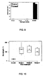
- the upper and lower ends of the lines extending from each box indicate the range of values measured for each recipe; the upper and lower ends of the boxes indicate the range bounded by the 75th and 25th centile measurements for a recipe; the horizontal line within each box indicates the median value; and the dot (where indicated) shows the mean value of the measurements for a recipe.
- Fig. 10 shows die strength measurements of laser drilled only and plasma isotropically etched die. All die had 3 slots. The increases in die strength was found to be true for both wafers plasma etched in a parallel plate and the barrel etch configurations.
- Fig. 10 shows the die strength measured from wafers etched according to 3 different recipes and from an un-etched wafer. The wafers were etched in the barrel etch configuration.
- the plasma recipes used are as follows: Recipe No O 2 (sccm) CF 4 (sccm) Pressure (mT) Power (W) Time(min) Etch Depth (microns) A 3 42 350 250 90 5 B 4 42 350 250 90 6.8 C 8 42 350 250 90 10
- the mean die strength (denoted by the filled circle) is significantly higher for the plasma etched die than the unetched die. While the distribution in die strength is significantly greater in the case of the etched samples, the values of the mean are similar in each case and are of the order of 100 N as opposed to 20 N for the unetched die. The standard deviation is also similar for the three etched samples with values of 47.8 N, 35.0 N and 35.9 N for die subjected to recipe A, B, and C respectively.
- Fig. 11 shows die strength of (a) die post laser drill (control) and (b) post laser drill and plasma etched, using a parallel plate configuration, according to recipe: 10 sccm O 2 , 42 sccm CF 4 , 250 W, 350 mT, 90 mins. All die had 3 slots.
- the boxplot shown in Fig. 11 shows the die strength measured from die taken from the laser drilled only control wafer and the wafer plasma etched using the parallel plate configuration (all die had 3 slots).
- the average strength of the die from the control wafer is calculated as 14.82 N.
- the average strength of the die from the plasma etched wafer is 57.23 N.
- plasma isotropic etching increases die strength significantly over the unetched slotted die.
- Fig. 11 shows the die strength for silicon die with 3 slots per die
- Fig. 12 shows the die strength of unetched and etched die which have 2 slots per die with longer length slots.
- Fig. 12 shows die strength of (a) unetched die (2 slots per die) post laser drill (control) and (b) die post laser drill and plasma etched ( 2 slots per die), using a parallel plate configuration, according to recipe: 10 sccm O 2 , 42 sccm CF 4 , 250 W, 350 mT, 90 mins.
Applications Claiming Priority (2)
| Application Number | Priority Date | Filing Date | Title |
|---|---|---|---|
| GB0401872A GB2410465A (en) | 2004-01-29 | 2004-01-29 | Method of making an inkjet printhead |
| GB0401872 | 2004-01-29 |
Publications (1)
| Publication Number | Publication Date |
|---|---|
| EP1559553A1 true EP1559553A1 (fr) | 2005-08-03 |
Family
ID=31971616
Family Applications (1)
| Application Number | Title | Priority Date | Filing Date |
|---|---|---|---|
| EP05100500A Withdrawn EP1559553A1 (fr) | 2004-01-29 | 2005-01-26 | Procédé de fabrication d'une tête d'impression par jet d'encre |
Country Status (4)
| Country | Link |
|---|---|
| US (1) | US20050185017A1 (fr) |
| EP (1) | EP1559553A1 (fr) |
| JP (1) | JP4611045B2 (fr) |
| GB (1) | GB2410465A (fr) |
Families Citing this family (2)
| Publication number | Priority date | Publication date | Assignee | Title |
|---|---|---|---|---|
| KR100570822B1 (ko) * | 2004-05-11 | 2006-04-12 | 삼성전자주식회사 | 잉크젯 헤드의 제조방법 및 그에 의해 제조된 잉크젯 헤드 |
| KR101562201B1 (ko) * | 2008-10-01 | 2015-10-22 | 삼성전자주식회사 | 잉크젯 프린터 헤드 및 그의 제조방법 |
Citations (10)
| Publication number | Priority date | Publication date | Assignee | Title |
|---|---|---|---|---|
| JPS5569142A (en) * | 1978-11-20 | 1980-05-24 | Fujitsu Ltd | Preventing method for peeling of resist |
| EP0609012A2 (fr) * | 1993-01-25 | 1994-08-03 | Hewlett-Packard Company | Méthode pour la fabrication d'une tête d'impression thermique par jet d'encre |
| JPH07333850A (ja) * | 1994-06-14 | 1995-12-22 | Sony Corp | 感光性組成物 |
| US6209993B1 (en) * | 1998-05-29 | 2001-04-03 | Industrial Technology Research Institute | Structure and fabricating method for ink-jet printhead chip |
| US20020149654A1 (en) * | 2001-02-22 | 2002-10-17 | Anagnostopoulos Constantine N. | CMOS/MEMS integrated ink jet print head with heater elements formed during CMOS processing and method of forming same |
| US20020180840A1 (en) * | 2001-03-22 | 2002-12-05 | Nobuo Matsumoto | Liquid ejection apparatus and inkjet printer, and method of manufacturing them |
| US6563079B1 (en) * | 1999-02-25 | 2003-05-13 | Seiko Epson Corporation | Method for machining work by laser beam |
| US6560871B1 (en) * | 2000-03-21 | 2003-05-13 | Hewlett-Packard Development Company, L.P. | Semiconductor substrate having increased facture strength and method of forming the same |
| EP1314563A2 (fr) * | 2001-11-27 | 2003-05-28 | Canon Kabushiki Kaisha | Tête à jet d'encre et sa méthode de fabrication |
| US20030117449A1 (en) * | 2001-12-20 | 2003-06-26 | David Cahill | Method of laser machining a fluid slot |
Family Cites Families (10)
| Publication number | Priority date | Publication date | Assignee | Title |
|---|---|---|---|---|
| GB2302842B (en) * | 1995-07-03 | 1998-12-30 | Seiko Epson Corp | A nozzle plate, ink-jet head and manufacturing method thereof |
| DE19536429A1 (de) * | 1995-09-29 | 1997-04-10 | Siemens Ag | Tintenstrahldruckkopf und Verfahren zum Herstellen eines solchen Tintenstrahldruckkopfes |
| US6171510B1 (en) * | 1997-10-30 | 2001-01-09 | Applied Materials Inc. | Method for making ink-jet printer nozzles |
| US6204182B1 (en) * | 1998-03-02 | 2001-03-20 | Hewlett-Packard Company | In-situ fluid jet orifice |
| US6663221B2 (en) * | 2000-12-06 | 2003-12-16 | Eastman Kodak Company | Page wide ink jet printing |
| KR100506082B1 (ko) * | 2000-12-18 | 2005-08-04 | 삼성전자주식회사 | 반구형 잉크 챔버를 가진 잉크 젯 프린트 헤드의 제조 방법 |
| US6409312B1 (en) * | 2001-03-27 | 2002-06-25 | Lexmark International, Inc. | Ink jet printer nozzle plate and process therefor |
| US6766817B2 (en) * | 2001-07-25 | 2004-07-27 | Tubarc Technologies, Llc | Fluid conduction utilizing a reversible unsaturated siphon with tubarc porosity action |
| EP1297959A1 (fr) * | 2001-09-28 | 2003-04-02 | Hewlett-Packard Company | Têtes d'impression à jet d'encre |
| KR100552664B1 (ko) * | 2002-10-12 | 2006-02-20 | 삼성전자주식회사 | 측벽에 의해 한정되는 잉크 챔버를 가진 일체형 잉크젯프린트헤드 및 그 제조방법 |
-
2004
- 2004-01-29 GB GB0401872A patent/GB2410465A/en not_active Withdrawn
-
2005
- 2005-01-26 US US11/041,991 patent/US20050185017A1/en not_active Abandoned
- 2005-01-26 EP EP05100500A patent/EP1559553A1/fr not_active Withdrawn
- 2005-01-31 JP JP2005023662A patent/JP4611045B2/ja not_active Expired - Fee Related
Patent Citations (10)
| Publication number | Priority date | Publication date | Assignee | Title |
|---|---|---|---|---|
| JPS5569142A (en) * | 1978-11-20 | 1980-05-24 | Fujitsu Ltd | Preventing method for peeling of resist |
| EP0609012A2 (fr) * | 1993-01-25 | 1994-08-03 | Hewlett-Packard Company | Méthode pour la fabrication d'une tête d'impression thermique par jet d'encre |
| JPH07333850A (ja) * | 1994-06-14 | 1995-12-22 | Sony Corp | 感光性組成物 |
| US6209993B1 (en) * | 1998-05-29 | 2001-04-03 | Industrial Technology Research Institute | Structure and fabricating method for ink-jet printhead chip |
| US6563079B1 (en) * | 1999-02-25 | 2003-05-13 | Seiko Epson Corporation | Method for machining work by laser beam |
| US6560871B1 (en) * | 2000-03-21 | 2003-05-13 | Hewlett-Packard Development Company, L.P. | Semiconductor substrate having increased facture strength and method of forming the same |
| US20020149654A1 (en) * | 2001-02-22 | 2002-10-17 | Anagnostopoulos Constantine N. | CMOS/MEMS integrated ink jet print head with heater elements formed during CMOS processing and method of forming same |
| US20020180840A1 (en) * | 2001-03-22 | 2002-12-05 | Nobuo Matsumoto | Liquid ejection apparatus and inkjet printer, and method of manufacturing them |
| EP1314563A2 (fr) * | 2001-11-27 | 2003-05-28 | Canon Kabushiki Kaisha | Tête à jet d'encre et sa méthode de fabrication |
| US20030117449A1 (en) * | 2001-12-20 | 2003-06-26 | David Cahill | Method of laser machining a fluid slot |
Non-Patent Citations (2)
| Title |
|---|
| PATENT ABSTRACTS OF JAPAN vol. 004, no. 115 (P - 023) 16 August 1980 (1980-08-16) * |
| PATENT ABSTRACTS OF JAPAN vol. 1996, no. 04 30 April 1996 (1996-04-30) * |
Also Published As
| Publication number | Publication date |
|---|---|
| GB0401872D0 (en) | 2004-03-03 |
| JP4611045B2 (ja) | 2011-01-12 |
| JP2005231361A (ja) | 2005-09-02 |
| GB2410465A (en) | 2005-08-03 |
| US20050185017A1 (en) | 2005-08-25 |
Similar Documents
| Publication | Publication Date | Title |
|---|---|---|
| EP0609012B1 (fr) | Méthode pour la fabrication d'une tête d'impression thermique par jet d'encre | |
| EP0609011B1 (fr) | Méthode pour la fabrication d'une tête d'impression thermique par jet d'encre | |
| US8608288B2 (en) | Liquid drop ejector having self-aligned hole | |
| EP0764533B1 (fr) | Fabrication de fentes d'alimentation dans un substrat silicon pour une imprimante thermique à jet d'encre | |
| US6648454B1 (en) | Slotted substrate and method of making | |
| US20090135222A1 (en) | Method of making an inkjet printhead | |
| US7549224B2 (en) | Methods of making slotted substrates | |
| US8206535B2 (en) | Inkjet printheads | |
| KR100433530B1 (ko) | 일체형 잉크젯 프린트 헤드의 제조 방법 | |
| US6675476B2 (en) | Slotted substrates and techniques for forming same | |
| EP1765596B1 (fr) | Procede de modification du profil de surface d'un canal d'alimentation en encre dans une tete d' impression | |
| EP1559553A1 (fr) | Procédé de fabrication d'une tête d'impression par jet d'encre | |
| US6911155B2 (en) | Methods and systems for forming slots in a substrate | |
| JP2011011425A (ja) | 液体吐出ヘッド用ノズルプレートの製造方法 | |
| US20050196885A1 (en) | Slotted substrates and methods of forming | |
| US8980110B2 (en) | Method of manufacturing liquid ejection head and method of processing substrate | |
| KR100425331B1 (ko) | 잉크 젯 프린트 헤드의 제조 방법 | |
| JP2007007940A (ja) | 液滴吐出ヘッドの製造方法及び液滴吐出装置の製造方法 |
Legal Events
| Date | Code | Title | Description |
|---|---|---|---|
| PUAI | Public reference made under article 153(3) epc to a published international application that has entered the european phase |
Free format text: ORIGINAL CODE: 0009012 |
|
| AK | Designated contracting states |
Kind code of ref document: A1 Designated state(s): AT BE BG CH CY CZ DE DK EE ES FI FR GB GR HU IE IS IT LI LT LU MC NL PL PT RO SE SI SK TR |
|
| AX | Request for extension of the european patent |
Extension state: AL BA HR LV MK YU |
|
| RIN1 | Information on inventor provided before grant (corrected) |
Inventor name: HARVEY, ELIZABETH Inventor name: RYAN, LIAM Inventor name: DOOLEY, KEVIN Inventor name: KEENAN, PHILIP |
|
| AKX | Designation fees paid | ||
| REG | Reference to a national code |
Ref country code: DE Ref legal event code: 8566 |
|
| RBV | Designated contracting states (corrected) |
Designated state(s): DE FR GB |
|
| 17P | Request for examination filed |
Effective date: 20060127 |
|
| 17Q | First examination report despatched |
Effective date: 20071116 |
|
| STAA | Information on the status of an ep patent application or granted ep patent |
Free format text: STATUS: THE APPLICATION HAS BEEN WITHDRAWN |
|
| 18W | Application withdrawn |
Effective date: 20100813 |