Technical Field
The present invention relates to an SOI wafer,
more particularly, to an SOI wafer having
extremely high electrical reliability even in the
case that a thin silicon active layer is formed,
and to a method for producing such an SOI wafer.
Background Art
Conventionally, as a substrate for a device,
an SOI wafer wherein a silicon active layer (an
SOI layer) is formed on a support substrate has
been widely utilized. As a method for producing
such an SOI wafer, for example, it is known that a
bonding method in which two silicon wafers are
bonded together via an oxide film. In ion
implantation delamination method which is one of
bonding methods, an oxide film (an insulator
layer) is formed on a surface of a silicon wafer
(a bond wafer) to be a silicon active layer or a
base wafer to be a support substrate, and an ion-implanted
layer is formed inside the bond wafer by
implanting ions such as hydrogen from one side
surface of the bond wafer. Further, after this
bond wafer is bonded to the base wafer via the
oxide film, delamination is performed at the ion-implanted
layer by heat treatment. Thereby, an
SOI wafer in which a thin silicon active layer is
formed on the base wafer via the oxide film can be
obtained.
Further, there are also some cases that an
insulator support substrate is used and a bond
wafer is bonded to this directly, i.e., without an
oxide film.
In the case of producing an SOI wafer as
described above, a silicon wafer on the surface of
which micro pit defects with 50 nm or more in size
exist has been generally used as a bond wafer.
However, in recent years, the demand for thinning
the silicon active layer increases, and the demand
for quality of a silicon wafer applicable to this
has also become strict.
In order to reduce defects in the silicon
active layer, there has been proposed the use of
an epitaxial layer or a silicon single crystal in
so-called a neutral region (N region) where there
exist no defects caused during growth of the
single crystal which is called grown-in defects
such as FPD, LSTD and COP.
For example, there has been proposed a method
for producing an SOI wafer by forming an epitaxial
layer on a silicon wafer (a bond wafer),
implanting boron ions into the epitaxial layer,
subsequently bonding the wafer to a support
substrate via an oxide film, and further grinding
and polishing the back surface of the bond wafer
(for example, see Japanese Patent Laid-open
(Kokai) No. 10-79498 (on pages 4 - 6, in Fig.2)).
However, in the case of using the wafer on
which the epitaxial layer is formed as the bond
wafer as described above, defects in the SOI layer
can be improved, but there has been a problem that
the production cost remarkably increases because
the process for growing the epitaxial layer
increases.
On the other hand, as a bond wafer, in the
case of using a silicon wafer grown in N region
where no micro defect such as FPD and COP exists,
although it is required to accurately control
growth conditions of a silicon single crystal,
there is an advantage that process for forming the
epitaxial layer is not needed.
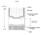
N region will be explained herein. It is
known that in the case of changing a growth rate V
from high speed to low speed in the direction of a
crystal growth axis in a CZ pulling apparatus with
a usual furnace structure (hot zone: HZ) having a
large temperature gradient G at the vicinity of a
solid-liquid interface in a crystal, a defect
distribution diagram as shown in Fig. 9 can be
obtained.
In Fig. 9, V region is a region that contains
a large amount of vacancies, i.e., depressions,
pits, or the like caused by lack of silicon atoms,
and I region is a region that contains a large
amount of dislocations or clusters of excess
silicon atoms caused by existence of excess
silicon atoms. It has also been confirmed that
there exists a neutral (hereinafter occasionally
abbreviated as N) region that contains no (or
little) lack or excess of the atom between V
region and I region, and defects called OSF
(Oxidation Induced Stacking Fault) are distributed
in a ring shape (hereinafter occasionally referred
to as OSF ring) near a boundary of V region when
observed in the cross section perpendicular to a
crystal growth axis.
When the growth rate is relatively high,
there exist grown-in defects such as FPD, LSTD and
COP, which are considered due to voids consisting
of agglomerated vacancy-type point defects, at a
high density over the entire radial direction of
the crystal, and a region containing these defects
becomes V region. Further, along with lowering of
the growth rate, the OSF ring is generated from
the periphery of the crystal. There exist at a low
density outside the OSF ring, L/D (Large
Dislocation: an abbreviation for interstitial
dislocation loop, such as LSEPD, LFPD and the
like) defects (huge dislocation clusters) which
are considered due to dislocation loops consisting
of agglomerated interstitial silicon atoms, and
the region where these defects exist becomes I
region (occasionally referred to as L/D region).
When the growth rate is further lowered, the OSF
ring shrinks to the center of the wafer and
disappears, so that the entire plane becomes I
region.
N region located between the V region and the
I region and outside the OSF ring becomes a region
containing no FPD, LSTD and COP to be generated
due to voids as well as no LSEPD and LFPD to be
generated due to interstitial silicon atoms. In
addition, it has been recently found that by
further classifying N region, as shown in Fig. 9,
there exist Nv region (the region where a lot of
vacancies exist) adjacent to the outside of OSF
ring and Ni region (the region where a lot of
interstitial silicon atoms exist) adjacent to I
region, and that when performing thermal oxidation
treatment, a lot of oxygen precipitates are
generated in Nv region and little oxygen
precipitates are generated in Ni region.
Although such an N region conventionally
existed only in a part of a plane of wafer, a
crystal having N region over the entire radial
plane (the entire surface of wafer) has been able
to be manufactured by controlling V/G that is a
ratio of a pulling rate (V) to an axial
temperature gradient (G) at a solid-liquid
interface.
Also, in the manufacture of an SOI wafer, as
described above, there has been proposed a method
in which a silicon single crystal wafer having N
region over the entire surface is used as a bond
wafer.
For example, there has been proposed an SOI
wafer wherein a silicon single crystal is pulled
by controlling a ratio of the pulling rate V to
the axial temperature gradient G at a solid-liquid
interface of the crystal (V/G) within a
predetermined range when it is pulled by
Czochralski method (CZ method), and the silicon
wafer in N region is used as a bond wafer (for
example, see Japanese Patent Laid-open (Kokai) No.
2001-146498 (on pages 5 - 8) and Japanese Patent
Laid-open (Kokai) No. 2001-44398 (on pages 2 -4,
in Fig. 1)).
However, when performing oxidation treatment
for bonding the bond wafer and the base wafer
together and oxidation treatment for adjusting the
thickness of an SOI layer, and subsequently
cleaning with hydrofluoric acid to remove an oxide
film, even if the silicon single·crystal grown in
N region is used as the bond wafer, there has been
the case that a failure such that the SOI layer
was almost entirely or partially destroyed could
occurred. Especially, the failure as described
above often occurs when a thinner SOI layer is
formed. Also, in case that making an SOI layer
thinner is further required in future, it is
apprehended that the SOI layer may be remarkably
degraded even if the silicon wafer grown simply in
N region as above is used as a bond wafer and in
addition, it is also expected that the quality of
the insulator oxide film between the SOI layer and
the base wafer may be deteriorated.
Disclosure of the Invention
The present invention was accomplished in
view of the aforementioned circumstances, and its
object is to provide an SOI wafer that has an
excellent electric property without generation of
micro pits by cleaning with hydrofluoric acid etc.
even in the case of forming an extremely thin SOI
layer with, for example, a thickness of 200nm or
less, and can be produced without increasing the
number of process.
In order to achieve the aforementioned object,
according to the present invention, there is
provided an SOI wafer in which at least a silicon
active layer is formed on a support substrate,
wherein at least the silicon active layer consists
of silicon single crystal grown by Chochralski
method, which is occupied by N region outside OSF
generated in a shape of a ring and has no defect
region detected by Cu deposition method.
As described above, in the case of the SOI
wafer of which the silicon active layer consists
of silicon single crystal being in N region and
having no defect region detected by Cu deposition
method, there does not exist even an extremely
fine defect in the silicon active layer. And
therefore, no micro pits are generated even when
it is cleaned with hydrofluoric acid etc. and it
becomes the SOI wafer having an excellent electric
property. Further, since such an SOI wafer can be
produced without increasing process as in the case
of using an epi-wafer, production cost can be
lowered.
In this case, a thickness of the silicon
active layer can be 200 nm or less.
Recently, although the SOI layer is required
to be thinner, since there does not exist even an
extremely fine defect to be detected by Cu
deposition method in the silicon active layer of
the SOI wafer according to the present invention,
even if a thickness of the silicon active layer is
200 nm or less, it is prevented that the silicon
active layer is destroyed due to enlargement of
defects by cleaning with hydrofluoric acid and the
like, so that there can be obtained an SOI wafer
with high quality.
Also, it is preferable that the silicon
active layer is formed by being bonded to the
support substrate via an oxide film, and in this
case it is preferable that a thickness of the
oxide film is in the range from 2nm to 3000nm.
If it is the SOI wafer, of which the silicon
active layer is formed by being bonded to the
support substrate via an oxide film as described
above, it can be easily produced by a general
bonding method. Further, the oxide film having a
thickness in the above-mentioned range can be
easily formed by heat treatment etc. and in
addition, the silicon active layer is surely
bonded and insulated via the oxide film so that
the SOI wafer with high quality can be obtained.
Also, the SOI wafer can be produced by ion
implantation delamination method.
As described above, if the SOI wafer is
produced by ion implantation delamination method,
the silicon active layer can be made to be
extremely thin and to have a uniform thickness and
in addition, the SOI wafer with extremely high
quality having no defect can be obtained.
Moreover, in the present invention, there is
also provided a method for producing an SOI wafer
as follows. Namely, there is provided a method
for producing an SOI wafer comprising steps of, in
a bond wafer that is to be a silicon active layer
and a base wafer that is to be a support substrate,
implanting hydrogen ions, rare gas ions or mixture
gas ions of these gases from a surface of the bond
wafer to form an ion-implanted layer inside the
bond wafer, bonding the surface of the ion-implanted
side of the bond wafer and a surface of
the base wafer via an oxide film or directly, and
subsequently delaminating a part of the bond wafer
at the ion-implanted layer by heat treatment to
form an SOI wafer, wherein a silicon wafer
consisting of silicon single crystal grown by
Chochralski method, which is occupied by N region
outside OSF generated in a shape of a ring and has
no defect region detected by Cu deposition method,
is used as the bond wafer.
If an SOI wafer is produced by such a method,
the silicon active layer reflects the
characteristic of the bond wafer, i.e., it is
occupied by N region and does not have even a
defect region to be detected by Cu deposition
method, and therefore, the SOI wafer with
extremely high quality can be obtained. Further,
since the number of processes does not increase,
production cost can be lowered.
As explained above, according to the present
invention, there is provided an SOI wafer having
an excellent electric property wherein the silicon
active layer is in a neutral (N) region without
containing V region, OSF region and huge
dislocation cluster (LSEP, LFPD) region, further
does not contain Cu deposition defect region
either, and no micro pits are generated on the
surface during manufacturing process of the SOI
wafer.
If a device is fabricated by using such an
SOI wafer, a device having an excellent electric
property can be fabricated with high yield.
Brief Explanation of the Drawings
Fig. 1 is a flowchart showing an example of a
manufacturing process of an SOI wafer according to
the present invention.
Fig. 2 shows an explanatory view showing a
region of a crystal used for manufacturing an SOI
wafer according to the present invention.
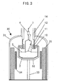
Fig. 3 shows an example of an apparatus for
producing a CZ silicon single crystal that can be
used in the present invention.
Fig. 4 (A) shows the relationship between a
growth rate of a single crystal and a cutting
position of the crystal, and Fig. 4 (B) is an
explanatory view showing the relationship between
a growth rate and each region.
Fig. 5 is an explanatory view showing a
method for producing a sample for Cu deposition
evaluation.
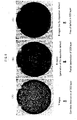
Fig. 6 shows (A) wafer lifetime and (B) Cu
deposition defects in a cross-section when cutting
a crystal lengthwise.
Fig. 7 shows the relationship between a
growth rate and a cutting position of a crystal in
Experiment 2.
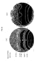
Fig. 8 shows a defect distribution of each
region of a crystal by Cu deposition method:
(A) V region, (B) N region (generation of Cu deposition
defects), (C) N region (no Cu deposition defect).
Fig. 9 is an explanatory view showing a
region of a crystal conventionally used as a bond
wafer.
Best Mode for Carrying out the Invention
Hereinafter, the present invention will be
explained in more detail.
The inventors of the present invention
performed the following investigations and studies
before accomplishment of the present invention.
First, it has been known that, in the case of
gradually lowering a growth rate from high speed
to low speed from a shoulder to an tail of
straight body of a crystal when pulling the
silicon single crystal, OSF shrinks at a certain
growth rate, and after that, phases of, in order,
Nv region, Ni region and I (huge dislocation
clusters generating) region are formed in lower
speed regions. Recently, it has been also found
that there partially exists in Nv region, a region
where defects can be detected by Cu deposition
method immediately after disappearance of OSF, as
shown in Fig. 2 (for example, see Japanese Patent
Laid-open (Kokai) 2002-201093).
Cu deposition method is a method for
evaluating a wafer by which positions of defects
in a semiconductor wafer can be accurately
measured, detection limit for defects in the
semiconductor wafer can be improved, and finer
defects can be accurately measured and analyzed.
The specific evaluation method of a wafer
comprises forming an insulator film with a
predetermined thickness on a surface of the wafer,
destroying the insulator film on the defect part
formed near the surface of the wafer, and
depositing electrolyte such as Cu at the defect
part. Namely, Cu deposition method is an
evaluation method utilizing the fact that when
electric potential is applied to an oxide film
formed on the surface of the wafer in the liquid
where Cu ions are dissolved, electric current
flows to the part where the oxide film is degraded,
and Cu ions are precipitated as Cu. It is known
that defects such as COPs exist in the part where
an oxide film is apt to be degraded.
The defect part of the wafer where Cu is
deposited can be analyzed by observation with the
naked eye under a collimated light or directly, to
evaluate a distribution and density thereof.
Furthermore, it can also be confirmed by
microscope observation, a transmission electron
microscope (TEM), a scanning electron microscope
(SEM), or the like.
And those skilled in the art could easily
conceive the use of a silicon single crystal grown
in the range from Nv region after OSF shrinks to a
position where Ni region disappears (to a position
where I region occurs) as a bond wafer (see Fig.
9).
However, as to an extremely thin SOI layer
having a thickness of, for example, 200 nm or less,
it is preferable that even a micro pit defect does
not remain therein. Then, the inventors of the
present invention investigated defects in these
regions. Specifically, when a growth rate of a
silicon single crystal is gradually lowered from
high speed to low speed, the V region just before
disappearance of OSF was subjected to FIB (focused
ion beam) processing after identification of a
coordinate by a surface inspection apparatus
(MAGICS). When the points were observed by TEM,
the existence of micro pit defects with about 20
nm could be confirmed.
Further investigations and studies as to the
other regions were performed, and the followings
were found.
Voids become finer as V region is a region
just before disappearance of OSF, however, micro
pit defects in V region remarkably deteriorate an
time zero dielectric breakdown (TZDB)
characteristic even if they are considerably fine.
On the other hand, when gradually lowering a
growth rate of a silicon single crystal from high
speed to low speed, as to Cu deposition defect
region immediately after disappearance of OSF,
there is no marked deterioration of breakdown
voltage level as in V region, and although the
TZDB characteristic indicates C mode in a region
of almost 100% in plane, a little deterioration in
time dependent dielectric breakdown (TDDB)
characteristic can be seen.
Further, it was found that existence of micro
pit defects on a surface of an SOI layer causes
breaking of the SOI layer by enlargement of the
defect size because of etching when cleaning with
hydrofluoric acid performed after oxidation for
bonding the bond wafer and the base wafer and
oxidation treatment for adjusting a thickness of
the SOI layer. In particular, in the case that an
SOI layer is thinned to have a thickness of less
than 100 nm for the purpose of expanding a
depletion layer, even if the defects are fine
enough to have a size of below 20 nm, which can be
detected by Cu deposition method, when these
defects exist, the defect size may be enlarged by
etching to thereby destroy the SOI layer when
cleaning with hydrofluoric acid. As a result,
these fine defects cause electrical fault and
remarkable derogation of reliability.
Namely, it was found that the oxide
dielectric breakdown voltage in the aforementioned
regions, especially N region, is not inherently so
low, however, when the silicon single crystal are
used as an active layer of an SOI wafer, even if
the size of defects is fine enough in comparison
with a thickness of the SOI layer, there is a
possibility of derogation of electrical
reliability.
As a result of the aforementioned
investigations and studies as above, the inventors
of the present invention found that if the silicon
active layer is occupied by N region and does not
have even a defect region detected by Cu
deposition method, there can be obtained an SOI
wafer which has an excellent electrical property,
wherein it excels in TZDB characteristic and TDDB
characteristic, and in addition which dose not
cause enlargement of the defect size and
destruction by etching even when it is subjected
to cleaning with hydrofluoric acid. And the
inventors of the present invention found that, in
order to manufacture such an SOI wafer, an SOI
layer may be formed using as a bond wafer, for
example, a silicon wafer which consists of silicon
single crystal grown by CZ method, occupied by N
region and having no defect region detected by Cu
deposition method. Thus, they accomplished the
present invention.
Hereinafter, embodiments of the present
invention will be explained in detail by referring
to the appended drawings, but the present
invention is not limited thereto.
Fig. 1 is a flowchart showing an example of a
manufacturing process of an SOI wafer according to
the present invention by ion implantation
delamination method.
First, in the first process (a), two mirror-polished
silicon wafers, i.e., a bond wafer 21
that is to be SOI layer and a base wafer 22 that
is to be a substrate, are prepared. Here in the
present invention, a silicon wafer consisting of a
silicon single crystal grown by Czochralski method
(CZ method), which is occupied by N region outside
OSF generated in a ring shape and has no defect
region detected by Cu deposition method (in the
present invention, occasionally referred to as "Cu
deposition defect region"), is used as the bond
wafer 21.
The aforementioned silicon single crystal
which has N region and no Cu deposition defect
region can be grown while controlling V/G by using,
for example, an apparatus for producing a single
crystal as shown in Fig. 3. The apparatus 30 for
pulling a single crystal has a pulling chamber 31,
a crucible 32 installed in the pulling chamber 31,
a heater 34 disposed around the crucible 32, a
crucible holding shaft 33 and a rotation mechanism
(not shown) thereof for rotating the crucible 32,
a seed chuck 6 for holding a silicon seed crystal,
a wire 7 for pulling the seed chuck 6, and a
winding mechanism (not shown) for rotating or
winding up the wire 7. A heat insulation material
35 is disposed around heater 34.
The crucible 32 is composed of an inner
quartz crucible for accommodating a silicon melt
(melt) 2 and an outer graphite crucible located
outside the quartz crucible.
Recently, it is also often the case that a
method, so-called MCZ method, is used in which
magnets not shown are disposed horizontally
outside the pulling chamber 31 and a magnetic
field in the horizontal direction, the vertical
direction, or the like is applied to the silicon
melt 2 to inhabit convection of the melt and
achieve stable growth of a single crystal.
A cylindrical graphite cylinder (heat
shielding plate) 12 is provided as surrounding a
grown silicon single crystal 1, and further in the
vicinity of a solid-liquid interface 4 of the
crystal, an annular outer heat insulation material
10 and an inner heat insulation material 11 are
provided outside and inside the cylinder,
respectively. These heat insulation materials 10
and 11 are disposed so that a gap of 2 - 20 cm is
formed between each lower end and a surface 3 of
the silicon melt 2. Thereby, difference between
temperature gradient Gc [°C/cm] at the center part
of the crystal and temperature gradient Ge in the
periphery of the crystal becomes small, and it is
also possible to control temperature inside a
furnace so that, for example, the temperature
gradient in the periphery of the crystal is lower
than that at the center of the crystal.
A cooling cylinder 14 is placed on the
graphite cylinder 12 to perform forced cooling by
flowing refrigerant inside. Furthermore, it is
also possible to provide a cylindrical cooling
device that cools a single crystal by blowing
cooling gas or shielding radiant heat.
In order to produce a silicon single crystal
using the apparatus 30 for pulling a single
crystal, first, a highly pure polycrystalline
material of silicon is heated to the melting point
(approximately 1420 °C) or higher to be melted in
the crucible 32. Then, the tip end of the seed
crystal is brought into contact with or immersed
in the approximately central portion of the
surface of the melt 2 by unwinding the wire 7.
Subsequently, while the crucible holding shaft 33
is rotated, the wire 7 is wound up with being
rotated. Thereby, the seed crystal is also pulled
with rotating, and growth of a silicon single
crystal is initiated. Then, an approximately
cylindrical single crystal ingot 1 can be obtained
by adequate control of a pulling rate and
temperature.
In order to grow a silicon single crystal
having N region and no Cu deposition defect region,
for example, a crystal is grown with controlling a
growth rate between the growth rate at the
boundary where the defect region detected by Cu
deposition method remaining after disappearance of
OSF ring is disappeared when gradually decreasing
a growth rate of silicon single crystal during
pulling and the growth rate at the boundary where
interstitial dislocation loop is generated when
gradually decreasing a growth rate of silicon
single crystal further. Namely, when a growth
rate of a silicon single crystal being pulling is
gradually lowered from high speed to low speed
from the shoulder of the crystal through the tail
of straight body thereof, as shown in Fig. 2, each
phase of, in order, V region, OSF ring region, Cu
deposition defect region, Nv region, Ni region and
I region (huge dislocation cluster generating
region) is formed depending on its growth rate.
And, the single crystal is grown by controlling a
growth rate between the growth rate at the
boundary where a defect region detected by Cu
deposition method remaining after disappearance of
OSF ring disappears in N region and the growth
rate at which I region is generated when the
growth rate is gradually lowered further. By this
manner, a silicon single crystal of N region
containing neither of V region defects such as FPD,
I region defects such as huge dislocation clusters
(LSEPD, LFPD), OSF defects, nor defects detected
by Cu deposition method can be grown.
After the silicon single crystal grown as
described above is fabricated into mirror-polished
wafer (PW), the PW is picked out at random from a
unit lot for each ingot block and then evaluation
by Cu deposition is performed. Thus, in the case
of free of defects, the wafer can be applied as a
bond wafer.
Next, in the process (b) of Fig. 1, a surface
of at least either of the bond wafer 21 or the
base wafer 22 is oxidized. The bond wafer 21 can
be thermally oxidized herein to form an oxide film
23, for example, having a thickness of 2 nm - 3000
nm on its surface. If a thickness of the oxide
film 23 is less than 2 nm, there is a possibility
that an insulation property cannot be retained.
On the other hand, if the oxide film 23 having a
thickness over 3000 nm is formed, there may occur
a problem of decrease of productivity such that
heat treatment time becomes extremely long or the
like. Therefore, it is preferable that the
thickness is within the range described above.
In the process (c), hydrogen ions are
implanted from one surface of the bond wafer 21 on
the surface of which the oxide film 23 is formed.
Rare gas ions or mixture gas ions of hydrogen ions
and rare gas ions may also be implanted. Thereby,
an ion-implanted layer parallel to the surface of
the wafer at an average penetration depth of ions
can be formed inside the wafer. The depth of the
ion-implanted layer is reflected in a thickness of
an SOI layer to be formed finally. Accordingly,
by implanting ions with controlling implantation
energy etc., it is also possible to make an SOI
layer having a thickness of for example 200 nm or
less.
In the process (d), the surface of the ion-implanted
side of the bond wafer 21 and a surface
of the base wafer 22 are bonded together via the
oxide film 23. For example, by contacting
surfaces of two wafers 21 and 22 with each other
under a clean atmosphere at room temperature, both
wafers are bonded without an adhesive agent, or
the like.
Next, in the process (e), a part of the bond
wafer 21 is delaminated at the ion-implanted layer
24 by heat treatment. For example, if the wafers
in which the bond wafer 21 and the base wafer 22
are bonded together are subjected to a heat
treatment under an inert gas atmosphere at a
temperature of about 500 °C or more, the wafers
are separated into a delaminated wafer 25 and an
SOI wafer 26 (an SOI layer 27 + a buried oxide
film 23 + the base wafer 22) due to rearrangement
of the crystal and aggregation of bubbles.
In the process (f), the SOI wafer 26 is
subjected to a bonding heat treatment. In this
process (f), since bonding strength between the
wafers brought into close contact in the
aforementioned bonding step (d) and the
delamination heat treatment step (e) is too weak
to be used as it is in a device fabrication
process, the SOI wafer 26 is subjected to a heat
treatment at high temperature as a bonding heat
treatment to be sufficient bonding strength. For
example, this heat treatment can be performed in a
range from 30 minutes to 2 hours at 1050 °C -
1200°C under an inert gas atmosphere.
In the process (g), an oxide film formed on
the surface of the SOI wafer 26 is removed by
cleaning with hydrofluoric acid. At this time, in
the case of using as a bond wafer a silicon wafer
grown simply in N region according to a
conventional way, micro pits may be generated.
However, since the SOI wafer 26 according to the
present invention is that the SOI layer 27 is
occupied by N region and has no Cu deposition
defect region, neither the pits enlarge by
cleaning with hydrofluoric acid, nor the SOI layer
27 is destroyed.
Further, in the process (h), according to
need, oxidation for adjusting a thickness of the
SOI layer 27 is performed and subsequently in the
process (I), an oxide film 28 is removed by
cleaning with hydrofluoric acid. Thereby, a
thickness of the SOI layer can be adjusted to, for
example, 200 nm or less.
The SOI wafer manufactured through the
processes (a) - (I) as described above has no
micro pit on a surface of the SOI wafer and its
electrical property becomes extremely excellent.
Hereinafter, the present invention will be
explained in reference to an example, however, the
present invention is not limited thereto.
(Examples)
(Experiment 1): Confirmation of pulling conditions
By using the apparatus 30 for producing a
single crystal shown in Fig.3, the experiment on
gradual lowering of a crystal growth rate was
performed as described below and the growth rates
at boundaries between respective regions were
examined.
First, 150 kg of polycrystalline silicon as a
raw material was charged in a quartz crucible
having a diameter of 24 inches (600 mm), and a
silicon single crystal having a diameter of 210 mm
was grown. Oxygen concentration was controlled in
the range of 23 - 26 ppma (ASTM' 79 value). When
pulling the single crystal, as shown in Fig. 4 (A),
a growth rate was controlled to be linearly and
gradually lowered from a head to a tail of the
crystal in the range from 0.70 mm/min to 0.30
mm/min.
Then, as shown in Figs. 4 (A) and (B), the
pulled single crystal was cut lengthwise in the
direction of the crystal growth axis from the head
to the tail of the pulled single crystal, and
after that, mirror-polished samples in a shape of
a wafer having a diameter of 200 mm were produced.
As to one of the samples, a distribution of
each region of V region, OSF region and I region,
and the growth rates at the boundaries of the
regions were confirmed by means of wafer lifetime
(WLT) measurement (measuring instrument: SEMILAB
WT-85) after heat treatment for oxygen
precipitation. Further, another sample was
subjected to Cu deposition treatment after forming
a thermal oxide film, and a distribution of oxide
film defects was confirmed. The detailed
evaluation process in this experiment will be
given below.
Results
The results as shown in Figs. 6 (A) and (B)
were obtained from the above-mentioned experiment,
and growth rates at the boundaries of regions such
as V region, OSF region, N region and I region
were confirmed.
(Experiment 2): Manufacture of an SOI wafer
In the same apparatus as Experiment 1 shown
in Fig. 3, 150kg of polycrystalline silicon as a
raw material was charged into a 24-inch quartz
crucible. In this time, as shown in Fig. 7, a
growth rate was lowered more gradually than that
in Experiment 1 in the range from 0.55 mm/min to
0.45 mm/min from a head to a tail of an ingot with
a diameter of 210 mm, and controlled so that N
region including Cu deposition defects and N
region without including Cu deposition defects
were formed in the region from 40 cm to 70 cm of a
straight body of a crystal. Also, the crystal was
produced so that the oxygen concentration was 24 -
26 ppma (ASTM'79). Then, the quality evaluation
and SOI processing were performed according to the
following procedure.
After that, SOI wafers having an SOI layer with a
thickness of 50 nm were produced.
When the surfaces of the SOI layer of these
SOI wafers were measured with a particle counter
(Surfscan SP-1, product of KLA-Tencor Cooperation),
it was found that SOI layers wherein silicon
wafers having V region or OSF region were used as
bond wafers were almost completely destroyed (Fig.
8 (A)).
Also, as to the bond wafer in N region where
Cu deposition defects was generated, the SOI layer
was partially destroyed in low density (Fig. 8
(B)) .
However, in the case of using the bond wafer
in N region without Cu deposition defects, no
defect could be observed on the SOI layer (Fig. 8
(C)). Further, no etch pit defect could be found
on the SOI layer in N region without Cu deposition
defect even in the case of performing measurement
of defect density after leaving the SOI wafers in
hydrofluoric acid solution of 50 % for 30 minutes
without stirring.
The present invention is not limited to the
embodiment described above. The above-described
embodiment is mere an example, and those having
substantially the same structure as technical
ideas described in the appended claims and
providing the similar functions and advantages are
included in the scope of the present invention.
For example, in the embodiment, the case of
producing an SOI wafer by using two silicon wafers
by ion implantation delamination method was
explained, but the present invention is not
limited to this production method. For example,
the present invention can also be applied to the
case of producing an SOI wafer by directly bonding
a silicon wafer as a bond wafer, which consists of
silicon single crystal grown by Czochralski method,
occupied by N region outside OSF generated in a
ring shape, and having no defect region detected
by Cu deposition method, to an insulator support
substrate such as quartz, SiC and sapphire without
an oxide film.
Furthermore, in also the case of using SIMOX
method, namely, a method for producing an SOI
wafer by heat treatment after implanting oxygen
ions into a silicon wafer, an SOI wafer according
to the present invention can be produced by using
a silicon wafer consisting of silicon single
crystal grown by Czochralski method, which is
occupied by N region outside OSF generated in a
ring shape and has no defect region detected by Cu
deposition method.