EP1553637A2 - Photovoltaic device - Google Patents
Photovoltaic device Download PDFInfo
- Publication number
- EP1553637A2 EP1553637A2 EP05100040A EP05100040A EP1553637A2 EP 1553637 A2 EP1553637 A2 EP 1553637A2 EP 05100040 A EP05100040 A EP 05100040A EP 05100040 A EP05100040 A EP 05100040A EP 1553637 A2 EP1553637 A2 EP 1553637A2
- Authority
- EP
- European Patent Office
- Prior art keywords
- transparent electrode
- structured
- photovoltaic device
- electrode
- transparent
- Prior art date
- Legal status (The legal status is an assumption and is not a legal conclusion. Google has not performed a legal analysis and makes no representation as to the accuracy of the status listed.)
- Withdrawn
Links
- 239000000758 substrate Substances 0.000 claims abstract description 95
- 229910021424 microcrystalline silicon Inorganic materials 0.000 claims abstract description 93
- XUIMIQQOPSSXEZ-UHFFFAOYSA-N Silicon Chemical compound [Si] XUIMIQQOPSSXEZ-UHFFFAOYSA-N 0.000 claims abstract description 84
- 229910052710 silicon Inorganic materials 0.000 claims abstract description 84
- 239000010703 silicon Substances 0.000 claims abstract description 84
- 239000010410 layer Substances 0.000 claims description 353
- 229910021417 amorphous silicon Inorganic materials 0.000 claims description 60
- 239000011529 conductive interlayer Substances 0.000 claims description 23
- 230000003595 spectral effect Effects 0.000 claims description 21
- 230000035945 sensitivity Effects 0.000 claims description 20
- LEVVHYCKPQWKOP-UHFFFAOYSA-N [Si].[Ge] Chemical compound [Si].[Ge] LEVVHYCKPQWKOP-UHFFFAOYSA-N 0.000 claims description 12
- 238000000151 deposition Methods 0.000 abstract description 16
- XLOMVQKBTHCTTD-UHFFFAOYSA-N Zinc monoxide Chemical compound [Zn]=O XLOMVQKBTHCTTD-UHFFFAOYSA-N 0.000 description 159
- 238000006243 chemical reaction Methods 0.000 description 133
- 239000011787 zinc oxide Substances 0.000 description 74
- 238000002834 transmittance Methods 0.000 description 51
- 239000007789 gas Substances 0.000 description 45
- 238000004544 sputter deposition Methods 0.000 description 43
- 230000007423 decrease Effects 0.000 description 39
- 239000011701 zinc Substances 0.000 description 38
- 230000003247 decreasing effect Effects 0.000 description 29
- 239000010408 film Substances 0.000 description 26
- 239000002994 raw material Substances 0.000 description 25
- QVGXLLKOCUKJST-UHFFFAOYSA-N atomic oxygen Chemical compound [O] QVGXLLKOCUKJST-UHFFFAOYSA-N 0.000 description 20
- 239000001301 oxygen Substances 0.000 description 20
- 229910052760 oxygen Inorganic materials 0.000 description 20
- BLRPTPMANUNPDV-UHFFFAOYSA-N Silane Chemical compound [SiH4] BLRPTPMANUNPDV-UHFFFAOYSA-N 0.000 description 18
- 230000008021 deposition Effects 0.000 description 15
- 238000000623 plasma-assisted chemical vapour deposition Methods 0.000 description 14
- XKRFYHLGVUSROY-UHFFFAOYSA-N Argon Chemical compound [Ar] XKRFYHLGVUSROY-UHFFFAOYSA-N 0.000 description 12
- 239000002019 doping agent Substances 0.000 description 12
- 229910052733 gallium Inorganic materials 0.000 description 12
- 230000001105 regulatory effect Effects 0.000 description 12
- GYHNNYVSQQEPJS-UHFFFAOYSA-N Gallium Chemical compound [Ga] GYHNNYVSQQEPJS-UHFFFAOYSA-N 0.000 description 10
- 230000005611 electricity Effects 0.000 description 9
- XOLBLPGZBRYERU-UHFFFAOYSA-N tin dioxide Chemical compound O=[Sn]=O XOLBLPGZBRYERU-UHFFFAOYSA-N 0.000 description 9
- 238000000034 method Methods 0.000 description 8
- 230000000052 comparative effect Effects 0.000 description 7
- 238000011835 investigation Methods 0.000 description 7
- 229910052786 argon Inorganic materials 0.000 description 6
- 239000012300 argon atmosphere Substances 0.000 description 6
- 239000012298 atmosphere Substances 0.000 description 6
- 230000000694 effects Effects 0.000 description 6
- 238000004519 manufacturing process Methods 0.000 description 6
- UFHFLCQGNIYNRP-UHFFFAOYSA-N Hydrogen Chemical compound [H][H] UFHFLCQGNIYNRP-UHFFFAOYSA-N 0.000 description 4
- 238000010790 dilution Methods 0.000 description 4
- 239000012895 dilution Substances 0.000 description 4
- 239000001257 hydrogen Substances 0.000 description 4
- 229910052739 hydrogen Inorganic materials 0.000 description 4
- 239000011229 interlayer Substances 0.000 description 4
- 229910000077 silane Inorganic materials 0.000 description 4
- XLYOFNOQVPJJNP-UHFFFAOYSA-N water Chemical compound O XLYOFNOQVPJJNP-UHFFFAOYSA-N 0.000 description 4
- 241001354532 Holozonia filipes Species 0.000 description 3
- 229910052782 aluminium Inorganic materials 0.000 description 3
- 239000005331 crown glasses (windows) Substances 0.000 description 3
- 229910001887 tin oxide Inorganic materials 0.000 description 3
- KRHYYFGTRYWZRS-UHFFFAOYSA-N Fluorane Chemical compound F KRHYYFGTRYWZRS-UHFFFAOYSA-N 0.000 description 2
- 229910021627 Tin(IV) chloride Inorganic materials 0.000 description 2
- QUZPNFFHZPRKJD-UHFFFAOYSA-N germane Chemical compound [GeH4] QUZPNFFHZPRKJD-UHFFFAOYSA-N 0.000 description 2
- 229910052986 germanium hydride Inorganic materials 0.000 description 2
- 239000005361 soda-lime glass Substances 0.000 description 2
- 229910001220 stainless steel Inorganic materials 0.000 description 2
- 239000010935 stainless steel Substances 0.000 description 2
- 239000010409 thin film Substances 0.000 description 2
- HPGGPRDJHPYFRM-UHFFFAOYSA-J tin(iv) chloride Chemical compound Cl[Sn](Cl)(Cl)Cl HPGGPRDJHPYFRM-UHFFFAOYSA-J 0.000 description 2
- PXGOKWXKJXAPGV-UHFFFAOYSA-N Fluorine Chemical compound FF PXGOKWXKJXAPGV-UHFFFAOYSA-N 0.000 description 1
- 206010021143 Hypoxia Diseases 0.000 description 1
- XAGFODPZIPBFFR-UHFFFAOYSA-N aluminium Chemical compound [Al] XAGFODPZIPBFFR-UHFFFAOYSA-N 0.000 description 1
- 238000005516 engineering process Methods 0.000 description 1
- 229910052731 fluorine Inorganic materials 0.000 description 1
- 239000011737 fluorine Substances 0.000 description 1
- 230000001678 irradiating effect Effects 0.000 description 1
- 239000000463 material Substances 0.000 description 1
- 229910052751 metal Inorganic materials 0.000 description 1
- 239000002184 metal Substances 0.000 description 1
- 238000010248 power generation Methods 0.000 description 1
- 239000004065 semiconductor Substances 0.000 description 1
- 229910052709 silver Inorganic materials 0.000 description 1
- 238000007738 vacuum evaporation Methods 0.000 description 1
Images

Classifications
-
- H—ELECTRICITY
- H01—ELECTRIC ELEMENTS
- H01L—SEMICONDUCTOR DEVICES NOT COVERED BY CLASS H10
- H01L31/00—Semiconductor devices sensitive to infrared radiation, light, electromagnetic radiation of shorter wavelength or corpuscular radiation and specially adapted either for the conversion of the energy of such radiation into electrical energy or for the control of electrical energy by such radiation; Processes or apparatus specially adapted for the manufacture or treatment thereof or of parts thereof; Details thereof
- H01L31/18—Processes or apparatus specially adapted for the manufacture or treatment of these devices or of parts thereof
- H01L31/1884—Manufacture of transparent electrodes, e.g. TCO, ITO
-
- H—ELECTRICITY
- H01—ELECTRIC ELEMENTS
- H01L—SEMICONDUCTOR DEVICES NOT COVERED BY CLASS H10
- H01L31/00—Semiconductor devices sensitive to infrared radiation, light, electromagnetic radiation of shorter wavelength or corpuscular radiation and specially adapted either for the conversion of the energy of such radiation into electrical energy or for the control of electrical energy by such radiation; Processes or apparatus specially adapted for the manufacture or treatment thereof or of parts thereof; Details thereof
- H01L31/02—Details
- H01L31/0224—Electrodes
- H01L31/022466—Electrodes made of transparent conductive layers, e.g. TCO, ITO layers
- H01L31/022483—Electrodes made of transparent conductive layers, e.g. TCO, ITO layers composed of zinc oxide [ZnO]
-
- H—ELECTRICITY
- H01—ELECTRIC ELEMENTS
- H01L—SEMICONDUCTOR DEVICES NOT COVERED BY CLASS H10
- H01L31/00—Semiconductor devices sensitive to infrared radiation, light, electromagnetic radiation of shorter wavelength or corpuscular radiation and specially adapted either for the conversion of the energy of such radiation into electrical energy or for the control of electrical energy by such radiation; Processes or apparatus specially adapted for the manufacture or treatment thereof or of parts thereof; Details thereof
- H01L31/04—Semiconductor devices sensitive to infrared radiation, light, electromagnetic radiation of shorter wavelength or corpuscular radiation and specially adapted either for the conversion of the energy of such radiation into electrical energy or for the control of electrical energy by such radiation; Processes or apparatus specially adapted for the manufacture or treatment thereof or of parts thereof; Details thereof adapted as photovoltaic [PV] conversion devices
- H01L31/06—Semiconductor devices sensitive to infrared radiation, light, electromagnetic radiation of shorter wavelength or corpuscular radiation and specially adapted either for the conversion of the energy of such radiation into electrical energy or for the control of electrical energy by such radiation; Processes or apparatus specially adapted for the manufacture or treatment thereof or of parts thereof; Details thereof adapted as photovoltaic [PV] conversion devices characterised by at least one potential-jump barrier or surface barrier
- H01L31/075—Semiconductor devices sensitive to infrared radiation, light, electromagnetic radiation of shorter wavelength or corpuscular radiation and specially adapted either for the conversion of the energy of such radiation into electrical energy or for the control of electrical energy by such radiation; Processes or apparatus specially adapted for the manufacture or treatment thereof or of parts thereof; Details thereof adapted as photovoltaic [PV] conversion devices characterised by at least one potential-jump barrier or surface barrier the potential barriers being only of the PIN type
- H01L31/076—Multiple junction or tandem solar cells
-
- Y—GENERAL TAGGING OF NEW TECHNOLOGICAL DEVELOPMENTS; GENERAL TAGGING OF CROSS-SECTIONAL TECHNOLOGIES SPANNING OVER SEVERAL SECTIONS OF THE IPC; TECHNICAL SUBJECTS COVERED BY FORMER USPC CROSS-REFERENCE ART COLLECTIONS [XRACs] AND DIGESTS
- Y02—TECHNOLOGIES OR APPLICATIONS FOR MITIGATION OR ADAPTATION AGAINST CLIMATE CHANGE
- Y02E—REDUCTION OF GREENHOUSE GAS [GHG] EMISSIONS, RELATED TO ENERGY GENERATION, TRANSMISSION OR DISTRIBUTION
- Y02E10/00—Energy generation through renewable energy sources
- Y02E10/50—Photovoltaic [PV] energy
- Y02E10/547—Monocrystalline silicon PV cells
-
- Y—GENERAL TAGGING OF NEW TECHNOLOGICAL DEVELOPMENTS; GENERAL TAGGING OF CROSS-SECTIONAL TECHNOLOGIES SPANNING OVER SEVERAL SECTIONS OF THE IPC; TECHNICAL SUBJECTS COVERED BY FORMER USPC CROSS-REFERENCE ART COLLECTIONS [XRACs] AND DIGESTS
- Y02—TECHNOLOGIES OR APPLICATIONS FOR MITIGATION OR ADAPTATION AGAINST CLIMATE CHANGE
- Y02E—REDUCTION OF GREENHOUSE GAS [GHG] EMISSIONS, RELATED TO ENERGY GENERATION, TRANSMISSION OR DISTRIBUTION
- Y02E10/00—Energy generation through renewable energy sources
- Y02E10/50—Photovoltaic [PV] energy
- Y02E10/548—Amorphous silicon PV cells
Definitions
- the present invention relates to photovoltaic devices having transparent electrodes made of zinc oxide (ZnO).
- photovoltaic devices include silicon-based thin-film photovoltaic devices, such as solar cells. These photovoltaic devices in general include a substrate having thereon a first transparent electrode, silicon-based semiconductor layers (photovoltaic layers), a second transparent electrode, and a metal electrode film, laminated from bottom to top in that order.
- These transparent electrodes must be made of materials with low resistance and high light transmittance, such as zinc oxide (ZnO) and tin oxide (SnO 2 ).
- a low-resistance transparent electrode can be realized by adding, for example, gallium (Ga) oxide, aluminum (Al) oxide, or fluorine.
- a technology in which a transparent electrode film is formed at low temperatures by adding Ga to a ZnO layer in a case where photovoltaic layers are made of amorphous silicon thin films is also known, as disclosed in Japanese Unexamined Patent Application Publication (Kokai) No. Hei 6-338623 (see paragraphs [0006] and [0014] and Fig. 1 therein).
- Ga oxide or Al oxide to produce a low-resistance transparent electrode, however, results in a decrease in transmittance of the transparent electrode.
- addition of Ga or Al to an oxide-based transparent conductive layer causes both the resistivity and transmittance to decrease. In other words, it is difficult to achieve desired aspects of both resistivity and transmittance by adding Al or Ga.
- Hei 6-338623 does not examine the Ga concentration to increase the photovoltaic conversion efficiency by focusing on how the addition of Ga affects the interface between the Si layer (p layer or n layer) and the ZnO:Ga layer or the resistivity and the transmittance of the ZnO:Ga layer. Thus, there is still room for improvement of the photovoltaic conversion efficiency in photovoltaic devices.
- the present invention was conceived in light of the above circumstances, and it is an object of the present invention to provide a photovoltaic device that realizes a high photovoltaic conversion efficiency by the use of a transparent electrode or a transparent conductive layer having an optimal relationship between the resistivity and transmittance, within a range where the quality of the interface between the Si layer (p layer or n layer) and the ZnO:Ga layer is not degraded by the addition of Ga.
- a photovoltaic device adopts the following features.
- a photovoltaic device includes an electrically insulating transparent substrate; a first transparent electrode; PIN-structured or NIP-structured microcrystalline silicon layers including a p-type silicon layer, an i-type silicon layer, and an n-type silicon layer; a second transparent electrode; and a back electrode.
- the first transparent electrode, the PIN-structured or NIP-structured microcrystalline silicon layers, the second transparent electrode, and the back electrode are deposited in sequence on the electrically insulating transparent substrate.
- At least one of the first transparent electrode and the second transparent electrode is a ZnO layer doped with Ga, and the Ga concentration is 15 atomic percent or less with respect to Zn.
- This photovoltaic device receives light via the electrically insulating transparent substrate.
- Adding gallium (Ga) oxide to the zinc oxide (ZnO) layer functioning as a transparent electrode causes the conductivity to increase and the transmittance to decrease.
- the inventors of the present invention as a result of through investigation, have found that the photovoltaic conversion efficiency can be maintained up to a certain level (e.g., several ⁇ cm) of resistivity in order to satisfy the performance requirements of the photovoltaic device. Therefore, decreasing the Ga concentration to the upper resistivity limit at which the conversion efficiency is maintained is expected to cause the conversion efficiency to increase due to an increase in the transmittance resulting from the decrease in the Ga concentration.
- a similar effect can also be achieved by adding oxygen to the atmosphere during sputtering instead of decreasing the Ga concentration.
- the process according to the present invention has an advantage in that a decrease in the amount of Ga leads to an increase in the quality of the interface between the Si layer (p layer or n layer) and the ZnO:Ga layer.
- a Ga concentration of 15 atomic percent or less with respect to Zn causes the photovoltaic conversion efficiency to increase for a single photovoltaic device including microcrystalline silicon layers according to the present invention.
- the Ga-doped ZnO layer according to the present invention be employed for the second transparent electrode adjacent to the back electrode because the ZnO layer increases reflectance.
- the phrase "15 atomic percent or less" according to the present invention includes 0 atomic percent if it causes the efficiency to increase.
- the Ga concentration preferably ranges from 0.02 to 10 atomic percent, and more preferably from 0.5 to 2 atomic percent.
- a photovoltaic device includes an electrically insulating substrate; a back electrode; a first transparent electrode; PIN-structured or NIP-structured microcrystalline silicon layers including a p-type silicon layer, an i-type silicon layer, and an n-type silicon layer; a second transparent electrode; and a collecting electrode.
- the back electrode, the first transparent electrode, the PIN-structured or NIP-structured microcrystalline silicon layers, the second transparent electrode, and the collecting electrode are deposited in sequence on the electrically insulating substrate.
- At least one of the first transparent electrode and the second transparent electrode is a ZnO layer doped with Ga, and the Ga concentration is 15 atomic percent or less with respect to Zn.
- This photovoltaic device receives light via the collecting electrode.
- Adding gallium (Ga) to the zinc oxide (ZnO) layer functioning as a transparent electrode causes the conductivity to increase and the transmittance to decrease.
- the inventors of the present invention as a result of through investigation, have found that the photovoltaic conversion efficiency can be maintained up to a certain level (e.g., several ⁇ cm) of resistivity in order to satisfy the performance requirements of the photovoltaic device. Therefore, decreasing the Ga concentration to the upper resistivity limit at which the conversion efficiency is maintained is expected to cause the conversion efficiency to increase due to an increase in the transmittance resulting from the decrease in the Ga concentration.
- a similar effect can also be achieved by adding oxygen to the atmosphere during sputtering instead of decreasing the Ga concentration.
- the process according to the present invention has an advantage in that a decrease in the amount of Ga leads to an increase in the quality of the interface between the Si layer and the ZnO:Ga layer.
- a Ga concentration of 15 atomic percent or less with respect to Zn causes the photovoltaic conversion efficiency to increase for a single photovoltaic device including microcrystalline silicon layers according to the present invention.
- the Ga-doped ZnO layer according to the present invention be employed for the first transparent electrode adjacent to the electrically insulating substrate because the ZnO layer increases reflectance.
- the phrase "15 atomic percent or less" according to the present invention includes 0 atomic percent if it causes the efficiency to increase.
- the Ga concentration preferably ranges from 0.02 to 10 atomic percent, and more preferably from 0.5 to 2 atomic percent.
- a photovoltaic device includes an electrically insulating transparent substrate; a first transparent electrode; PIN-structured or NIP-structured amorphous silicon layers including a p-type silicon layer, an i-type silicon layer, and an n-type silicon layer; a second transparent electrode; and a back electrode.
- the first transparent electrode, the PIN-structured or NIP-structured amorphous silicon layers, the second transparent electrode, and the back electrode are deposited in sequence on the electrically insulating transparent substrate.
- At least one of the first transparent electrode and the second transparent electrode is a ZnO layer doped with Ga, and the Ga concentration is 2 atomic percent or less with respect to Zn.
- This photovoltaic device receives light via the electrically insulating transparent substrate.
- Adding gallium (Ga) oxide to the zinc oxide (ZnO) layer functioning as a transparent electrode causes the conductivity to increase and the transmittance to decrease.
- the inventors of the present invention as a result of through investigation, have found that the photovoltaic conversion efficiency can be maintained up to a certain level (e.g., several ⁇ cm) of resistivity in order to satisfy the performance requirements of the photovoltaic device. Therefore, decreasing the Ga concentration to the upper resistivity limit at which the conversion efficiency is maintained is expected to cause the conversion efficiency to increase due to an increase in the transmittance resulting from the decrease in the Ga concentration.
- a similar effect can also be achieved by adding oxygen to the atmosphere during sputtering instead of decreasing the Ga concentration.
- the process according to the present invention has an advantage in that a decrease in the amount of Ga leads to an increase in the quality of the interface between the Si layer and the ZnO:Ga layer.
- a Ga concentration of 2 atomic percent or less with respect to Zn causes the photovoltaic conversion efficiency to increase for a single photovoltaic device including amorphous silicon layers according to the present invention.
- the Ga-doped ZnO layer according to the present invention be employed for the second transparent electrode adjacent to the back electrode because the ZnO layer increases reflectance.
- the phrase "2 atomic percent or less" according to the present invention includes 0 atomic percent if it causes the efficiency to increase.
- the Ga concentration preferably ranges from 0.02 to 1.7 atomic percent, and more preferably from 0.7 to 1.3 atomic percent.
- a photovoltaic device includes an electrically insulating substrate; a back electrode; a first transparent electrode; PIN-structured or NIP-structured amorphous silicon layers including a p-type silicon layer, an i-type silicon layer, and an n-type silicon layer; a second transparent electrode; and a collecting electrode.
- the back electrode, the first transparent electrode, the PIN-structured or NIP-structured amorphous silicon layers, the second transparent electrode, and the collecting electrode are deposited in sequence on the electrically insulating substrate.
- At least one of the first transparent electrode and the second transparent electrode is a ZnO layer doped with Ga, and the Ga concentration is 2 atomic percent or less with respect to Zn.
- This photovoltaic device receives light via the collecting electrode.
- Adding gallium (Ga) oxide to the zinc oxide (ZnO) layer functioning as a transparent electrode causes the conductivity to increase and the transmittance to decrease.
- the inventors of the present invention as a result of through investigation, have found that the photovoltaic conversion efficiency can be maintained up to a certain level (e.g., several ⁇ cm) of resistivity in order to satisfy the performance requirements of the photovoltaic device. Therefore, decreasing the Ga concentration to the upper resistivity limit at which the conversion efficiency is maintained is expected to cause the conversion efficiency to increase due to an increase in the transmittance resulting from the decrease in the Ga concentration.
- a similar effect can also be achieved by adding oxygen to the atmosphere during sputtering instead of decreasing the Ga concentration.
- the process according to the present invention has an advantage in that a decrease in the amount of Ga leads to an increase in the quality of the interface between the Si layer and the ZnO:Ga layer.
- a Ga concentration of 2 atomic percent or less with respect to Zn causes the photovoltaic conversion efficiency to increase for a single photovoltaic device including amorphous silicon layers according to the present invention.
- the Ga-doped ZnO layer according to the present invention be employed for the first transparent electrode adjacent to the electrically insulating substrate because the ZnO layer increases reflectance.
- the phrase "2 atomic percent or less" according to the present invention includes 0 atomic percent if it causes the efficiency to increase.
- the Ga concentration preferably ranges from 0.02 to 1.7 atomic percent, and more preferably from 0.7 to 1.3 atomic percent.
- the photovoltaic device according to the present invention may further include PIN-structured or NIP-structured amorphous silicon layers disposed between the first transparent electrode or the second transparent electrode and the PIN-structured or NIP-structured microcrystalline silicon layers.
- the photovoltaic device with the above-described structure is a tandem photovoltaic device including microcrystalline silicon layers and amorphous silicon layers.
- the tandem photovoltaic device adding gallium (Ga) to the zinc oxide (ZnO) layer functioning as a transparent electrode causes the conductivity to increase and the transmittance to decrease.
- Ga gallium
- ZnO zinc oxide
- the inventors of the present invention as a result of through investigation, have found that the photovoltaic conversion efficiency can be maintained up to a certain level (e.g., several ⁇ cm) of resistivity in order to satisfy the performance requirements of the photovoltaic device. Therefore, decreasing the Ga concentration to the upper resistivity limit at which the conversion efficiency is maintained is expected to cause the conversion efficiency to increase due to an increase in the transmittance resulting from the decrease in the Ga concentration.
- a similar effect can also be achieved by adding oxygen to the atmosphere during sputtering instead of decreasing the Ga concentration.
- the process according to the present invention has an advantage in that a decrease in the amount of Ga leads to an increase in the quality of the interface between the Si layer and the ZnO:Ga layer.
- a Ga concentration of 15 atomic percent or less with respect to Zn causes the photovoltaic conversion efficiency to increase for a tandem photovoltaic device according to the present invention.
- the Ga-doped ZnO layer according to the present invention be employed for the second transparent electrode adjacent to the back electrode or the first transparent electrode adjacent to the electrically insulating substrate because the ZnO layer increases reflectance.
- the phrase "15 atomic percent or less" according to the present invention includes 0 atomic percent if it causes the efficiency to increase.
- the Ga concentration preferably ranges from 0.02 to 10 atomic percent, and more preferably from 0.5 to 2 atomic percent.
- the photovoltaic device according to the present invention may further include a transparent conductive interlayer disposed between the amorphous silicon layers and the microcrystalline silicon layers.
- the transparent conductive interlayer is a ZnO layer doped with Ga, and the Ga concentration is 15 atomic percent or less with respect to Zn.
- the transparent conductive interlayer is disposed between the microcrystalline silicon layers and the amorphous silicon layers as an interlayer, where the Ga concentration is 15 atomic percent or less. This increases the efficiency as described above.
- the phrase "15 atomic percent or less" according to the present invention includes 0 atomic percent if it causes the efficiency to increase.
- the Ga concentration preferably ranges from 0.02 to 10 atomic percent, and more preferably from 0.5 to 2 atomic percent.
- the photovoltaic device according to the present invention may further include other PIN-structured or NIP-structured microcrystalline silicon layers having a different spectral sensitivity or microcrystalline silicon germanium layers having a different spectral sensitivity disposed between the first transparent electrode or the second transparent electrode and the PIN-structured or NIP-structured microcrystalline silicon layers.
- the photovoltaic device with the above-described structure is a tandem photovoltaic device including microcrystalline silicon layers and microcrystalline silicon layers with different spectral sensitivity or microcrystalline silicon germanium layers with different spectral sensitivity.
- the tandem photovoltaic device adding gallium (Ga) to the zinc oxide (ZnO) layer functioning as a transparent electrode causes the conductivity to increase and the transmittance to decrease.
- Ga gallium
- ZnO zinc oxide
- the inventors of the present invention as a result of through investigation, have found that the photovoltaic conversion efficiency can be maintained up to a certain level (e.g., several ⁇ cm) of resistivity in order to satisfy the performance requirements of the photovoltaic device. Therefore, decreasing the Ga concentration to the upper resistivity limit at which the conversion efficiency is maintained is expected to cause the conversion efficiency to increase due to an increase in the transmittance resulting from the decrease in the Ga concentration.
- a similar effect can also be achieved by adding oxygen to the atmosphere during sputtering instead of decreasing the Ga concentration.
- the process according to the present invention has an advantage in that a decrease in the amount of Ga leads to an increase in the quality of the interface between the Si layer and the ZnO:Ga layer.
- a Ga concentration of 15 atomic percent or less with respect to Zn causes the photovoltaic conversion efficiency to increase for a tandem photovoltaic device according to the present invention.
- the Ga-doped ZnO layer according to the present invention be employed for the second transparent electrode adjacent to the back electrode or the first transparent electrode adjacent to the electrically insulating substrate because the ZnO layer increases reflectance.
- the phrase "15 atomic percent or less" according to the present invention includes 0 atomic percent if it causes the efficiency to increase.
- the Ga concentration preferably ranges from 0.02 to 10 atomic percent, and more preferably from 0.5 to 2 atomic percent.
- the photovoltaic device may further include a transparent conductive interlayer disposed between the microcrystalline silicon layers and the other PIN-structured or NIP-structured microcrystalline silicon layers having a different spectral sensitivity or the microcrystalline silicon germanium layers having a different spectral sensitivity.
- the transparent conductive interlayer is a ZnO layer doped with Ga, and the Ga concentration is 15 atomic percent or less with respect to Zn.
- the transparent conductive interlayer as an interlayer is disposed between the microcrystalline silicon layers and microcrystalline silicon layers with spectral sensitivity or microcrystalline silicon germanium layers with spectral sensitivity, where the Ga concentration is 15 atomic percent or less. This increases the efficiency as described above.
- the phrase "15 atomic percent or less" according to the present invention includes 0 atomic percent if it causes the efficiency to increase.
- the Ga concentration preferably ranges from 0.02 to 10 atomic percent, and more preferably from 0.5 to 2 atomic percent.
- a Ga-doped ZnO layer is used for the transparent electrodes or the transparent conductive layer, where the Ga concentration is a certain level or less with respect to Zn. More specifically, the Ga concentration is decreased to its minimum possible level, i.e., the upper resistivity limit of the transparent electrodes or the transparent conductive layer at which the desired photovoltaic conversion efficiency is maintained. Because of this, the transmittance can be prevented from being decreased, and consequently, a transparent electrode with high transmittance over a wide range of wavelengths can be produced. Thus, it is no longer necessary to add oxygen during the deposition of the ZnO layers to enhance the transmittance. This decreases the damage to the transparent electrodes by oxygen, and therefore, the controllability and yield during film deposition are enhanced.
- the photovoltaic layers can receive more intense light to increase the short-circuit current density.
- the photovoltaic conversion efficiency thus increases.
- a decrease in the Ga concentration enhances the quality of the interface between the p-type and n-type silicon layers for high open-circuit voltage, short-circuit current density, and fill factor. This also leads to an increase in the photovoltaic conversion efficiency.
- a photovoltaic device according to a first embodiment of the present invention is described with reference to Fig. 1.
- the photovoltaic device includes electricity-generating layers made of microcrystalline silicon and receives incident light via an electrically insulating transparent substrate.
- a first transparent electrode 12 is formed on an electrically insulating transparent substrate 11.
- Optically transparent white crown glass for example, can be used for the electrically insulating transparent substrate 11.
- the first transparent electrode 12 is made of zinc oxide (ZnO) doped with gallium (Ga). Furthermore, an antireduction film may be formed on the first transparent electrode 12.
- the electrically insulating transparent substrate 11 is housed in a DC sputtering apparatus, and a Ga-doped ZnO layer is formed on the transparent electrically insulating substrate 11 by evacuating the reaction chamber to a vacuum, filling the reaction chamber with a predetermined volume of argon gas, and then performing DC sputtering in this argon atmosphere.
- the Ga concentration is 15 atomic percent or less with respect to Zn, preferably 0.02 to 10 atomic percent, and more preferably 0.5 to 2 atomic percent.
- the pressure in the DC sputtering apparatus is preferably about 0.6 Pa
- the temperature of the electrically insulating transparent substrate 11 is preferably 80°C to 135°C
- the sputtering power is preferably about 100 W.
- the conductivity increases, whereas the transmittance decreases.
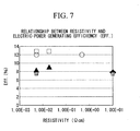
- the inventors of the present invention as a result of through investigation, have found that a drastic decrease in the resistivity is not required to increase the photovoltaic conversion efficiency; that is, the photovoltaic conversion efficiency can be increased while maintaining a certain level (e.g., several ⁇ cm) of resistivity in order to satisfy the performance requirements of the photovoltaic device.
- Fig. 7 shows the relationship between the resistivity of a transparent electrode (horizontal axis) and the conversion efficiency of a photovoltaic device (vertical axis).
- the plots in Fig. 7 represent the results for cells manufactured under the same conditions except for the Ga concentration (cells that can be compared on the basis of absolute values).
- the conversion efficiency does not decrease despite the resistivity being increased to about 10 ⁇ cm. Therefore, decreasing the Ga concentration to the upper resistivity limit at which the conversion efficiency is maintained is expected to cause the conversion efficiency to increase due to an increase in the transmittance.
- a decrease in the amount of Ga leads to an increase in the quality of the interface between the Si layer and the ZnO:Ga layer.
- the processing object is housed in a reaction chamber, which is then evacuated to a vacuum using a vacuum pump. Then, the electricity supply to a heater incorporated in the anode is turned on, and the substrate, i.e., the processing object, is heated, for example, to 160°C or higher. SiH 4 , H 2 , and p-type dopant gas, which are raw material gases, are then introduced into the reaction chamber, and the pressure in the reaction chamber is regulated at a predetermined level.
- very-high-frequency electrical power is supplied from a very-high-frequency electrical power supply to a discharge electrode to generate a plasma between the discharge electrode and the processing object, and thereby a p-type microcrystalline silicon layer 13 is formed on the first transparent electrode 12 of the processing object.
- B 2 H 6 or the like may be used as the p-type dopant gas.
- the electrically insulating transparent substrate 11 is housed again in a reaction chamber of another plasma enhanced CVD apparatus, and the interior of the reaction chamber is evacuated to a vacuum.
- a mixed gas of SiH 4 and H 2 which are raw material gases, is then introduced into the reaction chamber, and the pressure in the reaction chamber is regulated at a predetermined level.
- very-high-frequency electrical power with a frequency of 60 MHz or higher is supplied from a very-high-frequency electrical power supply to a discharge electrode to generate a plasma between the discharge electrode and the processing object, and thereby an i-type microcrystalline silicon layer 14 is formed on the p-type silicon layer 13 of the processing object.
- the pressure in the interior of the reaction chamber for generating plasma in the reaction chamber is preferably in the range of 0.5 to 10 Torr, and more preferably in the range of 1.0 to 6.0 Torr.
- the electrically insulating transparent substrate 11 is housed as a processing object in another reaction chamber which is evacuated to a vacuum.
- SiH 4 , H 2 , and n-type dopant gas (such as PH 3 ), which are raw material gases, are introduced into this reaction chamber, and the pressure in the reaction chamber is regulated at a predetermined level.
- very-high-frequency electrical power is supplied from a very-high-frequency electrical power supply to a discharge electrode to generate a plasma between the discharge electrode and the processing object, and thereby an n-type microcrystalline silicon layer 15 is formed on the i-type silicon layer 14.
- the processing object is then taken out of the plasma enhanced CVD apparatus.
- the electrically insulating transparent substrate 11 having layers up to the n-type silicon layer 15 formed thereon is housed in the DC sputtering apparatus.
- a Ga-doped ZnO layer is formed as a second transparent electrode 16 on the n-type silicon layer 15.
- the Ga-doped ZnO layer is formed on the n-type silicon layer 15 by evacuating the reaction chamber to a vacuum, filling the reaction chamber with a predetermined volume of argon gas, and then performing DC sputtering in this argon atmosphere.
- the Ga concentration is 15 atomic percent or less with respect to Zn, preferably 0.02 to 10 atomic percent, and more preferably 0.5 to 2 atomic percent.
- the pressure in the DC sputtering apparatus is preferably about 0.6 Pa
- the temperature of the electrically insulating transparent substrate 11 is preferably 80°C to 135°C
- the sputtering power is preferably about 100 W.
- an Ag film or Al film is formed as a back electrode 17 on the second transparent electrode 16 by, for example, sputtering or vacuum evaporation deposition.
- the photovoltaic device manufactured as described above generates electricity by photovoltaic conversion from incident light, such as sunlight, entering the microcrystalline silicon layers 13, 14, and 15 with the above-described PIN structure via the electrically insulating transparent substrate 11.
- a PIN structure is constructed by forming the p-type silicon layer 13, the i-type silicon layer 14, and the n-type silicon layer 15 in sequence from the first transparent electrode 12 side; however, an NIP structure may also be constructed by forming n-type, i-type, and p-type silicon layers in sequence.
- ZnO layers having a Ga concentration of 15 atomic percent or less with respect to Zn are used for both the first transparent electrode 12 and the second transparent electrode 16 in the first embodiment, the present invention is not limited to this structure. Such a ZnO layer may be used for either the first transparent electrode 12 or the second transparent electrode 16.
- a Ga-doped ZnO layer according to the present invention be employed for the second transparent electrode 16 adjacent to the back electrode 17 because a transparent electrode here increases the reflectance.
- Ga-doped ZnO layers are used for the transparent electrodes 12 and 16, where the Ga concentration is 15 atomic percent or less with respect to Zn. More specifically, the Ga concentration is decreased to its minimum possible level, i.e., the upper resistivity limit at which the desired photovoltaic conversion efficiency is maintained. Because of this, the transmittance can be prevented from being decreased, and consequently, a transparent electrode with high transmittance over a wide range of wavelengths can be produced. Thus, it is no longer necessary to add oxygen during the deposition of the ZnO layers to enhance the transmittance. This decreases the damage to the transparent electrodes by oxygen, and therefore, the controllability and yield during film deposition are enhanced.
- the photovoltaic layers can receive more intense light to increase the short-circuit current density.
- the photovoltaic conversion efficiency thus increases.
- a decrease in the Ga concentration enhances the quality of the interface between the p-type and n-type silicon layers for high open-circuit voltage, short-circuit current density, and fill factor. This also leads to an increase in the photovoltaic conversion efficiency.
- a photovoltaic device according to a second embodiment of the present invention is described with reference to Fig. 2.
- the photovoltaic device according to the second embodiment is similar to the photovoltaic device according to the first embodiment in that electricity-generating layers are made of microcrystalline silicon. Unlike the photovoltaic device according to the first embodiment, the photovoltaic device according to the second embodiment is constructed so as to receive incident light via an opposite collecting electrode to enable an electrically insulating opaque substrate to be used.
- a back electrode 17 and a first transparent electrode 22 are formed on an electrically insulating opaque substrate 21 that does not transmit light.
- a stainless steel plate for example, is used as the electrically insulating opaque substrate 21. Soda-lime glass may be used in place of the electrically insulating opaque substrate 21.
- Ga zinc oxide (ZnO) doped with gallium (Ga) is used for the first transparent electrode 22, where the Ga concentration is 15 atomic percent or less with respect to Zn, preferably 0.02 to 10 atomic percent, and more preferably 0.5 to 2 atomic percent.
- ZnO zinc oxide
- Ga gallium
- an antireduction film may be formed on the first transparent electrode 22.
- an n-type microcrystalline silicon layer 15, an i-type microcrystalline silicon layer 14, and a p-type microcrystalline silicon layer 13 are formed in the same manner as in the first embodiment.
- the electrically insulating opaque substrate 21 having layers up to the p-type silicon layer 13 formed thereon is housed in the DC sputtering apparatus.
- a Ga-doped ZnO layer is formed as a second transparent electrode 26 in this DC sputtering apparatus, where the Ga concentration is 15 atomic percent or less with respect to Zn, preferably 0.02 to 10 atomic percent, and more preferably 0.5 to 2 atomic percent.
- an Ag film or Al film is formed as a collecting electrode 27 on the second transparent electrode 26.
- the collecting electrode 27 is formed in a mesh or stripes so as not to block the incident light.
- the photovoltaic device manufactured as described above generates electricity by photovoltaic conversion from incident light, such as sunlight, entering the microcrystalline silicon layers 15, 14, and 13 with the above-described NIP structure via the collecting electrode 27.
- an NIP structure is constructed by forming the n-type silicon layer 15, the i-type silicon layer 14, and the p-type silicon layer 13 in sequence from the first transparent electrode 22 side; however, a PIN structure may also be constructed by forming the p-type, i-type, and n-type silicon layers in sequence.
- ZnO layers having a Ga concentration of 15 atomic percent or less with respect to Zn are used for both the first transparent electrode 22 and the second transparent electrode 26 in the second embodiment, the present invention is not limited to this structure. Such a ZnO layer may be used for either the first transparent electrode 22 or the second transparent electrode 26.
- a Ga-doped ZnO layer according to the present invention be employed for the first transparent electrode 22 adjacent to the electrically insulating opaque substrate 21 because a transparent electrode here increases the reflectance.
- Ga-doped ZnO layers are used for the transparent electrodes 22 and 26, where the Ga concentration is 15 atomic percent or less with respect to Zn. More specifically, the Ga concentration is decreased to its minimum possible level, i.e., the upper resistivity limit at which the desired photovoltaic conversion efficiency is maintained. Because of this, the transmittance can be prevented from being decreased, and consequently, a transparent electrode with high transmittance over a wide range of wavelengths can be produced. Thus, it is no longer necessary to add oxygen during the deposition of the ZnO layers to enhance the transmittance. This decreases the damage to the transparent electrodes by oxygen, and therefore, the controllability and yield during film deposition are enhanced.
- the photovoltaic layers can receive more intense light to increase the short-circuit current density.
- the photovoltaic conversion efficiency thus increases.
- a decrease in the Ga concentration enhances the quality of the interface between the p-type and n-type silicon layers for high open-circuit voltage, short-circuit current density, and fill factor. This also leads to an increase in the photovoltaic conversion efficiency.
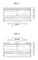
- a photovoltaic device according to a third embodiment of the present invention is described with reference to Fig. 3.
- the photovoltaic device according to the third embodiment has electricity-generating layers made of amorphous silicon.
- the photovoltaic device according to the third embodiment receives incident light via an electrically insulating transparent substrate in the same manner as with the first embodiment.
- a first transparent electrode 32 is formed on an electrically insulating transparent substrate 11.
- Optically transparent white crown glass for example, can be used for the electrically insulating transparent substrate 11.
- the first transparent electrode 32 is made of tin oxide (SnO 2 ).
- the electrically insulating transparent substrate 11 is housed in an atmospheric plasma enhanced CVD apparatus, and the first transparent electrode 32 made of SnO 2 is formed on the electrically insulating transparent substrate 11 from SnCl 4 , water vapor (H 2 O), and anhydrous hydrogen fluoride (HF) which are raw material gases.
- the processing object is housed in a reaction chamber, which is then evacuated to a vacuum using a vacuum pump. Then, the electricity supply to a heater incorporated in the anode is turned on, and the substrate, i.e., the processing object, is heated, for example, to 160°C or higher. SiH 4 , H 2 , and p-type dopant gas, which are raw material gases, are then introduced into the reaction chamber, and the pressure in the reaction chamber is regulated at a predetermined level.
- RF electrical power is supplied from an RF electrical power supply to a discharge electrode to generate a plasma between the discharge electrode and the processing object, and thereby a p-type amorphous silicon layer 33 is formed on the first transparent electrode 32 of the processing object.
- the amorphous silicon layer 33 is formed mainly by lowering the dilution ratio of silane to hydrogen compared with that according to the first embodiment. A lower dilution ratio of silane to hydrogen is also used in the third step and the fourth step.
- B 2 H 6 or the like may be used as the p-type dopant gas.
- the electrically insulating transparent substrate 11 is housed again in a reaction chamber of another plasma enhanced CVD apparatus, and the interior of the reaction chamber is evacuated to a vacuum.
- a mixed gas of SiH 4 and H 2 which are raw material gases, is then introduced into the reaction chamber, and the pressure in the reaction chamber is regulated at a predetermined level.
- very-high-frequency electrical power with a frequency of 60 MHz or higher is supplied from a very-high-frequency electrical power supply to a discharge electrode to generate a plasma between the discharge electrode and the processing object, and thereby an i-type amorphous silicon layer 34 is formed on the p-type silicon layer 33 of the processing object.
- the pressure in the interior of the reaction chamber for generating plasma in the reaction chamber is preferably in the range of 0.5 to 10 Torr, and more preferably in the range of 0.5 to 6.0 Torr.
- the i-type silicon layer 34 After the i-type silicon layer 34 is formed, introduction of the raw material gases is ceased, and the interior of the reaction chamber is evacuated to a vacuum. Then, the electrically insulating transparent substrate 11 is housed as a processing object in another reaction chamber, which is evacuated to a vacuum. SiH 4 , H 2 , and n-type dopant gas (such as PH 3 ), which are raw material gases, are introduced into this reaction chamber, and the pressure in the reaction chamber is regulated at a predetermined level.
- SiH 4 , H 2 , and n-type dopant gas such as PH 3
- very-high-frequency electrical power is supplied from a very-high-frequency electrical power supply to a discharge electrode to generate a plasma between the discharge electrode and the processing object, and thereby an n-type amorphous silicon layer 35 is formed on the i-type silicon layer 34.
- the processing object is then taken out of the plasma enhanced CVD apparatus.
- the electrically insulating transparent substrate 11 having layers up to the n-type silicon layer 35 formed thereon is housed in the DC sputtering apparatus.
- a Ga-doped ZnO layer is formed as a second transparent electrode 36 on the n-type silicon layer 35.
- the Ga-doped ZnO layer is formed on the n-type silicon layer 35 by evacuating the reaction chamber to a vacuum, filling the reaction chamber with a predetermined volume of argon gas, and then performing DC sputtering in this argon atmosphere.
- the Ga concentration is 2 atomic percent or less with respect to Zn, preferably 0.02 to 1.7 atomic percent, and more preferably 0.7 to 1.3 atomic percent.
- the pressure in the DC sputtering apparatus is preferably about 0.6 Pa
- the temperature of the electrically insulating transparent substrate 11 is preferably 80°C to 135°C
- the sputtering power is preferably about 100 W.
- the Ga concentration is determined thus for the same reason as described with reference to Fig. 7 in the first embodiment. More specifically, decreasing the Ga concentration to the upper resistivity limit at which the conversion efficiency of the photovoltaic device is maintained is expected to cause the conversion efficiency to increase due to an increase in the transmittance. Furthermore, a decrease in the amount of Ga leads to an increase in the quality of the interface between the Si layer (p-layer or n-layer) and the ZnO:Ga layer. As a result of examining the Ga concentration from this viewpoint, it has been found that a Ga concentration of 2 atomic percent or less with respect to Zn causes the photovoltaic conversion efficiency to increase for a single photovoltaic device including amorphous-silicon electricity-generating layers according to the third embodiment.
- an Ag film or Al film is formed as a back electrode 17 on the second transparent electrode 36.
- the photovoltaic device manufactured as described above generates electricity by photovoltaic conversion from incident light, such as sunlight, entering the amorphous silicon layers 33, 34, and 35 with the above-described PIN structure via the electrically insulating transparent substrate 11.
- a PIN structure is constructed by forming the p-type silicon layer 33, the i-type silicon layer 34, and the n-type silicon layer 35 in sequence from the first transparent electrode 32 side; however, an NIP structure may also be constructed by forming n-type, i-type, and p-type silicon layers in sequence.
- a ZnO layer having a Ga concentration of 2 atomic percent or less with respect to Zn is used for the second transparent electrode 36 in the third embodiment, the present invention is not limited to this structure. Such a ZnO layer may be used for the first transparent electrode 32.
- a Ga-doped ZnO layer according to the present invention be employed for the second transparent electrode 36 adjacent to the back electrode 37 because a transparent electrode here increases the reflectance.
- a Ga-doped ZnO layer is used for the second transparent electrode 36, where the Ga concentration is 2 atomic percent or less with respect to Zn. More specifically, the Ga concentration is decreased to its minimum possible level, i.e., the upper resistivity limit at which the desired photovoltaic conversion efficiency is maintained. Because of this, the transmittance can be prevented from being decreased, and consequently, a transparent electrode with high transmittance over a wide range of wavelengths can be produced. Thus, it is no longer necessary to add oxygen during the deposition of the ZnO layer to enhance the transmittance. This decreases the damage to the transparent electrode by oxygen, and therefore, the controllability and yield during film deposition are enhanced.
- the photovoltaic layers can receive more intense light to increase the short-circuit current density.
- the photovoltaic conversion efficiency thus increases.
- a decrease in the Ga concentration enhances the quality of the interface between the p-type and n-type silicon layers for high open-circuit voltage, short-circuit current density, and fill factor. This also leads to an increase in the photovoltaic conversion efficiency.
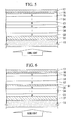
- a photovoltaic device according to a fourth embodiment of the present invention is described with reference to Fig. 4.
- the photovoltaic device according to the fourth embodiment is similar to the photovoltaic device according to the third embodiment in that electricity-generating layers are made of amorphous silicon. Unlike the photovoltaic device according to the third embodiment and just like the photovoltaic device according to the second embodiment, the photovoltaic device according to the fourth embodiment is constructed so as to receive incident light via a collecting electrode opposite to an electrically insulating opaque substrate to enable an electrically insulating opaque substrate to be used.
- a back electrode 17 and a first transparent electrode 42 are formed on an electrically insulating opaque substrate 21 that does not transmit light.
- a stainless steel plate for example, is used as the electrically insulating opaque substrate 21. Soda-lime glass may be used in place of the electrically insulating opaque substrate 21.
- the first transparent electrode 42 is made of zinc oxide (ZnO) doped with gallium (Ga).
- the electrically insulating opaque substrate 21 is housed in a DC sputtering apparatus, and a Ga-doped ZnO layer is formed on the electrically insulating opaque substrate 21 by evacuating the reaction chamber to a vacuum, filling the reaction chamber with a predetermined volume of argon gas, and then performing DC sputtering in this argon atmosphere.
- the Ga concentration is 2 atomic percent or less with respect to Zn, preferably 0.02 to 1.7 atomic percent, and more preferably 0.7 to 1.3 atomic percent. The Ga concentration is determined thus for the same reason as described in the third embodiment.
- the pressure in the DC sputtering apparatus is preferably about 0.6 Pa
- the temperature of the electrically insulating opaque substrate 21 is preferably 80°C to 135°C
- the sputtering power is preferably about 100 W.
- an n-type amorphous silicon layer 35, an i-type amorphous silicon layer 34, and a p-type amorphous silicon layer 33 are formed in the same manner as in the third embodiment.
- the electrically insulating opaque substrate 21 having layers up to the p-type silicon layer 33 formed thereon is housed in the DC sputtering apparatus.
- a SnO 2 layer is formed as a second transparent electrode 46.
- an Ag film or Al film is formed as a collecting electrode 27 on the second transparent electrode 46.
- the collecting electrode 27 is formed in a mesh or stripes so as not to block the incident light.
- the photovoltaic device manufactured as described above generates electricity by photovoltaic conversion from incident light, such as sunlight, entering the amorphous silicon layers 35, 34, and 33 with the above-described NIP structure via the collecting electrode 27.
- an NIP structure is constructed by forming the n-type silicon layer 35, the i-type silicon layer 34, and the p-type silicon layer 33 in sequence from the first transparent electrode 42 side; however, a PIN structure may also be constructed by forming the p-type, i-type, and n-type silicon layers in sequence.
- a ZnO layer having a Ga concentration of 2 atomic percent or less with respect to Zn is used for the first transparent electrode 42 in the fourth embodiment, the present invention is not limited to this structure. Such a ZnO layer may be used for the second transparent electrode 46.
- a Ga-doped ZnO layer according to the present invention be employed for the first transparent electrode 42 adjacent to the electrically insulating opaque substrate 21 because a transparent electrode here increases the reflectance.
- a Ga-doped ZnO layer is used for the transparent electrode 42, where the Ga concentration is 2 atomic percent or less with respect to Zn. More specifically, the Ga concentration is decreased to its minimum possible level, i.e., the upper resistivity limit at which the desired photovoltaic conversion efficiency is maintained. Because of this, the transmittance can be prevented from being decreased, and consequently, a transparent electrode with high transmittance over a wide range of wavelengths can be produced. Thus, it is no longer necessary to add oxygen during the deposition of the ZnO layer to enhance the transmittance. This decreases the damage to the transparent electrode by oxygen, and therefore, the controllability and yield during film deposition are enhanced.
- the photovoltaic layers can receive more intense light to increase the short-circuit current density.
- the photovoltaic conversion efficiency thus increases.
- a decrease in the Ga concentration enhances the quality of the interface between the p-type and n-type silicon layers for high open-circuit voltage, short-circuit current density, and fill factor. This also leads to an increase in the photovoltaic conversion efficiency.
- a photovoltaic device according to a fifth embodiment of the present invention is described with reference to Fig. 5.
- the photovoltaic device according to the fifth embodiment differs from those according to the first to the fourth embodiments in that the photovoltaic device according to the fifth embodiment is a tandem photovoltaic device including electricity-generating layers made of amorphous silicon and electricity-generating layers made of microcrystalline silicon.
- a first transparent electrode 32 is formed on an electrically insulating transparent substrate 11.
- Optically transparent white crown glass for example, can be used for the electrically insulating transparent substrate 11.
- the first transparent electrode 32 is made of tin oxide (SnO 2 ).
- the electrically insulating transparent substrate 11 is housed in an atmospheric plasma enhanced CVD apparatus, and the first transparent electrode 32 made of SnO 2 is formed on the electrically insulating transparent substrate 11 from SnCl 4 , water vapor (H 2 O), and anhydrous hydrogen fluoride (HF), which are raw material gases.
- the processing object is housed in a reaction chamber, which is then evacuated to a vacuum using a vacuum pump. Then, the electricity supply to a heater incorporated in the anode is turned on, and the substrate, i.e., the processing object, is heated, for example, to 160°C or higher. SiH 4 , H 2 , and p-type dopant gas, which are raw material gases, are then introduced into the reaction chamber, and the pressure in the reaction chamber is regulated at a predetermined level.
- RF electrical power is supplied from an RF electrical power supply to a discharge electrode to generate a plasma between the discharge electrode and the processing object, and thereby a p-type amorphous silicon layer 33 is formed on the first transparent electrode 32 of the processing object.
- the amorphous silicon layer 33 is formed mainly by lowering the dilution ratio of silane to hydrogen compared with that according to the first embodiment. A lower dilution ratio of silane to hydrogen is also used in the third step and the fourth step.
- B 2 H 6 or the like may be used as the p-type dopant gas.
- the electrically insulating transparent substrate 11 is housed again in a reaction chamber of another plasma enhanced CVD apparatus, and the interior of the reaction chamber is evacuated to a vacuum.
- a mixed gas of SiH 4 and H 2 which are raw material gases, is then introduced into the reaction chamber, and the pressure in the reaction chamber is regulated at a predetermined level.
- very-high-frequency electrical power with a frequency of 60 MHz or higher is supplied from a very-high-frequency electrical power supply to a discharge electrode to generate a plasma between the discharge electrode and the processing object, and thereby an i-type amorphous silicon layer 34 is formed on the p-type silicon layer 33 of the processing object.
- the pressure in the interior of the reaction chamber for generating plasma in the reaction chamber is preferably in the range of 0.5 to 10 Torr, and more preferably in the range of 0.5 to 6.0 Torr.
- the electrically insulating transparent substrate 11 is housed as a processing object in another reaction chamber which is evacuated to a vacuum.
- SiH 4 , H 2 , and n-type dopant gas (such as PH 3 ), which are raw material gases, are introduced into this reaction chamber, and the pressure in the reaction chamber is regulated at a predetermined level.
- very-high-frequency electrical power is supplied from a very-high-frequency electrical power supply to a discharge electrode to generate a plasma between the discharge electrode and the processing object, and thereby an n-type amorphous silicon layer 35 is formed on the i-type silicon layer 34.
- the processing object is then taken out of the plasma enhanced CVD apparatus.
- electricity-generating layers made of microcrystalline silicon are formed on the above-described amorphous-silicon electricity-generating layers 33, 34, and 35.
- microcrystalline silicon layers can be formed in the same manner as in the first embodiment.
- the processing object is housed in a reaction chamber, which is then evacuated to a vacuum using a vacuum pump. Then, the electricity supply to a heater incorporated in the anode is turned on, and the substrate, i.e., the processing object, is heated, for example, to 160°C or higher.
- SiH 4 , H 2 , and p-type dopant gas which are raw material gases, are then introduced into the reaction chamber, and the pressure in the reaction chamber is regulated at a predetermined level.
- very-high-frequency electrical power is supplied from a very-high-frequency electrical power supply to a discharge electrode to generate a plasma between the discharge electrode and the processing object, and thereby a p-type microcrystalline silicon layer 13 is formed on the amorphous-silicon electricity-generating layer 35 of the processing object.
- B 2 H 6 or the like may be used as the p-type dopant gas.
- the electrically insulating transparent substrate 11 is housed again in a reaction chamber of another plasma enhanced CVD apparatus, and the interior of the reaction chamber is evacuated to a vacuum.
- a mixed gas of SiH 4 and H 2 which are raw material gases, is then introduced into the reaction chamber, and the pressure in the reaction chamber is regulated at a predetermined level.
- very-high-frequency electrical power with a frequency of 60 MHz or higher is supplied from a very-high-frequency electrical power supply to a discharge electrode to generate a plasma between the discharge electrode and the processing object, and thereby an i-type microcrystalline silicon layer 14 is formed on the p-type silicon layer 13 of the processing object.
- the pressure in the interior of the reaction chamber for generating plasma in the reaction chamber is preferably in the range of 0.5 to 10 Torr, and more preferably in the range of 1.0 to 6.0 Torr.
- the i-type silicon layer 14 After the i-type silicon layer 14 is formed, introduction of the raw material gases is ceased, and the interior of the reaction chamber is evacuated to a vacuum. Then, the electrically insulating transparent substrate 11 is housed as a processing object in another reaction chamber, which is evacuated to a vacuum. SiH 4 , H 2 , and n-type dopant gas (such as PH 3 ), which are raw material gases, are introduced into this reaction chamber, and the pressure in the reaction chamber is regulated at a predetermined level.
- SiH 4 , H 2 , and n-type dopant gas such as PH 3
- very-high-frequency electrical power is supplied from a very-high-frequency electrical power supply to a discharge electrode to generate a plasma between the discharge electrode and the processing object, and thereby an n-type microcrystalline silicon layer 15 is formed on the i-type silicon layer 14.
- the processing object is then taken out of the plasma enhanced CVD apparatus.
- the electrically insulating transparent substrate 11 having layers up to the n-type silicon layer 15 formed thereon is housed in the DC sputtering apparatus.
- a Ga-doped ZnO layer is formed as a second transparent electrode 16 on the n-type silicon layer 15.
- the Ga-doped ZnO layer is formed on the n-type silicon layer 15 by evacuating the reaction chamber to a vacuum, filling the reaction chamber with a predetermined volume of argon gas, and then performing DC sputtering in this argon atmosphere.
- the Ga concentration is 15 atomic percent or less with respect to Zn, preferably 0.02 to 10 atomic percent, and more preferably 0.5 to 2 atomic percent. The Ga concentration is determined thus for the same reason as described in the first embodiment.
- the pressure in the DC sputtering apparatus is preferably about 0.6 Pa
- the temperature of the electrically insulating transparent substrate 11 is preferably 80°C to 135°C
- the sputtering power is preferably about 100 W.
- an Ag film or Al film is formed as a back electrode 17 on the second transparent electrode 16.
- the photovoltaic device manufactured as described above generates electricity by photovoltaic conversion from incident light, such as sunlight, entering the microcrystalline silicon layers 13, 14, and 15 with the above-described PIN structure via the electrically insulating transparent substrate 11.
- a PIN structure is constructed by forming the p-type amorphous silicon layer 33, the i-type amorphous silicon layer 34, and the n-type amorphous silicon layer 35 in sequence from the first transparent electrode 32 side; however, an NIP structure may also be constructed by forming the n-type, i-type, and p-type amorphous silicon layers in sequence.
- a PIN structure is constructed by forming the p-type microcrystalline silicon layer 13, the i-type microcrystalline silicon layer 14, and the n-type microcrystalline silicon layer 15 in sequence from the first transparent electrode 32 side; however, an NIP structure may also be constructed by forming the n-type, i-type, and p-type microcrystalline silicon layers in sequence.
- amorphous-silicon electricity-generating layers 33, 34, and 35 may be formed on the microcrystalline-silicon electricity-generating layers 13, 14, and 15.
- the photovoltaic device may be constructed such that the electrically insulating opaque substrate 21 is used in place of the electrically insulating transparent substrate 11 and the collecting electrode 27 is used in place of the back electrode 17 to receive incident light via the collecting electrode 27, as with the second or fourth embodiment.
- a ZnO layer having a Ga concentration of 15 atomic percent or less with respect to Zn is used for the second transparent electrode 16 in the third embodiment, the present invention is not limited to this structure. Such a ZnO layer may be used for the first transparent electrode 32.
- a Ga-doped ZnO layer according to the present invention be employed for the second transparent electrode 16 adjacent to the back electrode 17 because a transparent electrode here increases the reflectance.
- a Ga-doped ZnO layer is used for the transparent electrode 16, where the Ga concentration is 15 atomic percent or less with respect to Zn. More specifically, the Ga concentration is decreased to its minimum possible level, i.e., the upper resistivity limit at which the desired photovoltaic conversion efficiency is maintained. Because of this, the transmittance can be prevented from being decreased, and consequently, a transparent electrode with high transmittance over a wide range of wavelengths can be produced. Thus, it is no longer necessary to add oxygen during the deposition of the ZnO layer to enhance the transmittance. This decreases the damage to the transparent electrode by oxygen, and therefore, the controllability and yield during film deposition are enhanced.
- the photovoltaic layers can receive more intense light to increase the short-circuit current density.
- the photovoltaic conversion efficiency thus increases.
- a decrease in the Ga concentration enhances the quality of the interface between the p-type and n-type silicon layers for high open-circuit voltage, short-circuit current density, and fill factor. This also leads to an increase in the photovoltaic conversion efficiency.
- the tandem photovoltaic device includes electricity-generating layers made of amorphous silicon and electricity-generating layers made of microcrystalline silicon.
- the tandem photovoltaic device according to the present invention may include electricity-generating layers made of one type of microcrystalline silicon and electricity-generating layers made of another type of microcrystalline silicon with different spectral sensitivities.
- the tandem photovoltaic device according to the present invention may include electricity-generating layers made of microcrystalline silicon and electricity-generating layers made of microcrystalline silicon germanium with different spectral sensitivities.
- Microcrystalline silicon germanium can be produced from SiH 4 , GeH 4 , and H 2 serving as raw materials in the same manner as for microcrystalline silicon.
- a photovoltaic device according to a sixth embodiment of the present invention is described with reference to Fig. 6.
- the photovoltaic device according to the sixth embodiment is similar to the photovoltaic device according to the fifth embodiment in that both photovoltaic devices are tandem photovoltaic devices including electricity-generating layers made of amorphous silicon and electricity-generating layers made of microcrystalline silicon.
- the photovoltaic device according to the sixth embodiment differs from the photovoltaic device according to the fifth embodiment in that the photovoltaic device according to the sixth embodiment includes a transparent conductive interlayer between the amorphous-silicon electricity-generating layers 33 to 35 and the microcrystalline-silicon electricity-generating layers 13 to 15. The following description focuses on this difference.
- a transparent conductive interlayer 61 is formed of Ga-doped ZnO with a DC sputtering apparatus.
- a Ga-doped ZnO layer is formed as the transparent conductive interlayer 61 on the n-type amorphous silicon layer 35.
- the Ga-doped ZnO layer is formed on the n-type silicon layer 35 by evacuating the reaction chamber to a vacuum, filling the reaction chamber with a predetermined volume of argon gas, and then performing DC sputtering in this argon atmosphere.
- the Ga concentration is 15 atomic percent or less with respect to Zn, preferably 0.02 to 10 atomic percent, and more preferably 0.5 to 2 atomic percent. The Ga concentration is determined thus for the same reason as described in the first embodiment.
- the pressure in the DC sputtering apparatus is preferably about 0.6 Pa
- the temperature of the electrically insulating transparent substrate 11 is preferably from normal room temperature to 135°C
- the sputtering power is preferably about 100 W.
- the tandem photovoltaic device includes electricity-generating layers made of amorphous silicon and electricity-generating layers made of microcrystalline silicon.
- the tandem photovoltaic device according to the present invention may include electricity-generating layers made of one type of microcrystalline silicon and electricity-generating layers made of another type of microcrystalline silicon with different spectral sensitivities.
- the tandem photovoltaic device according to the present invention may include electricity-generating layers made of microcrystalline silicon and electricity-generating layers made of microcrystalline silicon germanium with different spectral sensitivities.
- Microcrystalline silicon germanium can be produced from SiH 4 , GeH 4 , and H 2 serving as raw materials in the same manner as for microcrystalline silicon.
- a photovoltaic device according to Example 1 was produced based on the first embodiment. More specifically, as shown in Fig. 1, the photovoltaic device according to Example 1 is a single photovoltaic device including microcrystalline-silicon electricity-generating layers 13, 14, and 15, where incident light enters via the electrically insulating transparent substrate 11.
- the Ga concentration was 1 atomic percent with respect to Zn.
- the film thickness of the first and second transparent electrodes 12 and 16 was 80 nm.
- the transmittance of the above-described transparent electrodes was 95% or higher in a wavelength range of 550 nm or more.
- a photovoltaic device the same as that according to Example 1, except for a Ga concentration of 9 atomic percent, was also produced.
- a photovoltaic device according to Example 2 was produced based on the third embodiment. More specifically, as shown in Fig. 3, the photovoltaic device according to Example 2 is a single photovoltaic device including amorphous-silicon electricity-generating layers 33, 34, and 35, where incident light enters via the electrically insulating transparent substrate 11.
- the Ga concentration was 1 atomic percent with respect to Zn.
- the film thickness of the second transparent electrode 36 was 80 nm.
- the transmittance of the above-described transparent electrode was 95% or higher in a wavelength range of 550 nm or more.
- a photovoltaic device the same as that according to Example 2, except for a Ga concentration of 9 atomic percent, was also produced.
- a photovoltaic device according to Example 3 was produced based on the fifth embodiment. More specifically, as shown in Fig. 5, the photovoltaic device according to Example 3 is a tandem photovoltaic device including amorphous-silicon electricity-generating layers 33, 34, and 35 and microcrystalline-silicon electricity-generating layers 13, 14, and 15, where incident light enters via the electrically insulating transparent substrate 11.
- the Ga concentration was 1 atomic percent with respect to Zn.
- the film thickness of the second transparent electrode 16 was 80 nm.
- the transmittance of the above-described transparent electrode was 95% or higher in a wavelength range of 550 nm or more.
- a photovoltaic device the same as that according to Example 3, except for a Ga concentration of 9 atomic percent, was also produced.
- a photovoltaic device according to Example 4 was produced based on the sixth embodiment. More specifically, as shown in Fig. 6, the photovoltaic device according to Example 4 is a tandem photovoltaic device including the transparent conductive interlayer 61 between the amorphous-silicon electricity-generating layers 33 to 35 and the microcrystalline-silicon electricity-generating layers 13 to 15, where incident light enters via the electrically insulating transparent substrate 11.
- the Ga concentration was 1 atomic percent with respect to Zn.
- the film thickness of the second transparent electrode 16 was 80 nm.
- the film thickness of the transparent conductive interlayer 61 was 50 nm.
- the transmittance of the above-described transparent electrode was 95% or higher in a wavelength range of 550 nm or more.
- a photovoltaic device the same as that according to Example 4, except for a Ga concentration of 9 atomic percent, was also produced.
- a decrease in the Ga concentration causes the crystallinity of the p-type silicon layers to be enhanced and the fill factor (FF) to be improved.
- the single photovoltaic device including microcrystalline silicon according to Example 1 exhibits a significant improvement in the conversion efficiency (Eff.). This is because the decrease in the amount of Ga causes the quality of the interface between the Si layer (p layer or n layer) and the ZnO:Ga layer to be improved.
Abstract
Description
Furthermore, a decrease in the amount of Ga leads to an increase in the quality of the interface between the Si layer and the ZnO:Ga layer. As a result of examining the Ga concentration from this viewpoint, it has been found that a Ga concentration of 15 atomic percent or less with respect to Zn causes the photovoltaic conversion efficiency to increase for a single photovoltaic device including microcrystalline-silicon electricity-generating layers according to the first embodiment. Second Step
| Example 1 (microcrystalline Si, single) | Example 2 (a-Si, single) | Example 3 (tandem, without interlayer) | Example 4 (tandem, with interlayer) | |||||
| comp. example | invention | comp. example | invention | comp. example | invention | comp. example | invention | |
| Ga (at.%) | 9 | 1 | 9 | 1 | 9 | 1 | 9 | 1 |
| Jsc | 1 | 1.1 | 1 | 1.05 | 1 | 1.05 | 1 | 1.08 |
| Voc | 1 | 1 | 1 | 1 | 1 | 1 | 1 | 1 |
| FF | 1 | 1 | 1 | 1 | 1 | 1.02 | 1 | 1.02 |
| Eff. | 1 | 1.08 | 1 | 1.02 | 1 | 1.03 | 1 | 1.05 |
Claims (12)
- A photovoltaic device comprising:wherein the first transparent electrode, the PIN-structured or NIP-structured microcrystalline silicon layers, the second transparent electrode, and the back electrode are deposited in sequence on the electrically insulating transparent substrate; andan electrically insulating transparent substrate;a first transparent electrode;PIN-structured or NIP-structured microcrystalline silicon layers including a p-type silicon layer, an i-type silicon layer, and an n-type silicon layer;a second transparent electrode; anda back electrode,
wherein at least one of the first transparent electrode and the second transparent electrode is a ZnO layer doped with Ga, and the Ga concentration is 15 atomic percent or less with respect to Zn. - A photovoltaic device comprising:wherein the back electrode, the first transparent electrode, the PIN-structured or NIP-structured microcrystalline silicon layers, the second transparent electrode, and the collecting electrode are deposited in sequence on the electrically insulating substrate; andan electrically insulating substrate;a back electrode;a first transparent electrode;PIN-structured or NIP-structured microcrystalline silicon layers including a p-type silicon layer, an i-type silicon layer, and an n-type silicon layer;a second transparent electrode; anda collecting electrode,
wherein at least one of the first transparent electrode and the second transparent electrode is a ZnO layer doped with Ga, and the Ga concentration is 15 atomic percent or less with respect to Zn. - A photovoltaic device comprising:wherein the first transparent electrode, the PIN-structured or NIP-structured amorphous silicon layers, the second transparent electrode, and the back electrode are deposited in sequence on the electrically insulating transparent substrate; andan electrically insulating transparent substrate;a first transparent electrode;PIN-structured or NIP-structured amorphous silicon layers including a p-type silicon layer, an i-type silicon layer, and an n-type silicon layer;a second transparent electrode; anda back electrode,
wherein at least one of the first transparent electrode and the second transparent electrode is a ZnO layer doped with Ga, and the Ga concentration is 2 atomic percent or less with respect to Zn. - A photovoltaic device comprising:wherein the back electrode, the first transparent electrode, the PIN-structured or NIP-structured amorphous silicon layers, the second transparent electrode, and the collecting electrode are deposited in sequence on the electrically insulating substrate; andan electrically insulating substrate;a back electrode;a first transparent electrode;PIN-structured or NIP-structured amorphous silicon layers including a p-type silicon layer, an i-type silicon layer, and an n-type silicon layer;a second transparent electrode; anda collecting electrode,
wherein at least one of the first transparent electrode and the second transparent electrode is a ZnO layer doped with Ga, and the Ga concentration is 2 atomic percent or less with respect to Zn. - The photovoltaic device according to claim 1, further comprising:PIN-structured or NIP-structured amorphous silicon layers disposed between the first transparent electrode or the second transparent electrode and the PIN-structured or NIP-structured microcrystalline silicon layers.
- The photovoltaic device according to claim 2, further comprising:PIN-structured or NIP-structured amorphous silicon layers disposed between the first transparent electrode or the second transparent electrode and the PIN-structured or NIP-structured microcrystalline silicon layers.
- The photovoltaic device according to claim 5, further comprising:wherein the transparent conductive interlayer is a ZnO layer doped with Ga, and the Ga concentration is 15 atomic percent or less with respect to Zn.a transparent conductive interlayer disposed between the amorphous silicon layers and the microcrystalline silicon layers,
- The photovoltaic device according to claim 6, further comprising:wherein the transparent conductive interlayer is a ZnO layer doped with Ga, and the Ga concentration is 15 atomic percent or less with respect to Zn.a transparent conductive interlayer disposed between the amorphous silicon layers and the microcrystalline silicon layers,
- The photovoltaic device according to claim 1, further comprising:other PIN-structured or NIP-structured microcrystalline silicon layers having a different spectral sensitivity or microcrystalline silicon germanium layers having a different spectral sensitivity disposed between the first transparent electrode or the second transparent electrode and the PIN-structured or NIP-structured microcrystalline silicon layers.
- The photovoltaic device according to claim 2, further comprising:other PIN-structured or NIP-structured microcrystalline silicon layers having a different spectral sensitivity or microcrystalline silicon germanium layers having a different spectral sensitivity disposed between the first transparent electrode or the second transparent electrode and the PIN-structured or NIP-structured microcrystalline silicon layers.
- The photovoltaic device according to claim 9, further comprising:wherein the transparent conductive interlayer is a ZnO layer doped with Ga, and the Ga concentration is 15 atomic percent or less with respect to Zn.a transparent conductive interlayer disposed between the microcrystalline silicon layers and the other PIN-structured or NIP-structured microcrystalline silicon layers having a different spectral sensitivity or the microcrystalline silicon germanium layers having a different spectral sensitivity,
- The photovoltaic device according to claim 10, further comprising:wherein the transparent conductive interlayer is a ZnO layer doped with Ga, and the Ga concentration is 15 atomic percent or less with respect to Zn.a transparent conductive interlayer disposed between the microcrystalline silicon layers and the other PIN-structured or NIP-structured microcrystalline silicon layers having a different spectral sensitivity or the microcrystalline silicon germanium layers having a different spectral sensitivity,
Applications Claiming Priority (2)
| Application Number | Priority Date | Filing Date | Title |
|---|---|---|---|
| JP2004004574A JP2005197608A (en) | 2004-01-09 | 2004-01-09 | Photoelectric converting device |
| JP2004004574 | 2004-01-09 |
Publications (2)
| Publication Number | Publication Date |
|---|---|
| EP1553637A2 true EP1553637A2 (en) | 2005-07-13 |
| EP1553637A3 EP1553637A3 (en) | 2006-01-04 |
Family
ID=34587730
Family Applications (1)
| Application Number | Title | Priority Date | Filing Date |
|---|---|---|---|
| EP05100040A Withdrawn EP1553637A3 (en) | 2004-01-09 | 2005-01-05 | Photovoltaic device |
Country Status (5)
| Country | Link |
|---|---|
| US (1) | US20050205127A1 (en) |
| EP (1) | EP1553637A3 (en) |
| JP (1) | JP2005197608A (en) |
| CN (1) | CN100477288C (en) |
| AU (1) | AU2005200023B2 (en) |
Families Citing this family (33)
| Publication number | Priority date | Publication date | Assignee | Title |
|---|---|---|---|---|
| JP4948778B2 (en) * | 2005-03-30 | 2012-06-06 | Tdk株式会社 | Solar cell and color adjustment method thereof |
| JP2007165409A (en) * | 2005-12-09 | 2007-06-28 | Rohm Co Ltd | Semiconductor light emitting element and method of manufacturing same |
| JPWO2007072950A1 (en) * | 2005-12-22 | 2009-06-04 | 三井金属鉱業株式会社 | Method for patterning zinc oxide-based transparent conductive film |
| JP2007258537A (en) * | 2006-03-24 | 2007-10-04 | Mitsubishi Heavy Ind Ltd | Photoelectric conversion device and its manufacturing method |
| JP2007266095A (en) * | 2006-03-27 | 2007-10-11 | Mitsubishi Heavy Ind Ltd | Photoelectric conversion cell, photoelectric conversion module, photoelectric conversion panel and photoelectric conversion system |
| JP2007281018A (en) * | 2006-04-03 | 2007-10-25 | Mitsubishi Heavy Ind Ltd | Photoelectric conversion device, and its manufacturing method |
| JP5232362B2 (en) * | 2006-04-17 | 2013-07-10 | 株式会社カネカ | A manufacturing method of an integrated thin film photoelectric conversion device, and an integrated thin film photoelectric conversion device obtainable by the manufacturing method. |
| WO2008059857A1 (en) * | 2006-11-17 | 2008-05-22 | Kaneka Corporation | Thin-film photoelectric conversion device |
| KR20080069448A (en) * | 2007-01-23 | 2008-07-28 | 엘지전자 주식회사 | High efficiency photovoltaic device module through lateral crystallization process and fabrication method thereof |
| CN101796649A (en) * | 2007-09-18 | 2010-08-04 | 三菱重工业株式会社 | Photoelectric conversion apparatus and method for manufacturing the same |
| JP5163097B2 (en) * | 2007-12-20 | 2013-03-13 | Tdk株式会社 | Barista |
| US20090229667A1 (en) * | 2008-03-14 | 2009-09-17 | Solarmer Energy, Inc. | Translucent solar cell |
| US20100059110A1 (en) * | 2008-09-11 | 2010-03-11 | Applied Materials, Inc. | Microcrystalline silicon alloys for thin film and wafer based solar applications |
| US8367798B2 (en) * | 2008-09-29 | 2013-02-05 | The Regents Of The University Of California | Active materials for photoelectric devices and devices that use the materials |
| EP2332177A4 (en) * | 2008-09-29 | 2012-12-26 | Thinsilicon Corp | Monolithically-integrated solar module |
| JP5180781B2 (en) * | 2008-11-05 | 2013-04-10 | 三菱重工業株式会社 | Method for manufacturing photoelectric conversion device and photoelectric conversion device |
| KR20100096747A (en) * | 2009-02-25 | 2010-09-02 | 엘지전자 주식회사 | Solar cell and method for manufacturing thereof |
| US8440496B2 (en) * | 2009-07-08 | 2013-05-14 | Solarmer Energy, Inc. | Solar cell with conductive material embedded substrate |
| US8372945B2 (en) * | 2009-07-24 | 2013-02-12 | Solarmer Energy, Inc. | Conjugated polymers with carbonyl substituted thieno[3,4-B]thiophene units for polymer solar cell active layer materials |
| KR100990111B1 (en) * | 2009-08-19 | 2010-10-29 | 엘지전자 주식회사 | Solar cell |
| US8399889B2 (en) | 2009-11-09 | 2013-03-19 | Solarmer Energy, Inc. | Organic light emitting diode and organic solar cell stack |
| JP4940290B2 (en) * | 2009-12-15 | 2012-05-30 | 三洋電機株式会社 | Photoelectric conversion device and manufacturing method thereof |
| US20120325284A1 (en) * | 2009-12-22 | 2012-12-27 | Oerlikon Solar Ag, Truebbach | Thin-film silicon tandem solar cell and method for manufacturing the same |
| JP5219162B2 (en) * | 2009-12-29 | 2013-06-26 | シャープ株式会社 | Photoelectric conversion device |
| US20110232753A1 (en) * | 2010-03-23 | 2011-09-29 | Applied Materials, Inc. | Methods of forming a thin-film solar energy device |
| CN101894887B (en) * | 2010-06-25 | 2011-07-27 | 中国科学院物理研究所 | Method for preparing silicon carbide based ultraviolet detection material having PIN heterostructure |
| CN102479844A (en) * | 2010-11-24 | 2012-05-30 | 吉富新能源科技(上海)有限公司 | Thin-film solar cell composition structure for blocking infrared light |
| CN102479863A (en) * | 2010-11-24 | 2012-05-30 | 吉富新能源科技(上海)有限公司 | Three-layer solar cell with high photoelectric conversion efficiency |
| CN103022268A (en) * | 2011-09-22 | 2013-04-03 | 理想能源设备(上海)有限公司 | Method for manufacturing silicon-based thin-film solar cell and device for manufacturing same |
| CN102637781A (en) * | 2012-05-05 | 2012-08-15 | 云南师范大学 | Method for preparing amorphous silicon thin-film solar battery with nip structure |
| CN104465894A (en) * | 2014-12-26 | 2015-03-25 | 浙江正泰太阳能科技有限公司 | Amorphous silicon membrane solar cell preparation method and amorphous silicon membrane solar cell |
| CN106654067A (en) * | 2017-01-11 | 2017-05-10 | 京东方科技集团股份有限公司 | Touch control substrate, fabrication method thereof and display device |
| CN109980027B (en) * | 2019-04-02 | 2020-10-23 | 江苏荣马新能源有限公司 | Solar cell with high conversion rate |
Citations (2)
| Publication number | Priority date | Publication date | Assignee | Title |
|---|---|---|---|---|
| JPH06338623A (en) * | 1993-05-28 | 1994-12-06 | Asahi Glass Co Ltd | Thin-film solar cell |
| EP1041646A1 (en) * | 1997-11-10 | 2000-10-04 | Kaneka Corporation | Method of producing silicon thin-film photoelectric transducer and plasma cvd apparatus used for the method |
Family Cites Families (4)
| Publication number | Priority date | Publication date | Assignee | Title |
|---|---|---|---|---|
| US4581625A (en) * | 1983-12-19 | 1986-04-08 | Atlantic Richfield Company | Vertically integrated solid state color imager |
| US4609771A (en) * | 1984-11-02 | 1986-09-02 | Sovonics Solar Systems | Tandem junction solar cell devices incorporating improved microcrystalline p-doped semiconductor alloy material |
| JP4389585B2 (en) * | 2001-10-19 | 2009-12-24 | 旭硝子株式会社 | Substrate with transparent conductive oxide film and photoelectric conversion element |
| US6822158B2 (en) * | 2002-03-11 | 2004-11-23 | Sharp Kabushiki Kaisha | Thin-film solar cell and manufacture method therefor |
-
2004
- 2004-01-09 JP JP2004004574A patent/JP2005197608A/en active Pending
-
2005
- 2005-01-04 US US11/028,312 patent/US20050205127A1/en not_active Abandoned
- 2005-01-05 CN CNB2005100039712A patent/CN100477288C/en not_active Expired - Fee Related
- 2005-01-05 AU AU2005200023A patent/AU2005200023B2/en not_active Ceased
- 2005-01-05 EP EP05100040A patent/EP1553637A3/en not_active Withdrawn
Patent Citations (2)
| Publication number | Priority date | Publication date | Assignee | Title |
|---|---|---|---|---|
| JPH06338623A (en) * | 1993-05-28 | 1994-12-06 | Asahi Glass Co Ltd | Thin-film solar cell |
| EP1041646A1 (en) * | 1997-11-10 | 2000-10-04 | Kaneka Corporation | Method of producing silicon thin-film photoelectric transducer and plasma cvd apparatus used for the method |
Non-Patent Citations (2)
| Title |
|---|
| NOUHI A ET AL: "HIGH-EFFICIENCY CDTE THIN-FILM SOLAR CELLS USING METALORGANIC CHEMICAL VAPOR DEPOSITION TECHNIQUES" JOURNAL OF VACUUM SCIENCE AND TECHNOLOGY: PART A, AMERICAN INSTITUTE OF PHYSICS. NEW YORK, US, vol. 7, no. 3, 1 May 1989 (1989-05-01), pages 833-836, XP000117624 ISSN: 0734-2101 * |
| PATENT ABSTRACTS OF JAPAN vol. 1995, no. 03, 28 April 1995 (1995-04-28) -& JP 06 338623 A (ASAHI GLASS CO LTD), 6 December 1994 (1994-12-06) * |
Also Published As
| Publication number | Publication date |
|---|---|
| AU2005200023A1 (en) | 2005-07-28 |
| CN100477288C (en) | 2009-04-08 |
| JP2005197608A (en) | 2005-07-21 |
| EP1553637A3 (en) | 2006-01-04 |
| US20050205127A1 (en) | 2005-09-22 |
| CN1638153A (en) | 2005-07-13 |
| AU2005200023B2 (en) | 2006-11-09 |
Similar Documents
| Publication | Publication Date | Title |
|---|---|---|
| EP1553637A2 (en) | Photovoltaic device | |
| EP2110859B1 (en) | Laminate type photoelectric converter and method for fabricating the same | |
| EP1198013B1 (en) | Method of producing tandem thin-film solar cell | |
| US20100163100A1 (en) | Photovoltaic Device and Process for Producing Same | |
| US20050103377A1 (en) | Solar cell and process for producing solar cell | |
| US8652871B2 (en) | Method for depositing an amorphous silicon film for photovoltaic devices with reduced light-induced degradation for improved stabilized performance | |
| US4799968A (en) | Photovoltaic device | |
| JP2007258537A (en) | Photoelectric conversion device and its manufacturing method | |
| US20140102522A1 (en) | A-si:h absorber layer for a-si single- and multijunction thin film silicon solar cell | |
| JP2008283075A (en) | Manufacturing method of photoelectric conversion device | |
| US20130291933A1 (en) | SiOx n-LAYER FOR MICROCRYSTALLINE PIN JUNCTION | |
| JP2003188400A (en) | Crystalline silicon carbide film and manufacturing method thereof, and solar cell | |
| JP5770294B2 (en) | Photoelectric conversion device and manufacturing method thereof | |
| US20120202316A1 (en) | Plasma treatment of tco layers for silicon thin film photovoltaic devices | |
| US20100200052A1 (en) | Photovoltaic device and process for producing same | |
| US20100307583A1 (en) | Solar cell and method for manufacturing the same | |
| JP4642126B2 (en) | Laminated photovoltaic device and method for producing laminated photovoltaic device | |
| JP2003158276A (en) | Microcrystal silicon solar cell and its manufacturing method | |
| JP2004253417A (en) | Method of manufacturing thin film solar cell | |
| JP5339294B2 (en) | Method for manufacturing photoelectric conversion device | |
| JP2013165232A (en) | Method for manufacturing thin-film solar cell, and thin-film solar cell | |
| WO2011032879A2 (en) | Method for manufacturing a thin-film, silicon-based solar cell | |
| WO2013080803A1 (en) | Photovoltatic power device | |
| WO2011033071A2 (en) | High efficiency micromorph tandem cells | |
| JP2013125841A (en) | Manufacturing method of photoelectric conversion device |
Legal Events
| Date | Code | Title | Description |
|---|---|---|---|
| PUAI | Public reference made under article 153(3) epc to a published international application that has entered the european phase |
Free format text: ORIGINAL CODE: 0009012 |
|
| AK | Designated contracting states |
Kind code of ref document: A2 Designated state(s): AT BE BG CH CY CZ DE DK EE ES FI FR GB GR HU IE IS IT LI LT LU MC NL PL PT RO SE SI SK TR |
|
| AX | Request for extension of the european patent |
Extension state: AL BA HR LV MK YU |
|
| PUAL | Search report despatched |
Free format text: ORIGINAL CODE: 0009013 |
|
| RIN1 | Information on inventor provided before grant (corrected) |
Inventor name: YAMASHITA, NOBUKIMITSUBISHI H.I., LTD. Inventor name: NAKANO, YOUJIMITSUBISHI H.I., LTD. Inventor name: GOYA, SANEYUKIMITSUBISHI H.I., LTD. Inventor name: SAKAI, SATOSHIMITSUBISHI H.I., LTD. Inventor name: YONEKURA, YOSHIMICHIMITSUBISHI H.I., LTD. Inventor name: WATANABE, TOSHIYAMITSUBISHI H.I., LTD. |
|
| AK | Designated contracting states |
Kind code of ref document: A3 Designated state(s): AT BE BG CH CY CZ DE DK EE ES FI FR GB GR HU IE IS IT LI LT LU MC NL PL PT RO SE SI SK TR |
|
| AX | Request for extension of the european patent |
Extension state: AL BA HR LV MK YU |
|
| 17P | Request for examination filed |
Effective date: 20060630 |
|
| AKX | Designation fees paid |
Designated state(s): DE ES FR IT NL |
|
| 17Q | First examination report despatched |
Effective date: 20060905 |
|
| STAA | Information on the status of an ep patent application or granted ep patent |
Free format text: STATUS: THE APPLICATION IS DEEMED TO BE WITHDRAWN |
|
| 18D | Application deemed to be withdrawn |
Effective date: 20100317 |