EP1553613A2 - Method of forming carbon nanotube emitter - Google Patents
Method of forming carbon nanotube emitter Download PDFInfo
- Publication number
- EP1553613A2 EP1553613A2 EP04256677A EP04256677A EP1553613A2 EP 1553613 A2 EP1553613 A2 EP 1553613A2 EP 04256677 A EP04256677 A EP 04256677A EP 04256677 A EP04256677 A EP 04256677A EP 1553613 A2 EP1553613 A2 EP 1553613A2
- Authority
- EP
- European Patent Office
- Prior art keywords
- carbon nanotube
- surface treating
- treating material
- acrylate
- forming
- Prior art date
- Legal status (The legal status is an assumption and is not a legal conclusion. Google has not performed a legal analysis and makes no representation as to the accuracy of the status listed.)
- Granted
Links
Images



Classifications
-
- H—ELECTRICITY
- H01—ELECTRIC ELEMENTS
- H01J—ELECTRIC DISCHARGE TUBES OR DISCHARGE LAMPS
- H01J1/00—Details of electrodes, of magnetic control means, of screens, or of the mounting or spacing thereof, common to two or more basic types of discharge tubes or lamps
- H01J1/02—Main electrodes
- H01J1/30—Cold cathodes, e.g. field-emissive cathode
- H01J1/304—Field-emissive cathodes
-
- H—ELECTRICITY
- H01—ELECTRIC ELEMENTS
- H01J—ELECTRIC DISCHARGE TUBES OR DISCHARGE LAMPS
- H01J9/00—Apparatus or processes specially adapted for the manufacture, installation, removal, maintenance of electric discharge tubes, discharge lamps, or parts thereof; Recovery of material from discharge tubes or lamps
- H01J9/02—Manufacture of electrodes or electrode systems
- H01J9/022—Manufacture of electrodes or electrode systems of cold cathodes
- H01J9/025—Manufacture of electrodes or electrode systems of cold cathodes of field emission cathodes
-
- B—PERFORMING OPERATIONS; TRANSPORTING
- B82—NANOTECHNOLOGY
- B82Y—SPECIFIC USES OR APPLICATIONS OF NANOSTRUCTURES; MEASUREMENT OR ANALYSIS OF NANOSTRUCTURES; MANUFACTURE OR TREATMENT OF NANOSTRUCTURES
- B82Y30/00—Nanotechnology for materials or surface science, e.g. nanocomposites
-
- C—CHEMISTRY; METALLURGY
- C01—INORGANIC CHEMISTRY
- C01B—NON-METALLIC ELEMENTS; COMPOUNDS THEREOF; METALLOIDS OR COMPOUNDS THEREOF NOT COVERED BY SUBCLASS C01C
- C01B32/00—Carbon; Compounds thereof
- C01B32/05—Preparation or purification of carbon not covered by groups C01B32/15, C01B32/20, C01B32/25, C01B32/30
-
- H—ELECTRICITY
- H01—ELECTRIC ELEMENTS
- H01J—ELECTRIC DISCHARGE TUBES OR DISCHARGE LAMPS
- H01J1/00—Details of electrodes, of magnetic control means, of screens, or of the mounting or spacing thereof, common to two or more basic types of discharge tubes or lamps
- H01J1/02—Main electrodes
- H01J1/30—Cold cathodes, e.g. field-emissive cathode
- H01J1/304—Field-emissive cathodes
- H01J1/3042—Field-emissive cathodes microengineered, e.g. Spindt-type
-
- H—ELECTRICITY
- H01—ELECTRIC ELEMENTS
- H01J—ELECTRIC DISCHARGE TUBES OR DISCHARGE LAMPS
- H01J9/00—Apparatus or processes specially adapted for the manufacture, installation, removal, maintenance of electric discharge tubes, discharge lamps, or parts thereof; Recovery of material from discharge tubes or lamps
- H01J9/02—Manufacture of electrodes or electrode systems
-
- B—PERFORMING OPERATIONS; TRANSPORTING
- B82—NANOTECHNOLOGY
- B82Y—SPECIFIC USES OR APPLICATIONS OF NANOSTRUCTURES; MEASUREMENT OR ANALYSIS OF NANOSTRUCTURES; MANUFACTURE OR TREATMENT OF NANOSTRUCTURES
- B82Y40/00—Manufacture or treatment of nanostructures
Definitions
- the present invention relates to a method of forming a carbon nanotube emitter, and more particularly, to a method of forming a carbon nanotube emitter that can improve electric field emission using carbon nanotube.
- CNT carbon nanotube
- FED field emission display
- LCD liquid crystal display
- a micro-tip formed of a metal such as molybdenum Mo is widely used as the field emitter of the FED device.
- the lifetime of the tip may be shortened because of an atmospheric gas and a non-uniform electric field in the FED devices.
- a field emitter is formed using a carbon nanotube having a very high aspect ratio, high durability, and excellent electron conductivity.
- An important aspect when forming the carbon nanotube emitter is that the carbon nanotube must vertically protrude from a surface of the carbon nanotube emitter. This is because an emission current from the carbon nanotube may differ according to the arrangement state even if the composition of the carbon nanotube is the same. Therefore, it is desirable to configure the carbon nanotube in a vertical arrangement as many as possible.
- a carbon nanotube emitter is formed using a chemical vapor deposition (CVD) method in which the carbon nanotube is directly grown on a substrate, and a paste method in which the carbon nanotube is formed as a paste containing resins.
- CVD chemical vapor deposition
- the carbon nanotube paste method includes printing the carbon nanotube paste on a substrate, and baking the printed substrate.
- the present invention provides a method of forming a carbon nanotube emitter that improves electric field emission by surface treating the carbon nanotube emitter.
- a method of forming a carbon nanotube emitter comprising forming a carbon nanotube composite on a substrate with a predetermined shape, coating a surface treating material in a liquid phase on the carbon nanotube composite and drying the surface treating material, the surface treating material including an organic polymer binder and an inorganic compound, and peeling the dried surface treating material off from the carbon nanotube composite.
- the organic polymer binder may include at least one selected from the group consisting of polyvinyl alcohol, polyvinyl acetate, and polyvinyl pyrrolidone.
- the concentration of the organic polymer binder in the surface treating material may be 5 to 20 %wt.
- the inorganic compound may include at least one selected from the group consisting of TiO 2 , SiO 2 , and Al 2 O 3 .
- the concentration of the inorganic compound in the surface treating material may be 3 to 10 %wt, and the particle size of the inorganic compound is 1 nm to 5 ⁇ m, and may be, 10 nm to 1 ⁇ m.
- the viscosity of the surface treating material may be 100 to 5,000 centipoise.
- the forming the carbon nanotube composite includes coating a carbon nanotube paste including carbon nanotube, an organic binder, an inorganic binder, and a metal powder on a substrate, patterning the carbon nanotube paste to a predetermined shape, and removing the organic binder by baking the patterned carbon nanotube paste.
- the organic binder may include a monomer, an oligomer, and a photoinitiator.
- the monomer can include at least one selected from the group consisting of benzyl acrylate, glycidyl methacrylate, phenoxyethyl acrylate, 2(2-ethoxy)ethyl acrylate), 2-ethylhexyl acrylate, and trimethylolpropane triacrylate.
- the oligomer can include at least one selected from the group consisting of polyester acrylate, epoxy acrylate, and urethane acrylate.
- the photoinitiator can include at least one selected from the group consisting of benzyl dimethylketam, benzoin normal butylether, and alpha-hydroxy keton.
- the inorganic binder can include a glass frit including PbO-ZnO-B 2 O 3 .
- the metal powder may include at least one selected from the group consisting of aluminum, silver, zinc, copper, nickel, and iron.
- the carbon nanotube paste may be hardened by ultraviolet ray and patterned.
- the organic binder of the carbon nanotube paste may be removed by baking at a temperature of 400 to 500 °C.
- a method of forming a carbon nanotube emitter comprising forming a carbon nanotube composite on a substrate with a predetermined shape, coating a surface treating material including a hardening polymer resin on the carbon nanotube composite and hardening the surface treating material, and peeling the hardened surface treating material off from the carbon nanotube composite.
- the surface treating material can be hardened by a method selected from the group consisting of ultraviolet rays, hot air, electronic rays, and far infrared rays.
- the surface treating material When the surface treating material is hardened by the ultraviolet rays, the surface treating material may include at least one selected from the group consisting of epoxy acrylate, urethane acrylate, ester acrylate, ether acrylate, and acrylic acrylate.
- FIGS. 2A through 2C are cross-sectional views illustrating a method of forming a carbon nanotube emitter according to an embodiment of the present invention.
- a carbon nanotube composite 102 having a predetermined shape is formed on a substrate 100.
- a glass substrate can be used as the substrate 100.
- the carbon nanotube paste is coated on the substrate 100 using a screen print method.
- the carbon nanotube can be formed in a single wall, a double wall, or a multiple wall, and there is no specific limitation to the length of the wall, but it can be approximately 0.5 to 2 ⁇ m.
- the concentration of the carbon nanotube in the carbon nanotube paste is approximately 1 to 30 %wt.
- the organic binder includes a monomer, an oligomer, and a photoinitiator.
- the monomer can be at least one selected from the group consisting of benzyl acrylate, glycidyl methacrylate, phenoxyethyl acrylate, 2(2-ethoxy)ethyl acrylate, 2-ethylhexyl acrylate, and trimethylolpropane triacrylate.
- the oligomer can be at least one selected from the group consisting of polyester acrylate, epoxy acrylate, and urethane acrylate.
- the photoinitiator can be at least one selected from the group consisting of benzyl dimethylketam, benzoin normal butylether, and alpha-hydroxy keton.
- the concentration of the organic binder in the carbon nanotube paste is approximately 30 to 90 wt%.
- the inorganic binder includes a glass frit containing PbO-ZnO-B 2 O 3 .
- the particle size of the inorganic binder can be approximately 0.1 to 5 ⁇ m, and the concentration of the inorganic binder in the carbon nanotube paste can be approximately 0.1 to 20 %wt.
- the metal powder which is a material for supplying electricity easily to the carbon nanotube can include at least one selected from the group consisting of aluminum, silver, zinc, copper, nickel, and iron.
- the particle size of the metal powder is approximately 1 to 500 nm, and the concentration of the metal powder in the carbon nanotube paste is approximately 0.1 to 20 %wt.
- the carbon nanotube paste coated on the substrate 100 is patterned to a predetermined shape using an ultra violet hardening method.
- the patterned carbon nanotube on the substrate 100 is baked at a temperature of approximately 400 to 500 °C.
- the organic binder is removed from the carbon nanotube paste, and a carbon nanotube composite 102 with a predetermined shape that facilitates effective electron emission in a vacuum is formed.
- the carbon nanotube in the carbon nanotube composite 102 formed in this manner is buried or laid down on a surface during the heating process. In this state, electron emission is not efficiently performed. Therefore, the surface of the carbon nanotube composite 102 must be treated to attain the desired electron emission. To treat the surface, a bonding and contraction method is used in an embodiment of the present invention.
- a liquid phase surface treating material 105 that includes an organic polymer binder and an inorganic compound is coated on the carbon nanotube composite 102 and dried.
- the organic polymer binder is used to form a film and can include at least one selected from the group consisting of polyvinyl alcohol, polyvinyl acetate, and polyvinyl pyrrolidone.
- the concentration of the organic polymer binder in the surface treating material 105 can be approximately 5 to 20 %wt.
- the inorganic compound controls the contraction of the surface treating material 105, and can include at least one selected from the group consisting of titanium oxide (TiO 2 ), silica (SiO 2 ) and alumina (Al 2 O 3 ).
- the concentration of the inorganic compound in the surface treating material 105 can be approximately 3 to 10 %wt. As the particle size of the inorganic compound becomes finer, adhesion between the carbon nanotube and the surface treating material 105 increases, however, making coating becomes difficult when a large quantity of the surface treatment material is used.
- the particle size of the inorganic compound is approximately 1 nm to 5 ⁇ m, and preferably can be approximately 10 nm to 1 ⁇ m.
- the surface treating material 105 is formed as a paste by adding water to the mixture of the organic polymer binder and the inorganic compound.
- the concentration of the water in the surface treating material 105 can be approximately 40 to 70 %wt.
- the viscosity of the surface treating material 105 is maintained at approximately 100 to 5,000 centipoise.
- the surface treating material 105 in the liquid phase is coated on the carbon nanotube composite 102 formed on the substrate 100 and dried.
- a carbon nanotube emitter having a large number of vertically erected carbon nanotube on the surface thereof is obtained by peeling off the dried surface treating material 105 from the carbon nanotube composite 102.
- an adhesive property of an organic polymer binder and a contraction property of an inorganic compound are used to increase the extent to which the carbon nanotube is vertically erected.
- the adhesive force of an organic polymer depends on the surface energy of the organic polymer, and an organic compound having low molecular regularity, i.e., low crystallinity has a strong adhesion force.
- an organic compound having acetate, epoxy, or aldehyde on its functional group has a strong adhesion force and the force of peeling off the surface treating material 105 varies according to the contraction rate of the surface treating material 105.
- the force can be controlled by crystallinity of the organic polymer and adhesion force and concentration of the inorganic compound.
- an organic polymer with low crystallinity has high contraction rate and the contraction rate of the organic polymer decreases if an amount of inorganic compound mixed increases.
- the higher adhesive force and contraction rate is advantageous for vertical erection of the carbon nanotube, if these are too high, the electrodes of the FED device may be damaged when peeling off the surface treating material 105. Therefore, the adhesive force and contraction rate must be controlled.
- FIG. 3 is a graph illustrating a current-voltage characteristic of a carbon nanotube emitter, before and after surface treatment, according to an embodiment of the present invention.
- FIG. 3 it shows that the current-voltage characteristic is improved after treating the surface.
- FIGS. 4A through 4C are cross-sectional views illustrating a method of forming a carbon nanotube emitter according to another embodiment of the present invention.
- a carbon nanotube composite 122 is formed on a substrate 120 with a predetermined shape. Since the method of forming the carbon nanotube composite 122 was described above, a detailed description thereof will be omitted here.
- a surface treating material 125 including a liquid phase hardening polymer resin is coated on the carbon nanotube composite 122. After drying the surface treating material 125, the surface treating material 125 is hardened by exposure to ultraviolet light. The surface treating material 125 can also be hardened by hot air drying, or electron rays or far infrared rays.
- the surface treating material 125 can include at least one selected from the group consisting of epoxy acrylate, urethane acrylate, ester acrylate, ether acrylate, and acrylic acrylate.
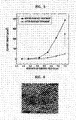
- FIG. 5 is a graph illustrating an electric field emission characteristic of a carbon nanotube emitter, before and after surface treatment, according to another exemplary embodiment of the present invention. Referring to FIG. 5, the electric field emission characteristic is improved after surface treatment.
- FIG. 6 is a SEM image of a surface of the carbon nanotube emitter after treating the surface according to another exemplary embodiment of the present invention.
- the carbon nanotube emitter has a large number of carbon nanotube protruding from its surface after the surface treatment.
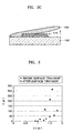
- FIG. 7 is a perspective view illustrating a method of forming a carbon nanotube emitter according to an embodiment of the present invention in FED device.
- FIG. 8 is a cross-sectional view illustrating a method of forming a carbon nanotube emitter according to an embodiment of the present invention in FED device.
- a FED device includes a plurality of carbon nanotube composites 202 and a plurality of gate electrodes 206 disposed on a substrate 200.
- a surface treating material 205 is coated on the carbon nanotube composites 202 and the gate electrodes 206, and dried. Then, a carbon nanotube emitter with improved electric field emission is formed by peeling off the coated surface treating material 205.
- reference numeral 204 denotes an insulating layer.
- a FED device is formed by sequentially stacking a cathode 301, an insulating layer 304, and a gate electrode 306 on a substrate 300.
- a carbon nanotube composite 302 is formed on the cathode 302 inside a hole formed in the insulating layer 304.
- a surface treating material 305 is coated on the gate electrode 306 and the carbon nanotube composite 302. Since the surface treating material 305 is in a liquid phase, it can be well coated on the carbon nanotube composite 302 inside the hole.
- FIG. 9 is a SEM image of the FED device depicted in FIG. 8, a surface of which is coated with the surface treatment material 305. Then, a carbon nanotube emitter that has improved electric field emission is formed after drying and peeling off the coated surface treating material 305.
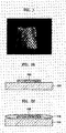
- FIG. 10 is a photographed image of light emitted by the FED depicted in FIG. 7 after a surface of which has been treated.
- FIG. 11 is a photographed image of light emitted by the FED depicted in FIG. 8 after a surface of which has been treated. Referring to FIGS. 10 and 11, uniform light emission is achieved.
- a method of forming a carbon nanotube emitter provides a carbon nanotube emitter that has improved electric field emission by forming a large number of carbon nanotube vertically protruding from the surface of the carbon nanotube emitter by coating a surface treating material in a liquid phase on the carbon nanotube composite and peeling the surface treating material off. Also, the method of forming the carbon nanotube emitter can be applied to a variety of structure devices which include a carbon nanotube emitter since the method of forming carbon nanotube according to the present invention uses a surface treating material in a liquid phase.
Landscapes
- Engineering & Computer Science (AREA)
- Chemical & Material Sciences (AREA)
- Nanotechnology (AREA)
- Manufacturing & Machinery (AREA)
- Physics & Mathematics (AREA)
- Composite Materials (AREA)
- Condensed Matter Physics & Semiconductors (AREA)
- General Physics & Mathematics (AREA)
- Materials Engineering (AREA)
- Crystallography & Structural Chemistry (AREA)
- Organic Chemistry (AREA)
- Inorganic Chemistry (AREA)
- Cold Cathode And The Manufacture (AREA)
- Carbon And Carbon Compounds (AREA)
Abstract
Description
Claims (20)
- A method of forming a carbon nanotube emitter, comprising:forming a carbon nanotube composite (102) on a substrate (100) with a predetermined shape;coating a surface treating material (105) in a liquid phase on the carbon nanotube composite (102) and drying the surface treating material, the surface treating material including an organic polymer binder and an inorganic compound; andpeeling the dried surface treating material off from the carbon nanotube composite.
- The method according to claim 1, wherein the organic polymer binder includes at least one selected from polyvinyl alcohol, polyvinyl acetate, and polyvinyl pyrrolidone.
- The method according to claim 1 or 2, wherein the concentration of the organic polymer binder in the surface treating material is 5 to 20 %wt.
- The method according to any of claims 1 to 3, wherein the inorganic compound includes at least one selected from TiO2, SiO2, and Al2O3.
- The method according to any of claims 1 to 4, wherein the concentration of the inorganic compound in the surface treating material is 3 to 10 %wt.
- The method according to any of claims 1 to 5, wherein the particle size of the inorganic compound is 1 nm to 5 µm.
- The method according to claim 6, wherein the particle size of the inorganic compound is 10 nm to 1 µm.
- The method according to any of claims 1 to 7, wherein the viscosity of the surface treating material is 100 to 5,000 centipoise.
- The method according to any of claims 1 to 8, wherein the forming the carbon nanotube composite comprises:coating a carbon nanotube paste including carbon nanotube, an organic binder, an inorganic binder, and a metal powder on a substrate;patterning the carbon nanotube paste to a predetermined shape; andremoving the organic binder by baking the patterned carbon nanotube paste.
- The method according to claim 9, wherein the organic binder includes a monomer, an oligomer, and a photoinitiator.
- The method according to claim 10, wherein the monomer includes at least one selected from benzyl acrylate, glycidyl methacrylate, phenoxyethyl acrylate, 2(2-ethoxy)ethyl acrylate, 2-ethylhexyl acrylate, and trimethylolpropane triacrylate.
- The method according to claim 10 or 11, wherein the oligomer includes at least one selected from polyester acrylate, epoxy acrylate, and urethane acrylate.
- The method according to any of claims 10 to 12, wherein the photoinitiator includes at least one selected from benzyl dimethylketam, benzoin normal butylether, and alpha-hydroxy keton.
- The method according to any of claims 9 to 13, wherein the inorganic binder includes a glass frit including PbO-ZnO-B2O3.
- The method according to any of claims 9 to 14, wherein the metal powder includes at least one selected from aluminum, silver, zinc, copper, nickel, and iron.
- The method according to any of claims 9 to 15, wherein the carbon nanotube paste is hardened by ultraviolet ray and patterned.
- The method according to any of claims 9 to 16, wherein the organic binder of the carbon nanotube paste is removed by baking at a temperature of 400 to 500 °C.
- A method of forming a carbon nanotube emitter, comprising forming a carbon nanotube composite (102) on a substrate (100) with a predetermined shape;coating a surface treating material (105) including a hardening polymer resin on the carbon nanotube composite (102) and hardening the surface treating material; andpeeling the hardened surface treating material (105) off from the carbon nanotube composite.
- The method according to claim 18, wherein the surface treating material is hardened using one selected from the group consisting of ultraviolet rays, hot air, electronic rays, and far infrared rays.
- The method according to claim 19, wherein, when the surface treating material is hardened by the ultraviolet rays, the surface treating material includes at least one selected from the group consisting of epoxy acrylate, urethane acrylate, ester acrylate, ether acrylate, and acrylic acrylate.
Applications Claiming Priority (2)
| Application Number | Priority Date | Filing Date | Title |
|---|---|---|---|
| KR1020030091870A KR20050060287A (en) | 2003-12-16 | 2003-12-16 | Method for forming carbon nanotube emitter |
| KR2003091870 | 2003-12-16 |
Publications (3)
| Publication Number | Publication Date |
|---|---|
| EP1553613A2 true EP1553613A2 (en) | 2005-07-13 |
| EP1553613A3 EP1553613A3 (en) | 2005-07-20 |
| EP1553613B1 EP1553613B1 (en) | 2007-11-28 |
Family
ID=34588109
Family Applications (1)
| Application Number | Title | Priority Date | Filing Date |
|---|---|---|---|
| EP04256677A Expired - Lifetime EP1553613B1 (en) | 2003-12-16 | 2004-10-28 | Method of forming carbon nanotube emitter |
Country Status (6)
| Country | Link |
|---|---|
| US (1) | US7678424B2 (en) |
| EP (1) | EP1553613B1 (en) |
| JP (1) | JP2005183370A (en) |
| KR (1) | KR20050060287A (en) |
| CN (1) | CN100552857C (en) |
| DE (1) | DE602004010358T2 (en) |
Cited By (3)
| Publication number | Priority date | Publication date | Assignee | Title |
|---|---|---|---|---|
| EP2096659A1 (en) * | 2008-02-29 | 2009-09-02 | Korea University Industry & Academy Cooperation Foundation | Electron emission source, electric device using the same, and method of manufacturing the electron emission source |
| EP1957397A4 (en) * | 2005-12-06 | 2009-09-09 | Korea Electronics Telecomm | METHOD OF MANUFACTURING A CARBON NANOPHONE (CNT) PASTE AND MEMBER WITH HIGH RELIABILITY |
| EP1930933A3 (en) * | 2006-12-07 | 2009-12-09 | Electronics And Telecommunications Research Institute | Method of manufacturing fine patternable carbon nano-tube emitter with high reliability |
Families Citing this family (27)
| Publication number | Priority date | Publication date | Assignee | Title |
|---|---|---|---|---|
| US7449081B2 (en) | 2000-06-21 | 2008-11-11 | E. I. Du Pont De Nemours And Company | Process for improving the emission of electron field emitters |
| US6723299B1 (en) | 2001-05-17 | 2004-04-20 | Zyvex Corporation | System and method for manipulating nanotubes |
| JP2003168355A (en) * | 2001-11-30 | 2003-06-13 | Sony Corp | Method of manufacturing electron emitter, method of manufacturing cold cathode field emission device, and method of manufacturing cold cathode field emission display |
| US20040034177A1 (en) | 2002-05-02 | 2004-02-19 | Jian Chen | Polymer and method for using the polymer for solubilizing nanotubes |
| US6905667B1 (en) | 2002-05-02 | 2005-06-14 | Zyvex Corporation | Polymer and method for using the polymer for noncovalently functionalizing nanotubes |
| US7479516B2 (en) | 2003-05-22 | 2009-01-20 | Zyvex Performance Materials, Llc | Nanocomposites and methods thereto |
| KR20050106670A (en) * | 2004-05-06 | 2005-11-11 | 삼성에스디아이 주식회사 | Manufacturing method of carbon nano tube field emission device |
| US7296576B2 (en) | 2004-08-18 | 2007-11-20 | Zyvex Performance Materials, Llc | Polymers for enhanced solubility of nanomaterials, compositions and methods therefor |
| CN100446155C (en) * | 2005-02-07 | 2008-12-24 | 中山大学 | Preparation method and application of printable nanomaterial cold cathode slurry and field emission cold cathode |
| KR100747332B1 (en) * | 2005-11-28 | 2007-08-07 | 엘지전자 주식회사 | Manufacturing method of field emission display device |
| US20080299298A1 (en) * | 2005-12-06 | 2008-12-04 | Electronics And Telecommunications Research Institute | Methods of Manufacturing Carbon Nanotube (Cnt) Paste and Emitter with High Reliability |
| US7514116B2 (en) * | 2005-12-30 | 2009-04-07 | Intel Corporation | Horizontal Carbon Nanotubes by Vertical Growth and Rolling |
| US8264137B2 (en) * | 2006-01-03 | 2012-09-11 | Samsung Electronics Co., Ltd. | Curing binder material for carbon nanotube electron emission cathodes |
| JP2007188686A (en) * | 2006-01-11 | 2007-07-26 | Togen Denki Kofun Yugenkoshi | Method for activating the electron emission surface of a field emission display device |
| WO2007105707A1 (en) * | 2006-03-13 | 2007-09-20 | Nikon Corporation | Process for production of carbon nanotube aggregates, carbon nanotube aggregates, catalyst particle dispersion membrane, electron emitters, and field emission displays |
| US8052855B2 (en) * | 2006-05-11 | 2011-11-08 | Samsung Electronics Co., Ltd. | Carbon nanotube gas sensor and method of manufacturing the same |
| CN100583354C (en) * | 2006-07-07 | 2010-01-20 | 清华大学 | Method for manufacturing carbon nanotube filament cathode body |
| JP5069486B2 (en) * | 2007-03-14 | 2012-11-07 | 昭和電工株式会社 | Thin film type electron emission material, method for manufacturing the same, field emission type device, and field emission type display |
| TW200934662A (en) * | 2007-12-28 | 2009-08-16 | Du Pont | Method for reworking adhesively bonded liquid crystal displays |
| US8318049B2 (en) * | 2008-09-30 | 2012-11-27 | Samsung Electronics Co., Ltd. | Composition for forming electron emission source, electron emission source including the composition, method of preparing the electron emission source, and field emission device including the electron emission source |
| CN102013371B (en) * | 2009-09-04 | 2012-11-21 | 清华大学 | Surface treatment method for cold cathode |
| TWI407485B (en) * | 2009-09-22 | 2013-09-01 | Hon Hai Prec Ind Co Ltd | Method for treating surface of cold cathode |
| RU2504858C2 (en) * | 2011-07-07 | 2014-01-20 | Российская Федерация, от имени которой выступает Министерство промышленности и торговли РФ | Field-emission cathode |
| KR101337958B1 (en) * | 2012-02-07 | 2013-12-09 | 현대자동차주식회사 | Electromagnetic wave shielding composite and manufacturing method for thereof |
| CN105448624B (en) * | 2014-07-10 | 2017-09-01 | 清华大学 | The preparation method of field-transmitting cathode |
| EP3933881A1 (en) | 2020-06-30 | 2022-01-05 | VEC Imaging GmbH & Co. KG | X-ray source with multiple grids |
| US12230468B2 (en) | 2022-06-30 | 2025-02-18 | Varex Imaging Corporation | X-ray system with field emitters and arc protection |
Family Cites Families (17)
| Publication number | Priority date | Publication date | Assignee | Title |
|---|---|---|---|---|
| US5091251A (en) * | 1989-05-29 | 1992-02-25 | Tomoegawa Paper Co., Ltd. | Adhesive tapes and semiconductor devices |
| JPH04295827A (en) * | 1991-03-25 | 1992-10-20 | Toppan Printing Co Ltd | Production of varistor element |
| JPH05329942A (en) * | 1992-06-01 | 1993-12-14 | Nippon Paint Co Ltd | Method of forming three-dimensional matter by photo-setting resin liquid |
| DE60017117D1 (en) * | 1999-04-23 | 2005-02-03 | Foto Wear Inc | COATED TRANSMISSION SHEET WITH HEAT- AND / OR UV-HARDENABLE MATERIAL |
| CA2409731A1 (en) * | 2000-05-05 | 2001-11-15 | National Starch And Chemical Investment Holding Corporation | Aqueous adhesive formulations |
| US7449081B2 (en) * | 2000-06-21 | 2008-11-11 | E. I. Du Pont De Nemours And Company | Process for improving the emission of electron field emitters |
| JP2002121520A (en) * | 2000-10-05 | 2002-04-26 | Saehan Ind Inc | Adhesive tape for electronic part |
| JP5055655B2 (en) * | 2000-11-20 | 2012-10-24 | 日本電気株式会社 | Emitter manufacturing method, field emission cold cathode using the emitter, and flat image display device |
| KR100416141B1 (en) * | 2001-06-22 | 2004-01-31 | 삼성에스디아이 주식회사 | Method of manufacturing for field emission display having carbon-based emitter |
| JP3654236B2 (en) * | 2001-11-07 | 2005-06-02 | 株式会社日立製作所 | Electrode device manufacturing method |
| JP3493606B2 (en) * | 2001-11-08 | 2004-02-03 | 帝国インキ製造株式会社 | Insert molding products and colored inks for insert molding products |
| JP2003168355A (en) * | 2001-11-30 | 2003-06-13 | Sony Corp | Method of manufacturing electron emitter, method of manufacturing cold cathode field emission device, and method of manufacturing cold cathode field emission display |
| JP2003255403A (en) * | 2002-03-05 | 2003-09-10 | Ricoh Co Ltd | Display medium, display device, display method, and display body |
| KR100852690B1 (en) * | 2002-04-22 | 2008-08-19 | 삼성에스디아이 주식회사 | Carbon nanotube emitter paste composition for field emission display device and manufacturing method of carbon nanotube emitter for field emission display device using same |
| US7317277B2 (en) * | 2002-04-24 | 2008-01-08 | E.I. Du Pont De Nemours And Company | Electron field emitter and compositions related thereto |
| US6798127B2 (en) * | 2002-10-09 | 2004-09-28 | Nano-Proprietary, Inc. | Enhanced field emission from carbon nanotubes mixed with particles |
| US7303854B2 (en) * | 2003-02-14 | 2007-12-04 | E.I. Du Pont De Nemours And Company | Electrode-forming composition for field emission type of display device, and method using such a composition |
-
2003
- 2003-12-16 KR KR1020030091870A patent/KR20050060287A/en not_active Withdrawn
-
2004
- 2004-10-28 EP EP04256677A patent/EP1553613B1/en not_active Expired - Lifetime
- 2004-10-28 DE DE602004010358T patent/DE602004010358T2/en not_active Expired - Lifetime
- 2004-10-29 CN CNB2004100896472A patent/CN100552857C/en not_active Expired - Fee Related
- 2004-11-19 US US10/992,333 patent/US7678424B2/en not_active Expired - Fee Related
- 2004-11-24 JP JP2004339542A patent/JP2005183370A/en not_active Ceased
Cited By (6)
| Publication number | Priority date | Publication date | Assignee | Title |
|---|---|---|---|---|
| EP1957397A4 (en) * | 2005-12-06 | 2009-09-09 | Korea Electronics Telecomm | METHOD OF MANUFACTURING A CARBON NANOPHONE (CNT) PASTE AND MEMBER WITH HIGH RELIABILITY |
| EP1930933A3 (en) * | 2006-12-07 | 2009-12-09 | Electronics And Telecommunications Research Institute | Method of manufacturing fine patternable carbon nano-tube emitter with high reliability |
| US7887878B2 (en) | 2006-12-07 | 2011-02-15 | Electronics And Telecommunications Research Institute | Method of manufacturing a fine-patternable, carbon nano-tube emitter with high reliabilty |
| TWI383419B (en) * | 2006-12-07 | 2013-01-21 | Korea Electronics Telecomm | Method of manufacturing fine patternable carbon nano-tube emitter with high reliability |
| EP2096659A1 (en) * | 2008-02-29 | 2009-09-02 | Korea University Industry & Academy Cooperation Foundation | Electron emission source, electric device using the same, and method of manufacturing the electron emission source |
| US8513870B2 (en) | 2008-02-29 | 2013-08-20 | Korea University Industrial & Academic Cooperation Foundation | Electron emission source, electric device using the same, and method of manufacturing the electron emission source |
Also Published As
| Publication number | Publication date |
|---|---|
| US20050129858A1 (en) | 2005-06-16 |
| EP1553613A3 (en) | 2005-07-20 |
| DE602004010358T2 (en) | 2008-10-02 |
| JP2005183370A (en) | 2005-07-07 |
| CN100552857C (en) | 2009-10-21 |
| DE602004010358D1 (en) | 2008-01-10 |
| US7678424B2 (en) | 2010-03-16 |
| CN1630002A (en) | 2005-06-22 |
| EP1553613B1 (en) | 2007-11-28 |
| KR20050060287A (en) | 2005-06-22 |
Similar Documents
| Publication | Publication Date | Title |
|---|---|---|
| EP1553613B1 (en) | Method of forming carbon nanotube emitter | |
| US9034212B2 (en) | Composition for forming electron emission source, electron emission source including the composition, method of preparing the electron emission source, and field emission device including the electron emission source | |
| US7887878B2 (en) | Method of manufacturing a fine-patternable, carbon nano-tube emitter with high reliabilty | |
| US20040195950A1 (en) | Field emission display including electron emission source formed in multi-layer structure | |
| KR20030059291A (en) | Pattern forming method for carbon nanotube, and field emission cold cathode and method of manufacturing the cold cathode | |
| JP2004504690A (en) | Method for improving the emission state of an electron field emitter | |
| US7662428B2 (en) | Method for carbon nanotube emitter surface treatment | |
| KR100670330B1 (en) | An electron emission source and an electron emission device comprising the electron emission source | |
| US7615917B2 (en) | Electron emission source, method of preparing the same, and electron emission device employing the electron emission source | |
| CN1828802B (en) | Electron emission source, manufacturing method thereof, and electron emission device using the same | |
| US7795794B2 (en) | Electron emission source, electron emission device using the same, and composition for the same | |
| JP2009117360A (en) | Boron nitride nanotube paste composition, electron emission source manufactured using the same, electron emission device including the electron emission source, backlight device and electron emission display device to which the electron emission device is applied | |
| US6815238B2 (en) | Method of manufacturing field emission device | |
| KR100762590B1 (en) | Field emission type display device using carbon nanotube and manufacturing method thereof | |
| KR100932976B1 (en) | Slurry composition for electron emission source formation of flat panel display device and electrode formation method using same | |
| KR101166014B1 (en) | A composition for preparing an electron emitter, the electron emitter prepared using the composition, and an electron emission device comprising the electron emitter | |
| US20070164657A1 (en) | Method of manufacturing electron emission device, electron emission device manufactured using the method, and backlight unit and electron emission display device employing electron emission device | |
| KR101166015B1 (en) | An electron emission source, a composition for preparing an electron emission source, a method for preparing the electron emission source and an electron emission device comprising the electron emission source | |
| KR101100820B1 (en) | A composition for forming an electron emission source, an electron emission source manufactured using the same, and an electron emission device including the electron emission source | |
| KR101100819B1 (en) | A composition for forming an electron emission source, an electron emission source manufactured using the same, and an electron emission device including the electron emission source | |
| KR101100814B1 (en) | A composition for forming an electron emission source, an electron emission source manufactured using the same, and an electron emission device including the electron emission source | |
| KR100647439B1 (en) | Manufacturing method of nano carbon field emitter for electron emission | |
| KR20060019911A (en) | Electron emitting device comprising a method of manufacturing an electron emitting source through a plasma treatment and an electron emitting source | |
| KR20070084918A (en) | A composition for forming an electron emission source, an electron emission source manufactured using the same, an electron emission device including the electron emission source, and a method of manufacturing the electron emission source | |
| KR20060054545A (en) | A composition for forming an electron emission source, an electron emission source manufactured using the same, and an electron emission device including the electron emission source |
Legal Events
| Date | Code | Title | Description |
|---|---|---|---|
| PUAI | Public reference made under article 153(3) epc to a published international application that has entered the european phase |
Free format text: ORIGINAL CODE: 0009012 |
|
| PUAL | Search report despatched |
Free format text: ORIGINAL CODE: 0009013 |
|
| 17P | Request for examination filed |
Effective date: 20041117 |
|
| AK | Designated contracting states |
Kind code of ref document: A2 Designated state(s): AT BE BG CH CY CZ DE DK EE ES FI FR GB GR HU IE IT LI LU MC NL PL PT RO SE SI SK TR |
|
| AX | Request for extension of the european patent |
Extension state: AL HR LT LV MK |
|
| AK | Designated contracting states |
Kind code of ref document: A3 Designated state(s): AT BE BG CH CY CZ DE DK EE ES FI FR GB GR HU IE IT LI LU MC NL PL PT RO SE SI SK TR |
|
| AX | Request for extension of the european patent |
Extension state: AL HR LT LV MK |
|
| AKX | Designation fees paid |
Designated state(s): DE FR GB |
|
| GRAP | Despatch of communication of intention to grant a patent |
Free format text: ORIGINAL CODE: EPIDOSNIGR1 |
|
| RIN1 | Information on inventor provided before grant (corrected) |
Inventor name: LEE, HYUN-JUNG,805-502 YEOLMAE MAEUL SAEMIRAE APT Inventor name: MOON, JONG-WOON Inventor name: CHUNG, DEUK-SEOK,218-1509 SIBEOM-DANJI WOOSUNG AP Inventor name: JIN, YONG-WAN Inventor name: CHOI, JUN-HEE,248-1901 SSANGYONG APT. Inventor name: CHO, SUNG-HEE,102-407 DONGA GREEN APT. |
|
| GRAS | Grant fee paid |
Free format text: ORIGINAL CODE: EPIDOSNIGR3 |
|
| GRAA | (expected) grant |
Free format text: ORIGINAL CODE: 0009210 |
|
| AK | Designated contracting states |
Kind code of ref document: B1 Designated state(s): DE FR GB |
|
| REG | Reference to a national code |
Ref country code: GB Ref legal event code: FG4D |
|
| RIN1 | Information on inventor provided before grant (corrected) |
Inventor name: CHOI, JUN-HEE,248-1901 SSANGYONG APT. Inventor name: JIN, YONG-WAN Inventor name: CHO, SUNG-HEE,102-407 DONGA GREEN APT. Inventor name: LEE, HYUN-JUNG,805-502 YEOLMAE MAEUL SAEMIRAE APT Inventor name: MOON, JONG-WOON Inventor name: CHUNG, DEUK-SEOK,218-1509 SIBEOM-DANJI WOOSUNG AP |
|
| REF | Corresponds to: |
Ref document number: 602004010358 Country of ref document: DE Date of ref document: 20080110 Kind code of ref document: P |
|
| ET | Fr: translation filed | ||
| PLBE | No opposition filed within time limit |
Free format text: ORIGINAL CODE: 0009261 |
|
| STAA | Information on the status of an ep patent application or granted ep patent |
Free format text: STATUS: NO OPPOSITION FILED WITHIN TIME LIMIT |
|
| 26N | No opposition filed |
Effective date: 20080829 |
|
| PGFP | Annual fee paid to national office [announced via postgrant information from national office to epo] |
Ref country code: GB Payment date: 20130926 Year of fee payment: 10 |
|
| PGFP | Annual fee paid to national office [announced via postgrant information from national office to epo] |
Ref country code: FR Payment date: 20130926 Year of fee payment: 10 Ref country code: DE Payment date: 20131003 Year of fee payment: 10 |
|
| REG | Reference to a national code |
Ref country code: DE Ref legal event code: R119 Ref document number: 602004010358 Country of ref document: DE |
|
| GBPC | Gb: european patent ceased through non-payment of renewal fee |
Effective date: 20141028 |
|
| PG25 | Lapsed in a contracting state [announced via postgrant information from national office to epo] |
Ref country code: DE Free format text: LAPSE BECAUSE OF NON-PAYMENT OF DUE FEES Effective date: 20150501 Ref country code: GB Free format text: LAPSE BECAUSE OF NON-PAYMENT OF DUE FEES Effective date: 20141028 |
|
| REG | Reference to a national code |
Ref country code: FR Ref legal event code: ST Effective date: 20150630 |
|
| PG25 | Lapsed in a contracting state [announced via postgrant information from national office to epo] |
Ref country code: FR Free format text: LAPSE BECAUSE OF NON-PAYMENT OF DUE FEES Effective date: 20141031 |