EP1551100B1 - Dämpfungseinheit mit einer Vorrichtung zum Steuern des Dämpfungsfaktors - Google Patents
Dämpfungseinheit mit einer Vorrichtung zum Steuern des Dämpfungsfaktors Download PDFInfo
- Publication number
- EP1551100B1 EP1551100B1 EP04368077A EP04368077A EP1551100B1 EP 1551100 B1 EP1551100 B1 EP 1551100B1 EP 04368077 A EP04368077 A EP 04368077A EP 04368077 A EP04368077 A EP 04368077A EP 1551100 B1 EP1551100 B1 EP 1551100B1
- Authority
- EP
- European Patent Office
- Prior art keywords
- electrode
- amplifier
- output
- transistor
- current
- Prior art date
- Legal status (The legal status is an assumption and is not a legal conclusion. Google has not performed a legal analysis and makes no representation as to the accuracy of the status listed.)
- Expired - Lifetime
Links
- XUIMIQQOPSSXEZ-UHFFFAOYSA-N Silicon Chemical compound [Si] XUIMIQQOPSSXEZ-UHFFFAOYSA-N 0.000 description 5
- 238000004519 manufacturing process Methods 0.000 description 5
- 229910052710 silicon Inorganic materials 0.000 description 3
- 239000010703 silicon Substances 0.000 description 3
- 238000006243 chemical reaction Methods 0.000 description 2
- 239000006185 dispersion Substances 0.000 description 2
- 235000021183 entrée Nutrition 0.000 description 2
- 230000010287 polarization Effects 0.000 description 2
- 101100114661 Mus musculus Cep250 gene Proteins 0.000 description 1
- 239000003990 capacitor Substances 0.000 description 1
- 230000007850 degeneration Effects 0.000 description 1
- 238000005516 engineering process Methods 0.000 description 1
- 230000001939 inductive effect Effects 0.000 description 1
- 238000000034 method Methods 0.000 description 1
- 230000000116 mitigating effect Effects 0.000 description 1
- 230000003071 parasitic effect Effects 0.000 description 1
Images




Classifications
-
- H—ELECTRICITY
- H03—ELECTRONIC CIRCUITRY
- H03G—CONTROL OF AMPLIFICATION
- H03G1/00—Details of arrangements for controlling amplification
- H03G1/04—Modifications of control circuit to reduce distortion caused by control
-
- H—ELECTRICITY
- H03—ELECTRONIC CIRCUITRY
- H03G—CONTROL OF AMPLIFICATION
- H03G7/00—Volume compression or expansion in amplifiers
- H03G7/06—Volume compression or expansion in amplifiers having semiconductor devices
Definitions
- the present invention relates to analog signal processing circuits and in particular to an attenuation cell having an attenuation factor control device, linear in dB as a function of a control value, voltage or current.
- the attenuation cell is frequently used in analog signal processing circuits. When associated with an amplifier, it allows for a variable gain as illustrated in FIG. figure 1 where we see a cell 1 combined with an amplifier 2 - transconductance type - which receives a differential input signal V in . By varying the current flowing in the load, composed of two resistors 3 and 4, the gain of the entire circuit is controlled.
- WCDMA Wideband Code Division Multiple Access
- CDMA Code Division Multiple Access
- the present invention relates to an attenuation control circuit for precisely controlling a gain, expressed in decibels, from a setpoint - current or input voltage.
- the attenuation cell which comprises a first differential pair fed by a first current source and a second differential pair fed by a second current source.
- the input of the cell is composed of, on the one hand, commonly connected transmitters of the first pair and, on the other hand, transmitters commonly connected to the second differential pair.
- a gain control device applies a VA - VB potential between the bases of the two differential pairs and comprises a set of three diodes in which a current IA, IB and the sum IA + IB of the two previous currents are respectively traveled.
- the two diodes traversed by a current IB and IA + IB generate a potential, respectively VB and VC, and the difference between these two potentials is used to generate a magnitude Iz used in a control loop.
- a setpoint Vct is transformed into an information lx, then into an information ly proportional to the absolute temperature T, and an error amplifier uses the information ly - lz and generates the currents IA and IB while minimizing this difference.
- all the information lx ly and lz are differential currents and said error amplifier is a current amplifier.
- the figure 1 illustrates the conventional scheme of an attenuation cell associated with an amplifier circuit for achieving a variable gain.
- the figure 2 illustrates the basic architecture of an attenuation cell to which the gain control device according to the invention will be applied.
- the figure 3 illustrates the preferred embodiment of the gain control device according to the invention.
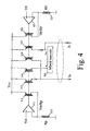
- the figure 4 illustrates the preferred embodiment of the converter circuit 30 of the gain control device according to the invention.
- the figure 5 illustrates the preferred embodiment of the analog multiplier 40 of the gain control device according to the invention.
- the figure 6 illustrates the linear characteristic obtained with the gain control of the attenuation cell.
- the figure 2 illustrates the basic architecture of an attenuation cell to which the gain control according to the invention will be applied.
- This cell consists of two differential pairs of bipolar transistors.
- the first pair comprises a first transistor Q1 21 and a second transistor Q2 22, while the second pair consists of a third transistor Q3 23 and a fourth transistor Q4.
- the common emitter electrode of each pair of transistors Q1-Q2 and Q3-Q4 is biased by a bias current I 0 supplied by a current source, respectively 28 and 29.
- the bases of the transistors Q1 and Q4 are connected together to the same potential A and, likewise, the bases of the transistors Q2 and Q3 are connected to the same potential B.
- the potential difference between the two points A and B is fixed by a control voltage V ctrl , which controls the attenuation applied by the attenuation cell composed of the two differential pairs Q1-Q2 and Q3-Q4.
- the attenuation cell comprises two input electrodes, which consist, on the one hand, of the common emitter electrode of the pair Q1-Q2 and, on the other hand, of the common emitter common electrode of the Q3-Q4 pair.
- the collectors of transistors Q1 and Q4 provide a first and a second output electrode of the attenuation cell, to which will be connected, as seen in FIG. figure 2 , a first resistive load 25 and a second resistive load 26. More generally, it will also be possible to consider charges of the inductive type.
- a differential voltage between the two bases of the attenuation cell creates a current bypass between the emitters of the two differential pairs Q1-Q2 and Q3-Q4 as illustrated in FIG. figure 2 by the current source I in .
- This current I in is the input current of the attenuation cell from, e.g., a transconductance amplifier such as that illustrated in figure 1 .
- lin is thus or completely switched in Q1 (respectively Q4), or completely in Q2 (respectively Q3), or partially in Q1 or Q2, ensuring different attenuation levels for the current I1rf (respectively l2rf).
- the attenuation factor of the cell which will be designated by the generic expression of gain (even when this is less than 1) is a a magnitude which is directly homothetic of the ratio of the polarization currents of the transistors, which makes it possible to express the gain in decibel in the following form:
- Have dB 20 log l Q ⁇ 1 / l 0
- the figure 3 illustrates the control circuit of the attenuation factor of the cell described in the figure 2 , and in particular the generation of the base control potentials A and B of the transistors Q1-Q4 and Q2-Q3.
- the control circuit comprises a converter circuit 30 receiving a setpoint analog quantity, for example a voltage or a current used to linearly control the attenuation factor of the cell.
- the setpoint is in the form of a potential Vct that the converter circuit 30 converts in the form of a differential current Ix.
- all electrical quantities are converted into a differential current, which greatly simplifies the design of the servo circuit and increases, moreover, the accuracy of the control of the attenuation factor .
- the differential current Ix generated by the circuit 30 is then transmitted to an analog multiplier 40, which multiplies the current Ix generated by the amplifier 30 by a magnitude I ptat / I 0 proportional to the temperature ( Proportional To Absolute Temperature PTAT).
- a magnitude I ptat / I 0 proportional to the temperature ( Proportional To Absolute Temperature PTAT).
- the circuit also comprises a set of three transistors 91, 92 and 93 which are mounted in diodes and whose junctions np serves to generate the logarithmic linear conversion allowing the linear control of the attenuation factor expressed in decibels, as represented in FIG. figure 6 .
- a first transistor 91, mounted diode, is traversed by a current IA and has an emitter electrode whose potential VA is transmitted, via a voltage follower 80, to the control potential A of the common bases of transistors Q1-Q4 of the figure 2 .
- a second transistor 92 also diode mounted, is traversed by a current IB and has an emitter electrode whose potential VB is transmitted, via voltage follower 70, to the potential B of the common bases of the transistors Q2-Q3 of the figure 2 .
- the elements 70 and 80 serve to ensure that the bases of transistors Q2-Q3 and Q1-Q4, respectively, do not disturb the accuracy of the mechanism enslavement of the figure 3 . This makes it possible to control high levels of attenuation.
- a third bipolar transistor QC 93 also diode-mounted, and in which the sum of the two currents IA + IB is generated, generated by a current source 94.
- the electrode of FIG. emitter of this transistor 93 generates a potential VC which is transmitted to a first input of an amplifier circuit 60 whose second input receives the emitter potential of the transistor QB 92.
- the potential difference VB-VC is thus directly transmitted to the amplifier 60, which is strongly degenerated to ensure good linearity, and the emitter potentials of the transistors 91 and 93 are thus used in the servocontrol loop of the control circuit. gain. Indeed, the amplifier 60 receives these two potentials at its two inputs and generates from the ddp between the points B and C a differential current Iz, which, as can be seen in FIG. figure 3 , is found subtracted from the set differential current Iy generated by the multiplier 40.
- the difference ly-Iz is then used as an error quantity which is transmitted to an error amplifier 50, which generates the currents IA and IB so as to reduce the size ly-Iz to zero.
- the error amplifier 50 generates the currents IA, IB and also the current IA + IB which flows in the third transistor 93.
- a differential control loop of the attenuation factor of the attenuation cell is thus obtained. No mathematical approximation is made and it is found that the control loop provides a high accuracy of the gain control.
- the servocontrolling performed by the error amplifier 50 makes it possible to compensate precisely the temperature dependence phenomena of the diode junctions 91-93.
- the insensitivity to temperature that is obtained by generating a setpoint proportional to the absolute temperature achieves an accuracy greater than 1 dB for a temperature range of 125 degrees.
- the figure 4 illustrates the preferred embodiment of the voltage-current converter circuit 30.
- the latter comprises two amplifiers 311 and 321 each having a non-inverting input connected respectively to a reference voltage V ct and a reference voltage V 0 .
- Amplifiers 311 and 321 each have an inverting input which is connected to ground via a resistor Rp and R0 respectively. They furthermore each comprise an output electrode, which is connected to the gate of a set of three MOS transistors, 312-313-314 and 324-323-322 respectively. The source electrode of all the transistors is connected to the positive potential Vcc.
- the transistor 312 (or 322) has a drain which is connected to the inverting input of the amplifier 311 (respectively 321).
- the drain of the transistor 313 is connected to the drain of the transistor 324 and also to a first output electrode of the converter circuit 30.
- the drain of the transistor 314 is connected to an input of a cascode mirror circuit 301, an output of which is connected to the drain of the transistor 323 and also to a second output electrode of the converter circuit 30.
- the operation of the circuit 30 is as follows: the combination of the MOS transistor 312 and the amplifier 311 makes it possible to generate a current V ct / R p which flows in the transistor 313 (mounted in current mirror with respect to the transistor 312).
- the combination of the MOS transistor 322 and the amplifier 321 generates a current V 0 / R 0 flowing in the transistor 323.
- the transistor 324 also mounted in current mirror, makes it possible to generate a replica of this current. V0 / R0 which adds to the current V ct / R p .
- the two output electrodes of the circuit 30 are thus circulating a current V 0 / R 0 + V ct / R p and V 0 / R 0 - V ct / R p respectively.
- the differential current conversion is thus carried out. It should be noted that the generation of currents must be carried out with great precision.
- the resistors will have precise values and the MOS transistors will preferably be large-area transistors in order to reduce offset voltages (Offset). In the same way, the offset voltage of the amplifiers 311 and 321 will be reduced.
- a reference potential independent of the temperature will be chosen, which can be achieved by means of a reference of the type Gap tape.
- the figure 5 illustrates the preferred embodiment of the analog multiplier 40.
- the multiplier comprises two input transistors 415 and 405 whose collector electrode respectively receives the currents V 0 / R 0 + V ct / R p and V 0 / R 0 - V ct / R p generated at the output of the converter 30.
- the emitter electrode of the two transistors 415 and 405 is connected via a resistor R4 401 to ground.
- the multiplier 40 further comprises two output transistors 411 and 412 respectively traversed by a current Inm and Inp which is transmitted via the collector to one of the output electrodes of the multiplier, respectively 450 and 440.
- the emitter of each of the transistors 411 and 412 is connected to a resistor R1 404 whose other electrode is connected to ground.
- the multiplier further comprises two transistors 410 and 413 traversed by a copy current Inmc and Inmp, respectively, and which have a common emitter electrode connected to the mass via the same resistor R2 403.
- Two buffer type MOS transistors 406 and 416 have a gate connected respectively to the electrode 420 and 430 and have their drain electrodes connected together.
- the source of the transistor 406 is connected to the bases of the transistors 405, 409, 410 and 411 while the source of the transistor 416 is connected to the bases of the transistors 412, 413, 414 and 415.
- Two capacitors 407 and 417, respectively connected between gate and source of transistors 406 and 407 are used to stabilize the operation of these same transistors.
- An MOS transistor 408 has a gate connected to the electrode 480 receiving a reference current Ibias, and a drain connected to the common drains of the transistors 406 and 417. Its source is connected to the resistor 401.
- the set of transistors 408, 409, 414 and 402 ensures the polarization of all transistors 405, 410, 411, 412, 413 and 415 by allowing a low voltage on the emitters of transistors 405, 409, 410, 411, 412, 413, 414 and 417, typically 100 mV. If one had a current source in place of transistors 402, 403 and 304, it would have had about 400mV minimum. As can be seen this circuit makes it possible to carry out a stack, under low voltage (2.5 Volt minimum) of the function 50 above the function 40.
- I 1 is a PTAT current made by a conventional circuit. It can thus be seen that the absolute datum Vct / V0 can be transformed into a quantity which is ptat I 1 .
- This current can then be directly used in the feedback loop of the figure 3 to generate the error ly - lz used by the error amplifier 50.
- the error amplifier 50 is used to generate the currents IA, IB and IA + IB which flow in the diodes 91, 92 and 93.
Landscapes
- Amplifiers (AREA)
- Control Of Amplification And Gain Control (AREA)
- Networks Using Active Elements (AREA)
- Attenuators (AREA)
- Fluid-Damping Devices (AREA)
- Vibration Prevention Devices (AREA)
Claims (4)
- Dämpfungsglied mit einer Vorrichtung zur Steuerung des Dämpfungsfaktors, wobei das besagte Dämpfungsglied eine erste und eine zweite Eingangselektrode (A, B) sowie eine erste und eine zweite Ausgangselektrode besitzt,- wobei ein erstes Differentialpaar einen ersten bipolaren Transistor (21) und einen zweiten bipolaren Transistor (22) besitzt, wobei der erste und zweite bipolare Transistor jeweils eine Emitterelektrode besitzen, die an ein und dieselbe erste Stromquelle (28) sowie an die besagte erste Eingangselektrode angeschlossen sind, wobei der besagte erste Transistor (21) einen Kollektor besitzt, der an die besagte erste Ausgangselektrode angeschlossen ist,- wobei ein zweites Differentialpaar einen dritten bipolaren Transistor (23) und einen vierten bipolaren Transistor (24) besitzt, wobei der dritte und vierte bipolare Transistor je eine Sendelektrode besitzen, die an eine zweite Stromquelle (29) sowie an die besagte zweite Eingangselektrode angeschlossen sind, während der besagte vierte Transistor (24) einen Kollektor besitzt, der an die besagte zweite Ausgangselektrode angeschlossen ist,wobei der erste und der vierte bipolare Transistor (21, 24) eine Basis besitzen, die an ein und dasselbe Potential VA angeschlossen sind, während der zweite und der dritte bipolare Transistor (22, 23) eine Basis besitzen, die an ein und dasselbe Potential VB angeschlossen sind,
wobei die Vorrichtung zur Steuerung des Dämpfungsfaktors, mit dem jeweils die Potentiale VA und VB festgelegt werden,- eine erste Diode (91) besitzt, in der ein Strom IA so fließt, dass eine Potentialdifferenz gebildet wird, durch die das besagte Potential VA gesteuert wird,- eine zweite Diode (92) besitzt, in der ein Strom IB so fließt, dass eine Potentialdifferenz gebildet wird, durch die das besagte Potential VB gesteuert wird,dadurch gekennzeichnet, dass es weiterhin- eine dritte Diode (93) besitzt, in der die Summe IA + IB der in der ersten und zweiten Diode (91, 92) fließenden Ströme fließt, die von einer Stromquelle erzeugt werden, so dass eine Potentialdifferenz VC gebildet wird, die der Summe der Ströme IA + IB entspricht,- einen Verstärker (60) besitzt, der über zwei Eingänge verfügt, die jeweils an die durch die zweite Diode (92) und die dritte Diode (93) erzeugten Potentiale VR und VC angeschlossen sind, wobei der besagte Verstärker (60) eine Information lz erzeugt, die repräsentativ für die Differenz zwischen den Potentialen VB und VC ist,- eine Wandlerschaltung (30) besitzt, die einen Vorgabewert Vct aufnimmt, durch den eine erste elektrische Zwischengröße lx erzeugt wird,- eine Vervielfachungsschaltung (40) besitzt, die die besagte erste Zwischengröße und eine zweite elektrische Größe aufnimmt, die proportional zur absoluten Temperatur ist, während die besagte Vervielfachungsschaltung eine zweite Größe ly erzeugt, die proportional zum besagten Vorgabewert Vct und zur absoluten Temperatur T ist,- einen Fehlerverstärker besitzt, der am Eingang den Fehler ly - 1z aufnimmt und die Ströme IA und IB so erzeugt, dass der besagte Fehler minimal ist. - Dämpfungsglied nach Anspruch 1, dadurch gekennzeichnet, dass die erste und die zweite Größe (lx, ly) und die besagte, vom Verstärker erzeugte Information lz, die die besagten Potentiale VR und VC aufnimmt, Stromstärken sind, während der besagte Fehlerverstärker (50) ein Stromverstärker ist.
- Dämpfungsglied nach Anspruch 2, dadurch gekennzeichnet, dass es Spannungsfolger (70, 80) besitzt, mit denen jeweils die Potentiale VA und VB an die Basen zur Steuerung der Transistoren (21, 22, 23, 24) des besagten Dämpfungsglieds übertragen werden.
- Dämpfungsglied nach Anspruch 2, dadurch gekennzeichnet, dass die Wandlerschaltung (30)- einen ersten und einen zweiten Verstärker (311, 312) besitzt, von denen jeder einen nicht invertierenden Eingang und einen invertierenden Eingang sowie einen Ausgang besitzt,-- wobei der nicht invertierende Eingang des ersten und des zweiten Verstärkers (311, 312) jeweils an eine Spannung von Vct und an eine Referenzspannung V0 angeschlossen ist,-- wobei der invertierende Eingang des ersten und des zweiten Verstärkers (311, 312) über die Widerstände Rp und R0 jeweils an die Masse angeschlossen ist,- einen ersten MOS-Transistor (312) mit einer Gateelektrode, einer Quellenelektrode und einer Drainelektrode besitzt, wobei die besagte Quellenelektrode an das positive Potential Vcc, die besagte Gateelektrode an den Ausgang des besagten ersten Verstärkers 311 und die besagte Drainelektrode an den nicht invertierenden Eingang des besagten ersten Verstärkers 311 angeschlossen ist- einen zweiten MOS-Transistor (313) mit einer Gateelektronde, einer Quellenelektrode und einer Drainelektrode besitzt, wobei die besagte Quellenelektrode an das positive Potential Vcc, die besagte Gateelektrode an den Ausgang des besagten ersten Verstärkers 311 und die besagte Drainelektrode an einen ersten Ausgang der Wanderschaltung (30) angeschlossen ist,- einen dritten MOS-Transistor (314) mit einer Gateelektrode, einer Quellenelektrode und einer Drainelektrode besitzt, wobei die besagte Quellenelektrode an das positive Potential Vcc, die besagte Gateelektrode an den Ausgang des besagten ersten Verstärkers 311 und die besagte Drainelektrode an einen Eingang einer Kaskode-Stromspiegelschaltung (301) angeschlossen ist,- einen vierten MOS-Transistor (322) mit einer Gateelektrode, einer Quellenelektrode und einer Drainelektrode besitzt, wobei die besagte Quellenelektrode an das positive Potential Vcc, die besagte Gateelektrode an den Ausgang des besagten zweiten Verstärkers 321 und die besagte Drainelektrode an den nicht invertierenden Eingang des besagten ersten Verstärkers 321 angeschlossen ist,- einen fünften MOS-Transistor (323) mit einer Gateelektrode, einer Quellenelektrode und einer Drainelektrode besitzt, wobei die besagte Quellenelektrode an das positive Potential Vcc, die besagte Gateelektrode an den Ausgang des besagten zweiten Verstärkers 321 und die besagte Drainelektrode an einen Ausgang der besagten Kaskodcnschaltung (301) sowie an einen zweiten Ausgang der Wandlerschaltung (30) angeschlossen ist,- einen sechsten MOS-Transistor (314) mit einer Gateelektrode, einer Quellenelektrode und einer Drainelektrode besitzt, wobei die besagte Ouellenelektrode an das positive Potential Vcc, die besagte Gateelektrode an den Ausgang des besagten zweiten Verstärkers 321 und die besagte Drainelektrode an die Quellenelektrode des besagten zweiten MOS-Transistor (313) angeschlossen ist.
Applications Claiming Priority (2)
| Application Number | Priority Date | Filing Date | Title |
|---|---|---|---|
| FR0315479A FR2864725A1 (fr) | 2003-12-29 | 2003-12-29 | Cellule d'attenuation presentant un dispositif de commande du facteur d'attenuation |
| FR0315479 | 2003-12-29 |
Publications (3)
| Publication Number | Publication Date |
|---|---|
| EP1551100A2 EP1551100A2 (de) | 2005-07-06 |
| EP1551100A3 EP1551100A3 (de) | 2006-02-01 |
| EP1551100B1 true EP1551100B1 (de) | 2008-04-16 |
Family
ID=34566351
Family Applications (1)
| Application Number | Title | Priority Date | Filing Date |
|---|---|---|---|
| EP04368077A Expired - Lifetime EP1551100B1 (de) | 2003-12-29 | 2004-12-28 | Dämpfungseinheit mit einer Vorrichtung zum Steuern des Dämpfungsfaktors |
Country Status (5)
| Country | Link |
|---|---|
| US (1) | US7227412B2 (de) |
| EP (1) | EP1551100B1 (de) |
| AT (1) | ATE392740T1 (de) |
| DE (1) | DE602004013114D1 (de) |
| FR (1) | FR2864725A1 (de) |
Family Cites Families (7)
| Publication number | Priority date | Publication date | Assignee | Title |
|---|---|---|---|---|
| US5757230A (en) * | 1996-05-28 | 1998-05-26 | Analog Devices, Inc. | Variable gain CMOS amplifier |
| US6084471A (en) * | 1997-12-19 | 2000-07-04 | Nokia Mobile Phones | Soft-limiting control circuit for variable gain amplifiers |
| US6124761A (en) * | 1998-09-30 | 2000-09-26 | Robinson; Trevor | Variable gain amplifier with gain linear with control voltage |
| JP3469486B2 (ja) * | 1998-12-25 | 2003-11-25 | 株式会社東芝 | 可変利得回路 |
| JP4073152B2 (ja) * | 2000-06-30 | 2008-04-09 | 富士通株式会社 | 利得可変増幅器 |
| US6456142B1 (en) * | 2000-11-28 | 2002-09-24 | Analog Devices, Inc. | Circuit having dual feedback multipliers |
| FI116870B (fi) * | 2003-06-19 | 2006-03-15 | Nokia Corp | Järjestely energian säästämiseksi lähettimessä sekä radiolaite |
-
2003
- 2003-12-29 FR FR0315479A patent/FR2864725A1/fr not_active Withdrawn
-
2004
- 2004-12-28 DE DE602004013114T patent/DE602004013114D1/de not_active Expired - Lifetime
- 2004-12-28 AT AT04368077T patent/ATE392740T1/de not_active IP Right Cessation
- 2004-12-28 EP EP04368077A patent/EP1551100B1/de not_active Expired - Lifetime
- 2004-12-29 US US11/025,848 patent/US7227412B2/en not_active Expired - Fee Related
Also Published As
| Publication number | Publication date |
|---|---|
| DE602004013114D1 (de) | 2008-05-29 |
| ATE392740T1 (de) | 2008-05-15 |
| US20050195034A1 (en) | 2005-09-08 |
| US7227412B2 (en) | 2007-06-05 |
| EP1551100A3 (de) | 2006-02-01 |
| EP1551100A2 (de) | 2005-07-06 |
| FR2864725A1 (fr) | 2005-07-01 |
Similar Documents
| Publication | Publication Date | Title |
|---|---|---|
| EP0658977B1 (de) | Verstärker mit einstellbarer Verstärkung | |
| FR2623307A1 (fr) | Source de courant a deux bornes avec compensation de temperature | |
| FR2524142A1 (fr) | Circuit integre amplificateur de signal de thermocouple avec compensation de la temperature de soudure froide | |
| EP0424264B1 (de) | Stromquelle mit niedrigem Temperaturkoeffizient | |
| FR2606954A1 (fr) | Amplificateur de puissance operationnel cmos entierement differentiel | |
| EP2095502B1 (de) | Transkonduktanzverstärker mit verbesserter linearität | |
| EP0740425B1 (de) | Genauigkeits-Digital-Analog-Wandler | |
| EP2067090B1 (de) | Spannungsreferenz-elektronikschaltung | |
| FR2529411A1 (fr) | Amplificateur de courant a circuit integre avec amelioration de la linearite et la precision du coefficient de multiplication du circuit | |
| FR2621190A1 (fr) | Amplificateur d'instrumentation a gain programmable | |
| FR2514214A1 (fr) | Circuit a gain variable | |
| FR2607337A1 (fr) | Convertisseur courant-tension | |
| FR2527864A1 (fr) | Circuit de reduction de bruit par compression et expansion du signal | |
| EP1551100B1 (de) | Dämpfungseinheit mit einer Vorrichtung zum Steuern des Dämpfungsfaktors | |
| FR2487605A1 (fr) | Circuit de commande de gain | |
| CA2547565C (fr) | Convertisseur analogique-numerique rapide | |
| WO1992014302A1 (fr) | Circuit d'amplification a commande de gain exponentielle | |
| FR2470483A1 (fr) | Amplificateur a commande de courant de croisement et son procede d'utilisation | |
| EP0391786B1 (de) | Verstärkungsschaltung mit linearer Steuerung der Verstärkung | |
| WO2002052364A1 (fr) | Regulateur de tension a gain statique en boucle ouverte reduit | |
| FR2787948A1 (fr) | Circuit amplificateur symetrique et dispositif a semi-conducteur le comportant | |
| FR2756681A1 (fr) | Dephaseur commande en tension | |
| EP0549381B1 (de) | Stromspiegel mit niedrigem Wiedergabefehler | |
| FR2843250A1 (fr) | Convertisseur numerique-analogique comprenant des moyens pour ameliorer la linearite de conversion. | |
| FR2710798A1 (fr) | Chaîne d'amplification en mode de courant, amplificateur opérationnel, cellule de gain et élément d'amplification correspondants. |
Legal Events
| Date | Code | Title | Description |
|---|---|---|---|
| PUAI | Public reference made under article 153(3) epc to a published international application that has entered the european phase |
Free format text: ORIGINAL CODE: 0009012 |
|
| AK | Designated contracting states |
Kind code of ref document: A2 Designated state(s): AT BE BG CH CY CZ DE DK EE ES FI FR GB GR HU IE IS IT LI LT LU MC NL PL PT RO SE SI SK TR |
|
| AX | Request for extension of the european patent |
Extension state: AL BA HR LV MK YU |
|
| RIN1 | Information on inventor provided before grant (corrected) |
Inventor name: GRASSET, JEAN-CHARLES Inventor name: BOSSU, FREDERIC |
|
| PUAL | Search report despatched |
Free format text: ORIGINAL CODE: 0009013 |
|
| AK | Designated contracting states |
Kind code of ref document: A3 Designated state(s): AT BE BG CH CY CZ DE DK EE ES FI FR GB GR HU IE IS IT LI LT LU MC NL PL PT RO SE SI SK TR |
|
| AX | Request for extension of the european patent |
Extension state: AL BA HR LV MK YU |
|
| 17P | Request for examination filed |
Effective date: 20060801 |
|
| AKX | Designation fees paid |
Designated state(s): AT BE BG CH CY CZ DE DK EE ES FI FR GB GR HU IE IS IT LI LT LU MC NL PL PT RO SE SI SK TR |
|
| GRAP | Despatch of communication of intention to grant a patent |
Free format text: ORIGINAL CODE: EPIDOSNIGR1 |
|
| GRAS | Grant fee paid |
Free format text: ORIGINAL CODE: EPIDOSNIGR3 |
|
| GRAA | (expected) grant |
Free format text: ORIGINAL CODE: 0009210 |
|
| AK | Designated contracting states |
Kind code of ref document: B1 Designated state(s): AT BE BG CH CY CZ DE DK EE ES FI FR GB GR HU IE IS IT LI LT LU MC NL PL PT RO SE SI SK TR |
|
| REG | Reference to a national code |
Ref country code: CH Ref legal event code: EP |
|
| REG | Reference to a national code |
Ref country code: IE Ref legal event code: FG4D Free format text: LANGUAGE OF EP DOCUMENT: FRENCH |
|
| REF | Corresponds to: |
Ref document number: 602004013114 Country of ref document: DE Date of ref document: 20080529 Kind code of ref document: P |
|
| PG25 | Lapsed in a contracting state [announced via postgrant information from national office to epo] |
Ref country code: SI Free format text: LAPSE BECAUSE OF FAILURE TO SUBMIT A TRANSLATION OF THE DESCRIPTION OR TO PAY THE FEE WITHIN THE PRESCRIBED TIME-LIMIT Effective date: 20080416 |
|
| NLV1 | Nl: lapsed or annulled due to failure to fulfill the requirements of art. 29p and 29m of the patents act | ||
| PG25 | Lapsed in a contracting state [announced via postgrant information from national office to epo] |
Ref country code: ES Free format text: LAPSE BECAUSE OF FAILURE TO SUBMIT A TRANSLATION OF THE DESCRIPTION OR TO PAY THE FEE WITHIN THE PRESCRIBED TIME-LIMIT Effective date: 20080727 Ref country code: PT Free format text: LAPSE BECAUSE OF FAILURE TO SUBMIT A TRANSLATION OF THE DESCRIPTION OR TO PAY THE FEE WITHIN THE PRESCRIBED TIME-LIMIT Effective date: 20080916 Ref country code: BG Free format text: LAPSE BECAUSE OF FAILURE TO SUBMIT A TRANSLATION OF THE DESCRIPTION OR TO PAY THE FEE WITHIN THE PRESCRIBED TIME-LIMIT Effective date: 20080716 Ref country code: NL Free format text: LAPSE BECAUSE OF FAILURE TO SUBMIT A TRANSLATION OF THE DESCRIPTION OR TO PAY THE FEE WITHIN THE PRESCRIBED TIME-LIMIT Effective date: 20080416 Ref country code: FI Free format text: LAPSE BECAUSE OF FAILURE TO SUBMIT A TRANSLATION OF THE DESCRIPTION OR TO PAY THE FEE WITHIN THE PRESCRIBED TIME-LIMIT Effective date: 20080416 |
|
| PG25 | Lapsed in a contracting state [announced via postgrant information from national office to epo] |
Ref country code: PL Free format text: LAPSE BECAUSE OF FAILURE TO SUBMIT A TRANSLATION OF THE DESCRIPTION OR TO PAY THE FEE WITHIN THE PRESCRIBED TIME-LIMIT Effective date: 20080416 Ref country code: AT Free format text: LAPSE BECAUSE OF FAILURE TO SUBMIT A TRANSLATION OF THE DESCRIPTION OR TO PAY THE FEE WITHIN THE PRESCRIBED TIME-LIMIT Effective date: 20080416 |
|
| REG | Reference to a national code |
Ref country code: IE Ref legal event code: FD4D |
|
| PG25 | Lapsed in a contracting state [announced via postgrant information from national office to epo] |
Ref country code: IS Free format text: LAPSE BECAUSE OF FAILURE TO SUBMIT A TRANSLATION OF THE DESCRIPTION OR TO PAY THE FEE WITHIN THE PRESCRIBED TIME-LIMIT Effective date: 20080816 |
|
| PG25 | Lapsed in a contracting state [announced via postgrant information from national office to epo] |
Ref country code: IE Free format text: LAPSE BECAUSE OF FAILURE TO SUBMIT A TRANSLATION OF THE DESCRIPTION OR TO PAY THE FEE WITHIN THE PRESCRIBED TIME-LIMIT Effective date: 20080416 Ref country code: LT Free format text: LAPSE BECAUSE OF FAILURE TO SUBMIT A TRANSLATION OF THE DESCRIPTION OR TO PAY THE FEE WITHIN THE PRESCRIBED TIME-LIMIT Effective date: 20080416 Ref country code: CZ Free format text: LAPSE BECAUSE OF FAILURE TO SUBMIT A TRANSLATION OF THE DESCRIPTION OR TO PAY THE FEE WITHIN THE PRESCRIBED TIME-LIMIT Effective date: 20080416 Ref country code: SE Free format text: LAPSE BECAUSE OF FAILURE TO SUBMIT A TRANSLATION OF THE DESCRIPTION OR TO PAY THE FEE WITHIN THE PRESCRIBED TIME-LIMIT Effective date: 20080716 Ref country code: DK Free format text: LAPSE BECAUSE OF FAILURE TO SUBMIT A TRANSLATION OF THE DESCRIPTION OR TO PAY THE FEE WITHIN THE PRESCRIBED TIME-LIMIT Effective date: 20080416 |
|
| PLBE | No opposition filed within time limit |
Free format text: ORIGINAL CODE: 0009261 |
|
| STAA | Information on the status of an ep patent application or granted ep patent |
Free format text: STATUS: NO OPPOSITION FILED WITHIN TIME LIMIT |
|
| PG25 | Lapsed in a contracting state [announced via postgrant information from national office to epo] |
Ref country code: RO Free format text: LAPSE BECAUSE OF FAILURE TO SUBMIT A TRANSLATION OF THE DESCRIPTION OR TO PAY THE FEE WITHIN THE PRESCRIBED TIME-LIMIT Effective date: 20080416 Ref country code: SK Free format text: LAPSE BECAUSE OF FAILURE TO SUBMIT A TRANSLATION OF THE DESCRIPTION OR TO PAY THE FEE WITHIN THE PRESCRIBED TIME-LIMIT Effective date: 20080416 |
|
| 26N | No opposition filed |
Effective date: 20090119 |
|
| PG25 | Lapsed in a contracting state [announced via postgrant information from national office to epo] |
Ref country code: DE Free format text: LAPSE BECAUSE OF FAILURE TO SUBMIT A TRANSLATION OF THE DESCRIPTION OR TO PAY THE FEE WITHIN THE PRESCRIBED TIME-LIMIT Effective date: 20080717 Ref country code: EE Free format text: LAPSE BECAUSE OF FAILURE TO SUBMIT A TRANSLATION OF THE DESCRIPTION OR TO PAY THE FEE WITHIN THE PRESCRIBED TIME-LIMIT Effective date: 20080416 |
|
| BERE | Be: lapsed |
Owner name: STMICROELECTRONICS S.A. Effective date: 20081231 |
|
| PG25 | Lapsed in a contracting state [announced via postgrant information from national office to epo] |
Ref country code: MC Free format text: LAPSE BECAUSE OF NON-PAYMENT OF DUE FEES Effective date: 20081231 |
|
| REG | Reference to a national code |
Ref country code: CH Ref legal event code: PL |
|
| PG25 | Lapsed in a contracting state [announced via postgrant information from national office to epo] |
Ref country code: IT Free format text: LAPSE BECAUSE OF FAILURE TO SUBMIT A TRANSLATION OF THE DESCRIPTION OR TO PAY THE FEE WITHIN THE PRESCRIBED TIME-LIMIT Effective date: 20080416 |
|
| PG25 | Lapsed in a contracting state [announced via postgrant information from national office to epo] |
Ref country code: CY Free format text: LAPSE BECAUSE OF FAILURE TO SUBMIT A TRANSLATION OF THE DESCRIPTION OR TO PAY THE FEE WITHIN THE PRESCRIBED TIME-LIMIT Effective date: 20080416 Ref country code: BE Free format text: LAPSE BECAUSE OF NON-PAYMENT OF DUE FEES Effective date: 20081231 |
|
| REG | Reference to a national code |
Ref country code: FR Ref legal event code: ST Effective date: 20090831 |
|
| PG25 | Lapsed in a contracting state [announced via postgrant information from national office to epo] |
Ref country code: LI Free format text: LAPSE BECAUSE OF NON-PAYMENT OF DUE FEES Effective date: 20081231 Ref country code: CH Free format text: LAPSE BECAUSE OF NON-PAYMENT OF DUE FEES Effective date: 20081231 |
|
| PG25 | Lapsed in a contracting state [announced via postgrant information from national office to epo] |
Ref country code: FR Free format text: LAPSE BECAUSE OF NON-PAYMENT OF DUE FEES Effective date: 20081231 |
|
| PG25 | Lapsed in a contracting state [announced via postgrant information from national office to epo] |
Ref country code: LU Free format text: LAPSE BECAUSE OF NON-PAYMENT OF DUE FEES Effective date: 20081228 Ref country code: HU Free format text: LAPSE BECAUSE OF FAILURE TO SUBMIT A TRANSLATION OF THE DESCRIPTION OR TO PAY THE FEE WITHIN THE PRESCRIBED TIME-LIMIT Effective date: 20081017 |
|
| PG25 | Lapsed in a contracting state [announced via postgrant information from national office to epo] |
Ref country code: TR Free format text: LAPSE BECAUSE OF FAILURE TO SUBMIT A TRANSLATION OF THE DESCRIPTION OR TO PAY THE FEE WITHIN THE PRESCRIBED TIME-LIMIT Effective date: 20080416 |
|
| PG25 | Lapsed in a contracting state [announced via postgrant information from national office to epo] |
Ref country code: GR Free format text: LAPSE BECAUSE OF FAILURE TO SUBMIT A TRANSLATION OF THE DESCRIPTION OR TO PAY THE FEE WITHIN THE PRESCRIBED TIME-LIMIT Effective date: 20080717 |
|
| PGFP | Annual fee paid to national office [announced via postgrant information from national office to epo] |
Ref country code: GB Payment date: 20171121 Year of fee payment: 14 |
|
| GBPC | Gb: european patent ceased through non-payment of renewal fee |
Effective date: 20181228 |
|
| PG25 | Lapsed in a contracting state [announced via postgrant information from national office to epo] |
Ref country code: GB Free format text: LAPSE BECAUSE OF NON-PAYMENT OF DUE FEES Effective date: 20181228 |