EP1550878A1 - Parallele Quellen- und Erfassungsarchitektur für automatische Testsysteme - Google Patents
Parallele Quellen- und Erfassungsarchitektur für automatische Testsysteme Download PDFInfo
- Publication number
- EP1550878A1 EP1550878A1 EP04030707A EP04030707A EP1550878A1 EP 1550878 A1 EP1550878 A1 EP 1550878A1 EP 04030707 A EP04030707 A EP 04030707A EP 04030707 A EP04030707 A EP 04030707A EP 1550878 A1 EP1550878 A1 EP 1550878A1
- Authority
- EP
- European Patent Office
- Prior art keywords
- signal
- combiner
- receiving
- providing
- output signal
- Prior art date
- Legal status (The legal status is an assumption and is not a legal conclusion. Google has not performed a legal analysis and makes no representation as to the accuracy of the status listed.)
- Withdrawn
Links
- 238000012360 testing method Methods 0.000 title claims abstract description 48
- 238000013459 approach Methods 0.000 description 4
- 230000007274 generation of a signal involved in cell-cell signaling Effects 0.000 description 3
- 230000006872 improvement Effects 0.000 description 3
- 238000005259 measurement Methods 0.000 description 3
- 238000010586 diagram Methods 0.000 description 1
- 230000000694 effects Effects 0.000 description 1
- 230000002349 favourable effect Effects 0.000 description 1
- 230000010354 integration Effects 0.000 description 1
- 238000000034 method Methods 0.000 description 1
- 238000013139 quantization Methods 0.000 description 1
- 230000009467 reduction Effects 0.000 description 1
- 238000011160 research Methods 0.000 description 1
- 239000004065 semiconductor Substances 0.000 description 1
Images

Classifications
-
- G—PHYSICS
- G01—MEASURING; TESTING
- G01R—MEASURING ELECTRIC VARIABLES; MEASURING MAGNETIC VARIABLES
- G01R31/00—Arrangements for testing electric properties; Arrangements for locating electric faults; Arrangements for electrical testing characterised by what is being tested not provided for elsewhere
- G01R31/28—Testing of electronic circuits, e.g. by signal tracer
- G01R31/2832—Specific tests of electronic circuits not provided for elsewhere
- G01R31/2834—Automated test systems [ATE]; using microprocessors or computers
Definitions
- the present invention relates generally to automated test equipment (ATE) for electronics, and, more particularly, to source and capture test instruments that can be used in connection with ATE.
- ATE automated test equipment
- ATE With an increasing semiconductor integration capability and higher analog pin count devices, there is a need for ATE to include analog source/capture instruments that can simultaneously drive and capture multiple analog channels.
- An economical approach for achieving parallel capture is to use a single converter with multiplexed, parallel inputs.
- a multiplexor receives multiple signals in parallel and successively switches the inputs to the converter, thereby sharing the converter among the inputs.
- the disadvantage of this method is the increase in capture time.
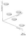
- FIG. 1 a graph is provided showing prior art instruments.
- the graph shows where various existing test instruments fall within a market space defined by performance, density, and cost.
- instrument A offers high performance, but at a high cost and low density.
- Instrument B provides low cost, but suffers from low performance and low density.
- Instrument C offers high density; however, instrument C has an associated high cost and low performance. None of the instruments offers high performance, high density, and low cost, and none of them is reconfigurable to occupy different positions in the performance-density-cost space.
- a testing architecture includes a signal generation core coupled to a plurality of channels.
- the signal generation core is configurable to provide a cancellation signal to one or more of the channels, wherein respective channels can selectively apply the cancellation signal to improve their accuracy.
- respective channels can selectively apply the cancellation signal to improve their accuracy.
- different combinations of performance, density, and overall cost can be achieved.
- FIG. 2 shows an illustrative embodiment of the invention.
- an architecture 10 includes a high precision signal source 11 coupled to multiple channels, generally 12a - 12n. Although three channels are shown, it should be understood that any number of channels can be provided.
- the high precision source 11 is connected to the channels via switches 201 and 204. These switches, which are preferably form-C relays, can alternatively connect the high precision source 11 to the channels 12a - 12n via external adjust 80.
- External adjust 80 is an optional, user-specified circuit than can be used vary the characteristics of the signal produced by the high precision source, in ways that are tailored to a customer's particular application. In alternative embodiments, external adjust 80 can be omitted.
- Each channel 12a - 12n has a source portion and a capture portion.
- the source portion includes a DAC 91, which is used to provide signals to a device under test.
- a switch 212 such as a form-C relay, connects a signal provided by the output of DAC 91 to the device under test. In particular, with the relay 212 in the "down" position, its output signal is conveyed to the output of the respective channel at node 152.
- the source portion preferably includes other circuitry, such as an output amplifier, but this circuitry is omitted for clarity of illustration.
- the capture portion of the channel 12 includes a combiner 143, which receives a signal under test (SUT) at node 150 from a device under test. With the relay 212 in its "up" position, combiner 143 also receives a DC baseline signal at another input, from DAC 91. The output of combiner 143 is provided to an input of combiner 142. Combiner 142 also receives a cancellation signal from the source 11 via an amplifier 161 and a switch 209. The output of combiner 142 is provided to an amplifier 160. The output of the amplifier 160 is provided to an ADC 130.
- the combiners 142 and 143 are preferably analog adding circuits.
- the tester In ATE systems, the tester generally controls both the application of stimuli and the measurement of responses. Often, stimuli are processed by devices under test before being returned to the tester for measurement. Because the tester controls both stimuli and responses, responses generally have expected characteristics (e.g., frequency, amplitude, DC offset, phase) that either match those of the stimuli or deviate therefrom in predictable ways, based on expected behavior of the device under test. Consequently, captured signals usually have known, or at least expected, characteristics.
- expected characteristics e.g., frequency, amplitude, DC offset, phase
- the architecture 10 is configurable in different capture modes.
- the high precision source produces an AC cancellation signal that preferably equals the AC component of the expected SUT.
- the AC cancellation signal has substantially no DC component.
- the DAC 91 produces a DC baseline signal that preferably equals the DC component of the expected SUT.
- the DC baseline signal preferably has substantially no AC component.
- the combiner 143 subtracts the DC component of the SUT, and the combiner 142 subtracts the AC component of the SUT. Assuming no noise, distortion, or other error in the SUT, the output of the combiner 142 should ideally be zero.
- the output signal from the combiner 142 has a small, yet non-zero value.
- This signal is boosted by amplifier 160, which preferably has programmable gain, to a level that can be accurately measured by the ADC 130. A precise reading of the errors in the SUT can then be determined.
- the DAC 91 preferably performs two functions. When the channel 12 is used as a source, the DAC 91 provides an output signal at node 152. When the channel 12 is used as a capture, the DAC 91 provides a DC baseline signal that is used for canceling any DC component on a signal applied at node 150.
- the above described architecture 10 can be used in different modes to provide various signal capture characteristics, depending upon the demands of the test to be performed.
- the architecture is used in thee modes, which are configurable by way of the relays 209 and 212.
- the relays are preferably controlled by an instrument driver, which controls the architecture 10.
- a first mode (i.e., "mode 1"), provides a low-cost, high-density test configuration. Mode 1 operates without signal cancellation; therefore, the signal generation core is not required. In mode 1, all the channels are configured the same way. Relays 212 are preferably in the "up” position, and relays 209 are preferably in the "down” position. These configurations allow the DC component of the SUT to be reduced, prior to measurement (via DC baseline from the DAC 91), but do not allow for reduction of the AC component of the SUT.
- a SUT from the device under test is applied to node 150. Because relay 212 is in the "up" position, Combiner 143 subtracts the DC baseline from the SUT. The output of combiner 143 is provided to combiner 142. Relay 209 is configured to disconnect the AC cancellation signal from combiner 142. The output of combiner 142 is fed to signal amplifier 160, without AC cancellation, and the output of signal amplifier 160 is coupled to ADC 130. In such a manner a signal from the device under test is received.
- a similar configuration may be used with channels 12b-12n in this mode. Because this mode provides high density signal capture at low cost per channel, this mode is especially suitable for multi-site testing or other forms of testing where multiple, simultaneous captures are needed.
- a second mode can be used to provide high performance and low density.
- mode 2 all channels 12a - 12n except one are configured similarly to channels 12a- 12n in mode 1.
- one channel for example, channel 12n, is configured to apply signal cancellation.
- relay 209 is switched to the "up" position for channel 12n only.
- a cancellation signal is provided by source 11, through relays 201 and 204 to channel 12n.
- the signal from source 11 is provide to amplifier 161.
- the output of amplifier 161 is provided through relay 209 to combiner 142.
- the signal from the device under test is received at node 150, and passed to the combiner 143.
- DC cancellation is applied by the combiner 143 (via subtraction of the DC baseline).
- combiner 143 The output of combiner 143 is provided to combiner 142.
- Combiner 142 combines the cancellation signal from amplifier 161 with the received signal to produce a difference signal, the difference signal representing the difference between the received signal and the cancellation signal from the high precision source. This difference signal is coupled to amplifier 160 to produce a residual signal. The residual signal is then provided to ADC 130. This residual signal is corrected for both DC and AC components, and should ideally be zero, except to the extent that errors are present.
- the architecture 10 can be configured in a third mode.
- this mode i.e., "mode 3”
- a parallel mixed capture with and without signal cancellation is provided.
- Mode 3 thus provides moderate performance and high density.
- all the channels 12a - 12nare configured to provide a signal capture using both AC and DC signal cancellation. These channels are configured in a similar fashion as channel 12n of mode 2.
- mode 3 achieves significant accuracy improvement over mode 1 though the use of a cancellation signal that is approximately correct.
- testing should be arranged so that a common AC cancellation signal can be used, with reasonable accuracy, for all channels.
- the cancellation signal may be selected, for example, to be a best fit for all the channels, such as a median of ideal cancellation signals for all the channels being used.
- This mode thus has favorable applications to multi-site testing. In multi-site testing, different, nominally identical devices are tested simultaneously in parallel using nominally identical stimuli. These stimuli produce nominally identical responses (SUTs), which can be tested at high density, relatively high performance, and at relatively low cost per channel.
- SUTs nominally identical responses
- the input to the amplifier 160 need not approach zero for a channel to realize significant improvements in capture accuracy. For example, reducing the amplitude of the signal input to the amplifier 160 by a factor of ten affords a 20dB improvement for that channel, which is otherwise difficult to achieve.
- each channel can individually provide a different DC cancellation signal (i.e., DC baseline) by appropriately programming the respective DAC 91.
- Each of the channels 12a - 12n preferably is provided at much lower cost than that of the high precision source 11.
- the high accuracy of these channels is attainable through the application of the cancellation signal from the high precision source.
- the cost of the high precision source is thus distributed over the number of channels to reduce the overall cost per channel.
- amplifiers 160 and 161 have programmable gain.
- the gain of amplifier 160 is preferably variable to produce a large signal for input to the ADC 130.
- ADC's produce more accurate readings when converting larger signals than when converting smaller signals, because larger signals are less affected by quantization errors of the ADC and noise. Varying the gain of amplifier 160 thus enables the ADC to perform at its best.
- the gain of amplifier 161 is preferably variable to maximize the effectiveness of AC signal cancellation.
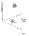
- FIG. 3 a graph, similar to the graph of Figure 1, is shown.
- This graph shows how the same tester, configurable into multiple modes, meets different criteria relating to performance, cost and density.
- a low cost, high-density instrument is provided.
- a high precision and low density tester is achieved.
- mode 3 a moderate precision, high-density tester is configured.
- the present test system can be configured into multiple modes, and to provide multiple functions at different cost, density and performance levels.
- the embodiment disclosed herein includes channels that provide both source and capture functions.
- the channels can provide capture function only.
- the DAC 91 provides a DC baseline to separately cancel DC offsets in the SUT on a per channel basis.
- a single DC source could be provided to adjust the DC baseline for all channels together.
- a DC source could be incorporated into the high precision source 11, which would then correct both AC and DC components of the SUTs. Note that this configuration would not be preferred, however, because cancellation on a per channel basis is more flexible than a single cancellation for all channels.
- the foregoing description prescribes three distinct modes of operation for the architecture 10. It should be understood, however, that these modes are not necessarily mutually exclusive. For instance, certain channels can be operated in mode 1 (without AC cancellation) while one or more other channels are simultaneously operated in mode 2 (with precise AC cancellation). Other channels can simultaneously be operated in mode 3 (with approximate AC cancellation), by applying the same cancellation signal that is used for the channels running in mode 2. Therefore, different channels of the architecture can be operated in different modes, simultaneously.
- Additional flexibility can be achieved, although at additional cost, by providing one or more additional high precision sources 11, to which channels can selectively connect.
- the economic advantages of the invention are preserved, despite the additional cost, as long as the number of channels significantly exceeds the number of high precision sources.
- Each channel can be allocated to one particular high precision source, or channels can be switchably connectable to different sources for greater flexibility.
Landscapes
- Engineering & Computer Science (AREA)
- General Engineering & Computer Science (AREA)
- Computer Hardware Design (AREA)
- Microelectronics & Electronic Packaging (AREA)
- Physics & Mathematics (AREA)
- General Physics & Mathematics (AREA)
- Tests Of Electronic Circuits (AREA)
- Amplifiers (AREA)
- Analogue/Digital Conversion (AREA)
Applications Claiming Priority (2)
| Application Number | Priority Date | Filing Date | Title |
|---|---|---|---|
| US749704 | 2003-12-31 | ||
| US10/749,704 US7230553B2 (en) | 2003-12-31 | 2003-12-31 | Parallel source/capture architecture |
Publications (1)
| Publication Number | Publication Date |
|---|---|
| EP1550878A1 true EP1550878A1 (de) | 2005-07-06 |
Family
ID=34574794
Family Applications (1)
| Application Number | Title | Priority Date | Filing Date |
|---|---|---|---|
| EP04030707A Withdrawn EP1550878A1 (de) | 2003-12-31 | 2004-12-23 | Parallele Quellen- und Erfassungsarchitektur für automatische Testsysteme |
Country Status (6)
| Country | Link |
|---|---|
| US (1) | US7230553B2 (de) |
| EP (1) | EP1550878A1 (de) |
| JP (1) | JP4392342B2 (de) |
| CN (1) | CN100529782C (de) |
| SG (1) | SG113007A1 (de) |
| TW (1) | TWI272400B (de) |
Families Citing this family (5)
| Publication number | Priority date | Publication date | Assignee | Title |
|---|---|---|---|---|
| US20090237209A1 (en) * | 2008-03-20 | 2009-09-24 | Brian William Seal | Communicating keychain |
| US7969171B1 (en) * | 2010-01-06 | 2011-06-28 | General Electric Company | Test circuit and system |
| US11586883B2 (en) * | 2018-12-14 | 2023-02-21 | Microsoft Technology Licensing, Llc | Residual quantization for neural networks |
| CN115812142B (zh) | 2020-06-12 | 2026-04-21 | 亚德诺半导体国际无限责任公司 | 自校准聚合物纳米复合物(pnc)传感元件 |
| DE112021005751T5 (de) * | 2020-10-27 | 2023-08-17 | Analog Devices, Inc. | Drahtlosintegritätserfassungsbeschaffungsmodul |
Citations (4)
| Publication number | Priority date | Publication date | Assignee | Title |
|---|---|---|---|---|
| US4189778A (en) * | 1977-10-31 | 1980-02-19 | Uriel Vogel | Method and instrumentation for the measurement of parameters of system devices |
| JPS58200170A (ja) * | 1982-05-17 | 1983-11-21 | Oki Electric Ind Co Ltd | 消費電流測定回路 |
| JP2001281303A (ja) * | 2000-03-28 | 2001-10-10 | Yamaha Corp | 半導体集積回路試験装置、半導体集積回路試験装置の校正方法及び記録媒体 |
| US6449741B1 (en) * | 1998-10-30 | 2002-09-10 | Ltx Corporation | Single platform electronic tester |
Family Cites Families (10)
| Publication number | Priority date | Publication date | Assignee | Title |
|---|---|---|---|---|
| US5659312A (en) * | 1996-06-14 | 1997-08-19 | Logicvision, Inc. | Method and apparatus for testing digital to analog and analog to digital converters |
| US6449568B1 (en) * | 1998-02-27 | 2002-09-10 | Eni Technology, Inc. | Voltage-current sensor with high matching directivity |
| US6271781B1 (en) * | 1998-06-10 | 2001-08-07 | Lockheed Martin Corporation | Nonlinear filter correction of multibit ΣΔ modulators |
| JP2002296329A (ja) * | 2001-03-30 | 2002-10-09 | Agilent Technologies Japan Ltd | 集積回路の試験装置 |
| US6667702B2 (en) * | 2001-04-27 | 2003-12-23 | Rohm Co., Ltd | Semiconductor device having DACs and method of testing such semiconductor device |
| US6700514B2 (en) * | 2002-03-14 | 2004-03-02 | Nec Corporation | Feed-forward DC-offset canceller for direct conversion receiver |
| US6642874B1 (en) * | 2002-10-11 | 2003-11-04 | Realtek Semiconductor Corp. | Sigma-delta data conversion employing quantization error feedback |
| WO2005018134A2 (en) * | 2003-08-07 | 2005-02-24 | Quellan, Inc. | Method and system for crosstalk cancellation |
| US6919833B2 (en) * | 2003-09-04 | 2005-07-19 | Regan N. Mills | Parallel converter topology for reducing non-linearity errors |
| US7265694B2 (en) * | 2004-03-25 | 2007-09-04 | Texas Instruments Incorporated | System and method for successive approximation |
-
2003
- 2003-12-31 US US10/749,704 patent/US7230553B2/en not_active Expired - Lifetime
-
2004
- 2004-12-21 TW TW093139806A patent/TWI272400B/zh not_active IP Right Cessation
- 2004-12-22 SG SG200407645A patent/SG113007A1/en unknown
- 2004-12-23 EP EP04030707A patent/EP1550878A1/de not_active Withdrawn
- 2004-12-28 JP JP2004379858A patent/JP4392342B2/ja not_active Expired - Lifetime
- 2004-12-30 CN CNB2004101049045A patent/CN100529782C/zh not_active Expired - Lifetime
Patent Citations (4)
| Publication number | Priority date | Publication date | Assignee | Title |
|---|---|---|---|---|
| US4189778A (en) * | 1977-10-31 | 1980-02-19 | Uriel Vogel | Method and instrumentation for the measurement of parameters of system devices |
| JPS58200170A (ja) * | 1982-05-17 | 1983-11-21 | Oki Electric Ind Co Ltd | 消費電流測定回路 |
| US6449741B1 (en) * | 1998-10-30 | 2002-09-10 | Ltx Corporation | Single platform electronic tester |
| JP2001281303A (ja) * | 2000-03-28 | 2001-10-10 | Yamaha Corp | 半導体集積回路試験装置、半導体集積回路試験装置の校正方法及び記録媒体 |
Non-Patent Citations (2)
| Title |
|---|
| PATENT ABSTRACTS OF JAPAN vol. 008, no. 048 (P - 258) 3 March 1984 (1984-03-03) * |
| PATENT ABSTRACTS OF JAPAN vol. 2002, no. 02 2 April 2002 (2002-04-02) * |
Also Published As
| Publication number | Publication date |
|---|---|
| CN100529782C (zh) | 2009-08-19 |
| CN1797020A (zh) | 2006-07-05 |
| SG113007A1 (en) | 2005-07-28 |
| TW200535438A (en) | 2005-11-01 |
| JP4392342B2 (ja) | 2009-12-24 |
| US20050149807A1 (en) | 2005-07-07 |
| US7230553B2 (en) | 2007-06-12 |
| JP2005195592A (ja) | 2005-07-21 |
| TWI272400B (en) | 2007-02-01 |
Similar Documents
| Publication | Publication Date | Title |
|---|---|---|
| US6066953A (en) | Architecture for RF signal automatic test equipment | |
| US6768349B2 (en) | Multiple-output arbitrary waveform generator and mixed lsi tester | |
| US8078130B2 (en) | Systems and methods for interference cancellation | |
| US8081946B2 (en) | Interference cancellation for reconfigurable direct RF bandpass sampling interference cancellation | |
| JP3909102B2 (ja) | Rf電力測定装置 | |
| US6900750B1 (en) | Signal conditioning system with adjustable gain and offset mismatches | |
| US20040121746A1 (en) | Direct conversion receiver | |
| EP1149474A1 (de) | Kalibrierung und kompensation von delta-sigma adc's und dac's mittels korrelierung von rauschsignalen | |
| US7230553B2 (en) | Parallel source/capture architecture | |
| US7049989B2 (en) | Unified analog input front end apparatus and method | |
| US20040177293A1 (en) | Programmable multi-function module for automatic test equipment systems | |
| EP4667949A2 (de) | Breitband-spektralanalysator | |
| US20070268012A1 (en) | Waveform input circuit, waveform observation unit and semiconductor test apparatus | |
| US6756807B2 (en) | Modular ATE power supply architecture | |
| US7236116B2 (en) | Reconfigurable switched-capacitor input circuit with digital-stimulus acceptability for analog tests | |
| US11411662B2 (en) | Calibration system | |
| US8354834B2 (en) | Methods and apparatus for acquiring measurements and performing an auto-zero process using a multi-range measurement apparatus | |
| CN113125989B (zh) | Dc电源轨探头和测量方法 | |
| WO2011020479A1 (en) | Optimized automated test equipment multi-path receiver concept | |
| US12385959B2 (en) | Method and system for component mismatch compensation | |
| US20250150088A1 (en) | System and methods for configurable input channel multiplexing | |
| JP4822682B2 (ja) | イコライザ回路、高周波アナログ信号伝送路並びにハードディスクの検査装置 | |
| CN210604778U (zh) | 一种频率特性分析仪 | |
| JP4207107B2 (ja) | Icテスタ | |
| WO2025101218A1 (en) | System and methods for configurable input channel multiplexing |
Legal Events
| Date | Code | Title | Description |
|---|---|---|---|
| PUAI | Public reference made under article 153(3) epc to a published international application that has entered the european phase |
Free format text: ORIGINAL CODE: 0009012 |
|
| AK | Designated contracting states |
Kind code of ref document: A1 Designated state(s): AT BE BG CH CY CZ DE DK EE ES FI FR GB GR HU IE IS IT LI LT LU MC NL PL PT RO SE SI SK TR |
|
| AX | Request for extension of the european patent |
Extension state: AL BA HR LV MK YU |
|
| 17P | Request for examination filed |
Effective date: 20051228 |
|
| AKX | Designation fees paid |
Designated state(s): DE FR GB IE IT |
|
| GRAP | Despatch of communication of intention to grant a patent |
Free format text: ORIGINAL CODE: EPIDOSNIGR1 |
|
| STAA | Information on the status of an ep patent application or granted ep patent |
Free format text: STATUS: THE APPLICATION IS DEEMED TO BE WITHDRAWN |
|
| 18D | Application deemed to be withdrawn |
Effective date: 20080401 |