EP1549464B1 - Retaining ring for holding semiconductor wafers in a chemical-mechanical polishing device - Google Patents
Retaining ring for holding semiconductor wafers in a chemical-mechanical polishing device Download PDFInfo
- Publication number
- EP1549464B1 EP1549464B1 EP03779799A EP03779799A EP1549464B1 EP 1549464 B1 EP1549464 B1 EP 1549464B1 EP 03779799 A EP03779799 A EP 03779799A EP 03779799 A EP03779799 A EP 03779799A EP 1549464 B1 EP1549464 B1 EP 1549464B1
- Authority
- EP
- European Patent Office
- Prior art keywords
- retaining ring
- plastics material
- ring
- metal ring
- ring according
- Prior art date
- Legal status (The legal status is an assumption and is not a legal conclusion. Google has not performed a legal analysis and makes no representation as to the accuracy of the status listed.)
- Expired - Lifetime
Links
- 238000005498 polishing Methods 0.000 title claims abstract description 40
- 235000012431 wafers Nutrition 0.000 title claims abstract description 18
- 239000004065 semiconductor Substances 0.000 title claims abstract description 12
- 239000004033 plastic Substances 0.000 claims abstract description 41
- 229920003023 plastic Polymers 0.000 claims abstract description 41
- 239000000463 material Substances 0.000 claims abstract description 38
- 239000000126 substance Substances 0.000 claims abstract description 6
- 239000002184 metal Substances 0.000 claims description 37
- 229910052751 metal Inorganic materials 0.000 claims description 37
- 229920002430 Fibre-reinforced plastic Polymers 0.000 claims description 2
- 239000000654 additive Substances 0.000 claims description 2
- 229920001971 elastomer Polymers 0.000 claims description 2
- 239000000806 elastomer Substances 0.000 claims description 2
- 239000011151 fibre-reinforced plastic Substances 0.000 claims description 2
- 239000000203 mixture Substances 0.000 claims description 2
- 229920001169 thermoplastic Polymers 0.000 claims description 2
- 239000004416 thermosoftening plastic Substances 0.000 claims description 2
- 239000002990 reinforced plastic Substances 0.000 claims 1
- 230000002787 reinforcement Effects 0.000 claims 1
- 230000000717 retained effect Effects 0.000 claims 1
- 229920001187 thermosetting polymer Polymers 0.000 claims 1
- 239000000758 substrate Substances 0.000 description 10
- 238000004519 manufacturing process Methods 0.000 description 5
- 238000000034 method Methods 0.000 description 5
- 239000000853 adhesive Substances 0.000 description 3
- 230000001070 adhesive effect Effects 0.000 description 3
- 239000003795 chemical substances by application Substances 0.000 description 3
- 239000007769 metal material Substances 0.000 description 3
- 238000007517 polishing process Methods 0.000 description 3
- 239000012779 reinforcing material Substances 0.000 description 3
- 238000005299 abrasion Methods 0.000 description 2
- 239000013043 chemical agent Substances 0.000 description 2
- 229920006332 epoxy adhesive Polymers 0.000 description 2
- 230000003014 reinforcing effect Effects 0.000 description 2
- 239000000243 solution Substances 0.000 description 2
- 229910052582 BN Inorganic materials 0.000 description 1
- PZNSFCLAULLKQX-UHFFFAOYSA-N Boron nitride Chemical compound N#B PZNSFCLAULLKQX-UHFFFAOYSA-N 0.000 description 1
- OKTJSMMVPCPJKN-UHFFFAOYSA-N Carbon Chemical compound [C] OKTJSMMVPCPJKN-UHFFFAOYSA-N 0.000 description 1
- 239000004642 Polyimide Substances 0.000 description 1
- XUIMIQQOPSSXEZ-UHFFFAOYSA-N Silicon Chemical compound [Si] XUIMIQQOPSSXEZ-UHFFFAOYSA-N 0.000 description 1
- 238000004873 anchoring Methods 0.000 description 1
- 230000015556 catabolic process Effects 0.000 description 1
- 230000000295 complement effect Effects 0.000 description 1
- 150000001875 compounds Chemical class 0.000 description 1
- 238000005260 corrosion Methods 0.000 description 1
- 230000007797 corrosion Effects 0.000 description 1
- 238000006731 degradation reaction Methods 0.000 description 1
- 238000000151 deposition Methods 0.000 description 1
- 230000000694 effects Effects 0.000 description 1
- 238000005538 encapsulation Methods 0.000 description 1
- 229910002804 graphite Inorganic materials 0.000 description 1
- 239000010439 graphite Substances 0.000 description 1
- 238000010438 heat treatment Methods 0.000 description 1
- 238000002347 injection Methods 0.000 description 1
- 239000007924 injection Substances 0.000 description 1
- CWQXQMHSOZUFJS-UHFFFAOYSA-N molybdenum disulfide Chemical compound S=[Mo]=S CWQXQMHSOZUFJS-UHFFFAOYSA-N 0.000 description 1
- 229910052982 molybdenum disulfide Inorganic materials 0.000 description 1
- 239000002105 nanoparticle Substances 0.000 description 1
- 239000002245 particle Substances 0.000 description 1
- 230000002093 peripheral effect Effects 0.000 description 1
- 229920001721 polyimide Polymers 0.000 description 1
- 239000004810 polytetrafluoroethylene Substances 0.000 description 1
- 229920001343 polytetrafluoroethylene Polymers 0.000 description 1
- 239000004576 sand Substances 0.000 description 1
- 229910052710 silicon Inorganic materials 0.000 description 1
- 239000010703 silicon Substances 0.000 description 1
- 238000007669 thermal treatment Methods 0.000 description 1
Images

Classifications
-
- H—ELECTRICITY
- H01—ELECTRIC ELEMENTS
- H01L—SEMICONDUCTOR DEVICES NOT COVERED BY CLASS H10
- H01L21/00—Processes or apparatus adapted for the manufacture or treatment of semiconductor or solid state devices or of parts thereof
- H01L21/02—Manufacture or treatment of semiconductor devices or of parts thereof
- H01L21/04—Manufacture or treatment of semiconductor devices or of parts thereof the devices having at least one potential-jump barrier or surface barrier, e.g. PN junction, depletion layer or carrier concentration layer
- H01L21/18—Manufacture or treatment of semiconductor devices or of parts thereof the devices having at least one potential-jump barrier or surface barrier, e.g. PN junction, depletion layer or carrier concentration layer the devices having semiconductor bodies comprising elements of Group IV of the Periodic System or AIIIBV compounds with or without impurities, e.g. doping materials
- H01L21/30—Treatment of semiconductor bodies using processes or apparatus not provided for in groups H01L21/20 - H01L21/26
- H01L21/302—Treatment of semiconductor bodies using processes or apparatus not provided for in groups H01L21/20 - H01L21/26 to change their surface-physical characteristics or shape, e.g. etching, polishing, cutting
- H01L21/304—Mechanical treatment, e.g. grinding, polishing, cutting
-
- B—PERFORMING OPERATIONS; TRANSPORTING
- B24—GRINDING; POLISHING
- B24B—MACHINES, DEVICES, OR PROCESSES FOR GRINDING OR POLISHING; DRESSING OR CONDITIONING OF ABRADING SURFACES; FEEDING OF GRINDING, POLISHING, OR LAPPING AGENTS
- B24B37/00—Lapping machines or devices; Accessories
- B24B37/27—Work carriers
- B24B37/30—Work carriers for single side lapping of plane surfaces
- B24B37/32—Retaining rings
Definitions
- the invention relates to a retaining ring for holding semiconductor wafers in a chemical-mechanical polishing apparatus according to the preamble of claim 1.
- CMP chemical mechanical polishing
- a recurring problem in the CMP process is the so-called edge effect, i. the tendency to polish the edge of the substrate to be polished at a different speed than the center of the substrate. This typically results in too much polishing at the edge, i. Here too much material is removed from the edge, especially at the outermost 5 to 10 mm of a wafer of 200 mm in diameter.
- US Pat. No. 6,251,215 proposes to make the retaining ring in two parts, wherein one part is made of a rigid material, namely a metal part, and a second part of a plastic material, which has a lower rigidity, so that on the one hand, it can be subjected to abrasive loading and, on the other hand, it can not damage it in contact with the semiconductor wafer.
- U.S. Patent No. 6,251,215 suggests bonding the plastic part of the retaining ring and the metal ring together with an epoxy adhesive. Alternatively, it is proposed to connect the two parts in an interference fit with each other.
- the processing of the retaining ring after a certain abrasion of the plastic part causes problems.
- the complete retaining rings must be returned to the manufacturer, where the plastic part is mechanically removed and subsequently the adhesive residues from the metal part are thermally decomposed by heating to about 200 ° C. Thereafter, the metal part must be sandblasted to remove the last remnants of the adhesive, and only then can a new plastic ring be glued on again.
- the retaining rings are very expensive as such.
- the metallic holding elements which are more expensive than the plastic elements from the production costs, survive only a small number of cycles, in particular because of the thermal treatment during thermal degradation of the adhesive and the subsequently required sand blast treatment.
- Object of the present invention is to propose a retaining ring which avoids the above problems.
- the inventive design of the retaining ring allows cost-effective production, so that after excessive wear of the retaining ring can be thrown away as a whole.
- the plastic material is selected according to its mechanical properties.
- the retaining ring is composed of at least two layers or components sandwiched.
- the plastic material may comprise, for example, a thermoplastic, a duroplastic, an elastomer and / or a plastic mixture.
- the plastic material adjacent to its first end i. the side which forms the support surface for supporting the retaining ring on a polishing surface of the polishing device, without reinforcing materials or with a lower content of reinforcing materials than on its side comprising the mounting elements.
- the retaining ring has lower strengths and in particular is less hard, so that contact between the machined Semiconductor wafers and the plastic material for the wafer is gentle.
- the plastic material friction and / or wear-reducing additives may be mixed, for example, PTFE, polyimide, molybdenum disulfide, graphite, boron nitride, nanoparticles or the like.
- the reinforcing materials are limited to a core region of the retaining ring, in particular the region in which then the mounting elements are arranged. This gives the retaining ring the necessary rigidity and geometric integrity even with one-sided loads, while a contact of the retaining ring with the wafer can not lead to damage of the wafer, since the wafer comes into contact only with the softer plastic materials.
- the retaining ring comprises a cast in the plastic material metal ring, which is arranged concentrically in the retaining ring.
- the metal ring provides the necessary rigidity and geometric integrity of the retaining ring, while in turn the surrounding plastic material ensures that the semiconductor wafer to be processed is not subjected to any mechanical damage.
- the mounting elements will then be held on the metal ring, so that these, which indeed serve to mount the retaining ring on the polishing device, ensure an exact contact of the retaining ring on the polishing device and thus additionally secure the geometric structure of the retaining ring.
- the metal ring which is surrounded by the plastic material, can remain uncovered, in particular on the upper side, ie on the side of the retaining ring, which faces the polishing apparatus, since there is no contact with the wafer material get hold of. Likewise, this side of the retaining ring is little or not exposed to the chemical agents of the chemical-mechanical polishing process.
- the simplest form for the metal ring for reinforcing the retaining ring is a sheet metal ring. This can in particular be perforated or generally provided with openings, so that a positive connection between the plastic material and the metal ring takes place through the plastic material passing through the openings.
- a sheet metal ring having a substantially cylindrical shape is preferred. used in the form of a cylinder wall.
- metal washers may be used, in which case a greater thickness of the sheet material may be required.
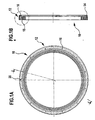
- Figures 1A to 1D show a retaining ring 10 according to the invention, which is made of a fiber-reinforced plastic material and having a substantially rectangular cross-section.
- the retaining ring 10 Adjacent to the outer circumference 12, the retaining ring 10 has an axially projecting circumferential collar 14, in which threaded bushes 16 are inserted at regular angular intervals.
- the threaded bushes 16 are used for fastening the retaining ring in the chemical-mechanical polishing apparatus.
- the collar 14 opposite side of the retaining ring 10 forms a bearing surface 18 with which the retaining ring 10 rests during operation of the polishing device on a polishing surface thereof.
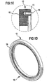
- FIG. 1B shows the retaining ring 10 according to the invention along the section line A-A in FIG. 1A.
- FIG. 1C shows an enlarged detail from the sectional view of FIG. 1B.
- FIG. 1D the retaining ring 10 according to the invention is again shown in a perspective view.
- the circumferential collar 14 has on its pointing to the polishing device surface on a recess 20 in which engages in the assembled state by the polishing a complementary projection to facilitate the correct angular orientation of the retaining ring 10 relative to the polishing device, so that an alignment of the threaded bushing 16 with corresponding breakthroughs on the part of the polishing device, protrude through the bolts, can be achieved automatically.
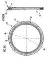
- FIG. 2A to 2D A further embodiment is shown in Figures 2A to 2D in the form of a retaining ring 30.
- the structure of the retaining ring 30 differs from the structure of the retaining ring 10 in particular in that here as a reinforcing element for the plastic material in this a metal ring 32 is embedded.
- the metal ring is arranged concentrically to the retaining ring 30 and made of a perforated sheet material.
- the plastic material will pass through the apertures of the perforated material during encapsulation of the metal ring 32 and thus lead to a positive anchoring of the metal ring 32 in the retaining ring 30.
- the retaining ring 30 further has, on its side facing the polishing device on an axially projecting collar 34, which is adjacent to the outer peripheral surface 36 of the retaining ring 30 is disposed.
- an axially projecting collar 34 which is adjacent to the outer peripheral surface 36 of the retaining ring 30 is disposed.
- threaded bushes 40 are arranged at regular angular intervals, by means of which the retaining ring 30 can be mounted in the polishing device.
- the collar 34 has a recess 42, which engages in the part of the polishing device, a projection and thus ensures an angularly correct mounting of the retaining ring 30.
- the plastic material may be selected from a wider range and, in particular, optimized for the abrasion resistance requirements of the polishing surface of the polishing apparatus.
- the rigidity of the retaining ring 30 is ensured here essentially by the strength and geometric integrity of the metal ring 32 (annular disc).
- the metal ring 32 can serve to carry the threaded bushes 40, so that the metal ring 32 can be prefabricated with the threaded bushes 40, inserted into an injection mold and then encapsulated with plastic. Due to the fact that the metal ring 32 is substantially completely surrounded by the plastic material of the retaining ring 30, the metallic material from which the metal ring 32 is made, can also be selected from a wide range of materials, since this hardly or not at all the chemical agents used for the chemical-mechanical polishing of the semiconductor wafers comes into contact. Corrosion problems are therefore not to be expected.
Abstract
Description
Die Erfindung betrifft einen Haltering zum Halten von Halbleiterwafern in einer chemisch-mechanischen Poliervorrichtung nach dem Oberbegriff des Anspruchs 1.The invention relates to a retaining ring for holding semiconductor wafers in a chemical-mechanical polishing apparatus according to the preamble of
Heutzutage werden integrierte Schaltkreise typischerweise auf Halbleitersubstraten, insbesondere Siliziumwafern, hergestellt, wobei nacheinander leitende, halbleitende und isolierende Schichten auf dem Wafer abgeschieden werden. Nachdem jede Schicht abgelagert ist, wird geätzt, um die Schaltkreisfunktionen zu realisieren. Nachdem eine Reihe von Lagen sequenziell gelagert und geätzt wurde, wird die oberste Oberfläche des Halbleitersubstrates, d.h. die außenliegende Oberfläche des Substrates, mehr und mehr uneben. Diese unebene Oberfläche bereitet in photolitographischen Schritten beim Herstellungsprozess der integrierten Schaltkreise Probleme. Deshalb besteht die Notwendigkeit immer wieder, die Oberfläche des Malbfeitersubsfirates plan zu machen bzw. einzuebnen.Today, integrated circuits are typically fabricated on semiconductor substrates, particularly silicon wafers, sequentially depositing conductive, semiconductive, and insulating layers onto the wafer. After each layer is deposited, it is etched to realize the circuit functions. After a series of layers have been sequentially stored and etched, the top surface of the semiconductor substrate, i. the outer surface of the substrate, more and more uneven. This uneven surface causes problems in photolithographic steps in the integrated circuit manufacturing process. Therefore, there is a need again and again to make the surface of the Malbfeitersubsfirates plan or level.
Hierfür stellt das sogenannte chemisch-mechanische Polieren (CMP) eine der anerkannten Methoden dar. Dieses Verfahren zur Erzielung der Planheit verlangt typischerweise, dass das Substrat, d.h. der Halbleiterwafer, auf einem Träger oder auch Polierkopf montiert wird. Die freiliegende Oberfläche des Substrates wird dann gegen eine rotierende Polierscheibe gedrückt. Über den Trägerkopf wird eine geregelte Kraft auf das Substrat ausgeübt, um dieses gegen die Polierscheibe zu drücken. Ein Poliermittel, welches mindestens ein chemisch reaktives Agens und abrasive Partikel enthält, wird auf die Oberfläche der Polierscheibe gegeben.For this purpose, the so-called chemical mechanical polishing (CMP) is one of the recognized methods. This method of obtaining the flatness typically requires that the substrate, ie the semiconductor wafer, be mounted on a carrier or polishing head. The exposed surface of the substrate is then pressed against a rotating polishing pad. A controlled force is applied to the substrate via the carrier head in order to press it against the polishing pad. A polishing agent containing at least one chemically reactive agent and abrasive particles is placed on the surface of the polishing pad.
Ein immer wiederkehrendes Problem in dem CMP-Verfahren ist der sogenannte Randeffekt, d.h. die Tendenz, den Rand des Substrates, welches zu polieren ist, mit einer anderen Geschwindigkeit als die Mitte des Substrates zu polieren. Daraus resultiert typischerweise ein Zuviel an Polieren am Rand, d.h. hier wird zuviel Material vom Rand abgetragen, insbesondere bei den äußersten 5 bis 10 mm eines Wafers von 200 mm im Durchmesser.A recurring problem in the CMP process is the so-called edge effect, i. the tendency to polish the edge of the substrate to be polished at a different speed than the center of the substrate. This typically results in too much polishing at the edge, i. Here too much material is removed from the edge, especially at the outermost 5 to 10 mm of a wafer of 200 mm in diameter.
Das Zuviel an Polieren reduziert die Ebenheit des Substrates über das Gesamte gesehen und macht den Rand des Substrates ungeeignet für die Herstellung von integrierten Schaltkreisen und verringert somit die Prozessausbeute.Excessive polishing reduces the flatness of the substrate as a whole and renders the edge of the substrate unsuitable for integrated circuit fabrication, thus reducing process yield.
Zur Lösung dieses Problemes schlägt die US-Patentschrift Nr. 6,251,215 vor, den Haltering zweiteilig zu gestalten, wobei ein Teil aus einem steifen Material hergestellt ist, nämlich einem Metallteil, und ein zweiter Teil aus einem Kunststoffmaterial, welches eine geringere Steifigkeit aufweist, so dass es zum Einen abrasiv belastbar ist und zum Anderen in Kontakt mit dem Halbleiterwafer dieses nicht beschädigen kann.To solve this problem, US Pat. No. 6,251,215 proposes to make the retaining ring in two parts, wherein one part is made of a rigid material, namely a metal part, and a second part of a plastic material, which has a lower rigidity, so that on the one hand, it can be subjected to abrasive loading and, on the other hand, it can not damage it in contact with the semiconductor wafer.
Auf Grund der Randbedingungen beim chemisch-mechanischen Polieren schlägt die US-Patentschrift Nr. 6,251,215 vor, den Kunststoffteil des Halteringes und den Metallring mit einem Epoxykleber miteinander zu verbinden. Alternativ wird vorgeschlagen, die beiden Teile im Presssitz miteinander zu verbinden.Due to the constraints of chemical mechanical polishing, U.S. Patent No. 6,251,215 suggests bonding the plastic part of the retaining ring and the metal ring together with an epoxy adhesive. Alternatively, it is proposed to connect the two parts in an interference fit with each other.
In der Praxis erweisen sich beide Lösungen als unzureichend.In practice, both solutions prove to be inadequate.
Während bei der Verbindung der beiden Teile miteinander mittels Epoxykleber das Kunststoffteil sicher an dem Metallteil gehalten wird, bereitet die Aufarbeitung des Halteringes nach einer gewissen Abrasion des Kunststoffteiles Probleme. In der derzeitigen Praxis müssen die kompletten Halteringe an den Hersteller eingeschickt werden, wo das Kunststoffteil mechanisch entfernt wird und nachfolgend die Klebereste von dem Metallteil durch Aufheizen auf ca. 200 °C thermisch zersetzt werden. Danach muss das Metallteil sandgestrahlt werden, um letzte Reste des Klebstoffes zu entfernen, und erst dann kann wieder ein neuer Kunststoffring aufgeklebt werden.While in the connection of the two parts together by means of epoxy adhesive, the plastic part is securely held on the metal part, the processing of the retaining ring after a certain abrasion of the plastic part causes problems. In current practice, the complete retaining rings must be returned to the manufacturer, where the plastic part is mechanically removed and subsequently the adhesive residues from the metal part are thermally decomposed by heating to about 200 ° C. Thereafter, the metal part must be sandblasted to remove the last remnants of the adhesive, and only then can a new plastic ring be glued on again.
Auf Grund dieser zeit- und kostenintensiven Prozedur werden die Halteringe als solche sehr teuer. Hinzu kommt, dass die metallischen Halteelemente, die von den Produktionskosten her teurer sind als die Kunststoffelemente, nur eine geringe Zahl an Zyklen überstehen, insbesondere wegen der Temperaturbehandlung beim thermischen Abbau des Klebstoffes und der nachfolgend notwendigen Sandstrahlbehandlung.Due to this time and cost intensive procedure, the retaining rings are very expensive as such. In addition, the metallic holding elements, which are more expensive than the plastic elements from the production costs, survive only a small number of cycles, in particular because of the thermal treatment during thermal degradation of the adhesive and the subsequently required sand blast treatment.
Einfacher ist der Austausch eines verbrauchten Kunststoffringes bei der Verbindung von Metallteil und Kunststoffteil über einen Presssitz, jedoch stellt sich hier heraus, dass der Presssitz als Verbindung von Kunststoff- und Metallteil ungeeignet ist, um den beim Polierprozess auftretenden Kräften sicher zu widerstehen.It is easier to replace a worn plastic ring in the connection of metal part and plastic part via a press fit, but it turns out here that the press fit as a compound of plastic and metal part is unsuitable to withstand the forces occurring during polishing process safely.
Aus dem US-Patent US 5,695,392 ist unter anderem ein einteiliger Haltering gemäß dem Oberbegriff des Anspruches 1 bekannt.From US Pat. No. 5,695,392, inter alia, a one-piece retaining ring according to the preamble of
Aufgabe der vorliegenden Erfindung ist es, einen Haltering vorzuschlagen, der vorstehend genannte Probleme vermeidet.Object of the present invention is to propose a retaining ring which avoids the above problems.
Diese Aufgabe wird erfindungsgemäß durch den eingangs genannten Haltering gelöst, der die Merkmale des Kennzeichens des Anspruches 1 aufweist.This object is achieved by the above-mentioned retaining ring having the features of the characterizing part of
Die erfindungsgemäße Konstruktion des Halteringes erlaubt eine kostengünstige Fertigung, so dass nach einem übermäßigen Verschleiß der Haltering als Ganzes weggeworfen werden kann.The inventive design of the retaining ring allows cost-effective production, so that after excessive wear of the retaining ring can be thrown away as a whole.
Um bei dem Haltering eine ausreichende Festigkeit zu realisieren, die sicherstellt, dass der Haltering in seiner Geometrie beim Poliervorgang nicht deformiert wird und dadurch zu einem unebenmäßigen Abtrag auf dem Halbleiterwafer führt, wird das Kunststoffmaterial entsprechend seinen mechanischen Eigenschaften ausgewählt.In order to realize sufficient strength in the retaining ring, which ensures that the retaining ring is not deformed in its geometry during the polishing process and thereby leads to an uneven removal on the semiconductor wafer, the plastic material is selected according to its mechanical properties.
Vorzugsweise ist der Haltering aus mindestens zwei Schichten oder Komponenten sandwichartig aufgebaut.Preferably, the retaining ring is composed of at least two layers or components sandwiched.
Das Kunststoffmaterial kann beispielsweise ein Thermoplast, ein Duroplast, ein Elastomer und/oder eine Kunststoffmischung umfassen.The plastic material may comprise, for example, a thermoplastic, a duroplastic, an elastomer and / or a plastic mixture.
Eine wesentlich größere Palette an Kunststoffmaterialen steht dann zur Verfügung, da man das Kunststoffmaterial in verstärkter, insbesondere in faserverstärkter Form einsetzt.A much larger range of plastic materials is then available, since one uses the plastic material in reinforced, especially in fiber-reinforced form.
Hierbei ist vorgesehen, daß das Kunststoffmaterial benachbart zu seiner ersten Stirnseite, d.h. der Seite, die die Auflagefläche zur Auflage des Halteringes auf einer Polieroberfläche der Poliervorrichtung bildet, ohne Verstärkungsstoffe oder mit einem geringeren Gehalt an Verstärkungsstoffen versieht als an seiner die Montageelemente umfassenden Seite.It is provided that the plastic material adjacent to its first end, i. the side which forms the support surface for supporting the retaining ring on a polishing surface of the polishing device, without reinforcing materials or with a lower content of reinforcing materials than on its side comprising the mounting elements.
Dadurch erhält man in dem Bereich, der an der Poliervorrichtung gehalten wird, einen Teilbereich, der eine erhöhte mechanische Stabilität aufweist und der den Haltering in seiner Geometrie insgesamt stabilisiert. Auf der Seite, auf der der abrasive Verschleiß stattfindet, weist dann der Haltering geringere Festigkeiten auf und ist Insbesondere weniger hart, so dass ein Kontakt zwischen den zu bearbeitenden Halbleiterwafern und dem Kunststoffmaterial für die Wafer schonender ist.As a result, in the region which is held on the polishing device, a partial region is obtained which has increased mechanical stability and which stabilizes the retaining ring overall in its geometry. On the side where the abrasive wear takes place, then the retaining ring has lower strengths and in particular is less hard, so that contact between the machined Semiconductor wafers and the plastic material for the wafer is gentle.
Um den Verschleiß zu reduzieren bzw. die tribologischen Eigenschaften zu optimieren, können dem Kunststoffmaterial reib- und/oder verschleißmindernde Zusatzstoffe zugemischt werden, beispielsweise PTFE, Polyimid, Molybdändisulfid, Graphit, Bornitrid, Nanopartikel oder dergleichen.In order to reduce wear or to optimize the tribological properties, the plastic material friction and / or wear-reducing additives may be mixed, for example, PTFE, polyimide, molybdenum disulfide, graphite, boron nitride, nanoparticles or the like.
Vorstellbar ist schließlich auch, dass sich die Verstärkungsstoffe auf einen Kernbereich des Halteringes beschränken, insbesondere den Bereich, in dem dann auch die Montageelemente angeordnet sind. Dies verleiht dem Haltering die notwendige Steifigkeit und geometrische Integrität auch bei einseitigen Belastungen, während ein Kontakt des Halteringes mit dem Wafer nicht zu einer Beschädigung des Wafers führen kann, da der Wafer nur mit den weicheren Kunststoffmaterialien in Berührung kommt.Finally, it is also conceivable that the reinforcing materials are limited to a core region of the retaining ring, in particular the region in which then the mounting elements are arranged. This gives the retaining ring the necessary rigidity and geometric integrity even with one-sided loads, while a contact of the retaining ring with the wafer can not lead to damage of the wafer, since the wafer comes into contact only with the softer plastic materials.
Eine alternative Lösung hierzu ist es, wenn der Haltering einen im Kunststoffmaterial eingegossenen Metallring umfasst, welcher konzentrisch im Haltering angeordnet ist. Hier sorgt dann der Metallring für die notwendige Steifigkeit und geometrische Integrität des Halteringes, während wiederum das umgebende Kunststoffmaterial dafür sorgt, dass der zu bearbeitende Halbleiterwafer keiner mechanischen Beschädigung ausgesetzt wird.An alternative solution for this purpose is when the retaining ring comprises a cast in the plastic material metal ring, which is arranged concentrically in the retaining ring. Here then the metal ring provides the necessary rigidity and geometric integrity of the retaining ring, while in turn the surrounding plastic material ensures that the semiconductor wafer to be processed is not subjected to any mechanical damage.
Bevorzugt werden die Montageelemente dann an dem Metallring gehalten sein, so dass diese, die ja der Montage des Halteringes an der Poliervorrichtung dienen, eine exakte Anlage des Halteringes an der Poliervorrichtung sicherstellen und so die geometrische Struktur des Halteringes nochmals zusätzlich sichern.Preferably, the mounting elements will then be held on the metal ring, so that these, which indeed serve to mount the retaining ring on the polishing device, ensure an exact contact of the retaining ring on the polishing device and thus additionally secure the geometric structure of the retaining ring.
Der Metallring, der von dem Kunststoffmaterial umgeben ist, kann insbesondere an der Oberseite, d.h. an der Seite des Halteringes, die der Poliervorrichtung zugewandt ist, unbedeckt bleiben, da hier kein Kontakt mit dem Wafermaterial zu besorgen ist. Ebenso ist diese Seite des Halteringes wenig bis gar nicht den chemischen Agentien des chemisch-mechanischen Poliervorganges ausgesetzt.The metal ring, which is surrounded by the plastic material, can remain uncovered, in particular on the upper side, ie on the side of the retaining ring, which faces the polishing apparatus, since there is no contact with the wafer material get hold of. Likewise, this side of the retaining ring is little or not exposed to the chemical agents of the chemical-mechanical polishing process.
Bevorzugt ist allerdings eine vollständige Ummantelung des Metallringes von dem Kunststoffmaterial, da so eine größere Palette an metallischen Materialien zur Herstellung des Metallringes zur Verfügung steht, da das metallische Material von dem Kunststoffmaterial gegenüber einem chemischen Angriff durch die bei dem chemisch-mechanischen Polieren verwendeten Agentien vollständig geschützt ist.However, it is preferable to completely encase the metal ring from the plastic material, since there is a wider range of metallic materials available for making the metal ring, as the metallic material is completely removed from the plastic material from chemical attack by the agents used in the chemical mechanical polishing is protected.
Die einfachste Form für den Metallring zur Verstärkung des Halteringes ist ein Metallblechring. Dieser kann insbesondere gelocht oder allgemein mit Durchbrechungen versehen sein, so dass durch das durch die Durchbrüche durchgehende Kunststoffmaterial ein Formschluss zwischen dem Kunststoffmaterial und dem Metallring erfolgt.The simplest form for the metal ring for reinforcing the retaining ring is a sheet metal ring. This can in particular be perforated or generally provided with openings, so that a positive connection between the plastic material and the metal ring takes place through the plastic material passing through the openings.
Da die Steifigkeit des Halteringes insbesondere in Axialrichtung von großer Bedeutung ist, wird ein Metallblechring bevorzugt, der eine im Wesentlichen zylindrische Form aufweist, d.h. in Form einer Zylinderwandung verwendet.Since the rigidity of the retaining ring is of great importance, especially in the axial direction, a sheet metal ring having a substantially cylindrical shape is preferred. used in the form of a cylinder wall.
Alternativ können auch Ringscheiben aus Metall zum Einsatz kommen, wobei dann eine größere Dicke des Blechmaterials erforderlich sein kann.Alternatively, metal washers may be used, in which case a greater thickness of the sheet material may be required.
Diese und weitere Vorteile der vorliegenden Erfindung werden im Folgenden anhand der Zeichnungen noch näher erläutert. Es zeigen im Einzelnen:
- Figuren 1A - 1D:
- eine erste Ausführungsform der vorliegenden Erfindung; und
- Figuren 2A - 2D:
- eine weitere Ausführungsform des erfindungsgemäßen Halteringes.
- FIGS. 1A-1D:
- a first embodiment of the present invention; and
- FIGS. 2A-2D:
- a further embodiment of the retaining ring according to the invention.
Die Figuren 1A bis 1D zeigen einen erfindungsgemäßen Haltering 10, der aus einem faserverstärkten Kunststoffmaterial hergestellt ist und der im Wesentlichen einen Rechteck-Querschnitt aufweist.Figures 1A to 1D show a retaining
Benachbart zum Außenumfang 12 weist der Haltering 10 einen axial abstehenden umlaufenden Bund 14 auf, in den in regelmäßigen Winkelabständen Gewindebuchsen 16 eingelassen sind. Die Gewindebuchsen 16 dienen zur Befestigung des Halteringes in der chemisch-mechanischen Poliervorrichtung.Adjacent to the
Die dem Bund 14 gegenüber liegende Seite des Halteringes 10 bildet eine Auflagefläche 18, mit der der Haltering 10 im Betrieb der Poliervorrichtung auf einer Polierfläche derselben aufliegt.The
Aufgrund der kostengünstigen Fertigung des Halteringes 10 aus Kunststoff kann dieser nach einem Verschleiß der Auflagefläche 18 problemlos insgesamt entsorgt werden, und es entfällt das Problem der Wiederverwendung von Teilen des Halteringes 10.Due to the cost-effective production of the retaining
Figur 1B zeigt den erfindungsgemäßen Haltering 10 entlang der Schnittlinie A-A in Figur 1A. Figur 1C zeigt eine Detailvergrößerung aus der Schnittdarstellung der Figur 1B. In Figur 1D schließlich ist der erfindungsgemäße Haltering 10 nochmals in perspektivischer Darstellung gezeigt.FIG. 1B shows the retaining
Der umlaufende Bund 14 weist auf seiner zur Poliervorrichtung hinweisenden Oberfläche eine Ausnehmung 20 auf, in welcher im montierten Zustand seitens der Poliervorrichtung ein komplementärer Vorsprung eingreift, um die winkelrichtige Orientierung des Halteringes 10 gegenüber der Poliervorrichtung zu erleichtern, so dass eine Ausrichtung der Gewindebuchsen 16 mit entsprechenden Durchbrüchen auf Seiten der Poliervorrichtung, durch die Schraubbolzen hindurchragen, automatisch erzielt werden kann.The
Eine weitere Ausführungsform ist in den Figuren 2A bis 2D gezeigt in Form eines Halteringes 30. Der Aufbau des Halteringes 30 unterscheidet sich von dem Aufbau des Halteringes 10 insbesondere dadurch, dass hier als Verstärkungselement für das Kunststoffmaterial in dieses ein Metallring 32 eingebettet ist. Der Metallring ist konzentrisch zu dem Haltering 30 angeordnet und aus einem Lochblechmaterial gefertigt.A further embodiment is shown in Figures 2A to 2D in the form of a retaining
Dadurch wird beim Umspritzen des Metallringes 32 das Kunststoffmaterial durch die Durchbrüche des Lochmaterials hindurchtreten und so zu einer formschlüssigen Verankerung des Metallringes 32 im Haltering 30 führen.As a result, the plastic material will pass through the apertures of the perforated material during encapsulation of the
Der Haltering 30 weist ferner auf seiner zur Poliervorrichtung weisenden Seite einen in Axialrichtung abstehenden Bund 34 auf, welcher benachbart zur Außenumfangsfläche 36 des Halteringes 30 angeordnet ist. Im Bereich des Bundes 34 sind in regelmäßigen Winkelabständen Gewindebuchsen 40 angeordnet, mittels welchen der Haltering 30 in der Poliervorrichtung montiert werden kann.The retaining
Um die Ausrichtung der Gewindebuchsen 40 auf entsprechende Schraubbolzen auf Seiten der Poliervorrichtung zu erleichtern weist der Bund 34 eine Ausnehmung 42 auf, in welche seitens der Poliervorrichtung ein Vorsprung eingreift und so eine winkelrichtige Montage des Halteringes 30 sicherstellt.In order to facilitate the alignment of the threaded
Aufgrund der Verwendung eines Metallringes 32, der von dem Kunststoffmaterial im Wesentlichen vollständig umgeben ist, kann das Kunststoffmaterial aus einem größeren Spektrum ausgewählt werden und insbesondere auf die Erfordernisse der Abrasion bzw. Abrasionsbeständigkeit gegenüber der Polierfläche der Poliervorrichtung optimiert werden.Due to the use of a
Die Steifigkeit des Halteringes 30 wird hier im Wesentlichen durch die Festigkeit und geometrische Integrität des Metallringes 32 (Ringscheibe) gewährleistet.The rigidity of the retaining
Gleichzeitig kann der Metallring 32 dazu dienen, die Gewindebuchsen 40 zu tragen, so dass der Metallring 32 mit den Gewindebuchsen 40 vorgefertigt, in ein Spritzgusswerkzeug eingelegt und danach mit Kunststoff umspritzt werden kann. Aufgrund der Tatsache, dass der Metallring 32 im Wesentlichen vollständig von dem Kunststoffmaterial des Halteringes 30 umgeben ist, kann das metallische Material, aus dem der Metallring 32 gefertigt ist, ebenfalls aus einer breiten Palette von Materialien ausgewählt werden, da dieser kaum oder gar nicht mit den chemischen Agentien, die für das chemisch-mechanische Polieren der Halbleiterwafer verwendet werden, in Berührung kommt. Korrosionsprobleme sind somit nicht zu gewärtigen.At the same time, the
Claims (11)
- Retaining ring (10, 30) for a chemical-mechanical polishing apparatus for semiconductor wafers, wherein the retaining ring (10, 30) is of integral design and is made of a reinforced plastics material, wherein the retaining ring (10, 30) forms on a first front side (18) a supporting face for supporting the retaining ring on a polishing surface of the polishing apparatus and comprises on the opposite side to the first front side in the axial direction mounting elements (16, 40) by means of which the retaining ring can be mounted in the polishing apparatus, characterised in that the plastics material has a lower content of reinforcement substances adjacent to its first front side (18) than at its side comprising the mounting elements (16, 40), and that the retaining ring optionally comprises a metal ring (32) which is integrally cast in the plastics material and arranged concentrically in the retaining ring (10, 30),
- Retaining ring according to Claim 1, characterised in that the retaining ring is composed like a sandwich of at least two layers or components.
- Retaining ring according to Claim 1 or 2, characterised in that the plastics material comprises a thermoplastic, a thermosetting plastic, an elastomer and/or a plastics mixture.
- Retaining ring according to any one of Claims 1 to 3, characterised in that the plastics material is a fibre-reinforced plastics material.
- Retaining ring according to any one of the preceding Claims, characterised in that friction- and/or wear-reducing additives are admixed with the plastics material.
- Retaining ring according to any one of Claims 1 to 5, characterised in that the mounting elements are retained on the metal ring.
- Retaining ring according to any one of Claims 1 to 6, characterised in that the metal ring is completely encased by the plastics material.
- Retaining ring according to any one of Claims 1 to 7, characterised in that the metal ring is a sheet metal ring.
- Retaining ring according to Claim 8, characterised in that the sheet metal ring is a perforated sheet metal ring.
- Retaining ring according to Claim 8 or 9, characterised in that the sheet metal ring has a substantially cylindrical shape.
- Retaining ring according to Claim 9 or 10, characterised in that the sheet metal ring has the shape of an annular disc.
Applications Claiming Priority (3)
| Application Number | Priority Date | Filing Date | Title |
|---|---|---|---|
| DE10247180A DE10247180A1 (en) | 2002-10-02 | 2002-10-02 | Retaining ring for holding semiconductor wafers in a chemical mechanical polishing device |
| DE10247180 | 2002-10-02 | ||
| PCT/EP2003/010868 WO2004033153A2 (en) | 2002-10-02 | 2003-10-01 | Retaining ring for holding semiconductor wafers in a chemical-mechanical polishing device |
Publications (2)
| Publication Number | Publication Date |
|---|---|
| EP1549464A2 EP1549464A2 (en) | 2005-07-06 |
| EP1549464B1 true EP1549464B1 (en) | 2006-12-13 |
Family
ID=32010415
Family Applications (1)
| Application Number | Title | Priority Date | Filing Date |
|---|---|---|---|
| EP03779799A Expired - Lifetime EP1549464B1 (en) | 2002-10-02 | 2003-10-01 | Retaining ring for holding semiconductor wafers in a chemical-mechanical polishing device |
Country Status (11)
| Country | Link |
|---|---|
| US (1) | US6824458B2 (en) |
| EP (1) | EP1549464B1 (en) |
| JP (1) | JP2006502576A (en) |
| KR (1) | KR20050067147A (en) |
| CN (1) | CN1694782A (en) |
| AT (1) | ATE347971T1 (en) |
| AU (1) | AU2003287956A1 (en) |
| DE (2) | DE10247180A1 (en) |
| ES (1) | ES2279193T3 (en) |
| TW (1) | TW200531790A (en) |
| WO (1) | WO2004033153A2 (en) |
Families Citing this family (24)
| Publication number | Priority date | Publication date | Assignee | Title |
|---|---|---|---|---|
| US20040259485A1 (en) * | 2002-10-02 | 2004-12-23 | Ensinger Kunstsofftechnoligie Gbr | Retaining ring for holding semiconductor wafers in a chemical mechanical polishing apparatus |
| US20040261945A1 (en) * | 2002-10-02 | 2004-12-30 | Ensinger Kunststofftechnoligie Gbr | Retaining ring for holding semiconductor wafers in a chemical mechanical polishing apparatus |
| TWM255104U (en) * | 2003-02-05 | 2005-01-11 | Applied Materials Inc | Retaining ring with flange for chemical mechanical polishing |
| DE10311830A1 (en) * | 2003-03-14 | 2004-09-23 | Ensinger Kunststofftechnologie Gbr | Spacer profile between glass panes in a double glazing structure has an organic and/or inorganic bonding agent matrix containing particles to adsorb water vapor and keep the space dry |
| US6974371B2 (en) * | 2003-04-30 | 2005-12-13 | Applied Materials, Inc. | Two part retaining ring |
| US20050005416A1 (en) * | 2003-07-08 | 2005-01-13 | Sather Alvin William | Method for hardening the wear portion of a retaining ring |
| US7086939B2 (en) * | 2004-03-19 | 2006-08-08 | Saint-Gobain Performance Plastics Corporation | Chemical mechanical polishing retaining ring with integral polymer backing |
| US7485028B2 (en) | 2004-03-19 | 2009-02-03 | Saint-Gobain Performance Plastics Corporation | Chemical mechanical polishing retaining ring, apparatuses and methods incorporating same |
| DE102004017789A1 (en) * | 2004-04-02 | 2005-10-20 | Ensinger Kunststofftechnologie | Retaining ring for holding semiconductor wafers in a chemical mechanical polishing apparatus |
| DE102004062799A1 (en) * | 2004-12-20 | 2006-06-29 | Ensinger Kunststofftechnologie GbR (vertretungsberechtigter Gesellschafter Wilfried Ensinger, 71154 Nufringen) | Plastic material for the production of retaining rings |
| KR200395968Y1 (en) * | 2005-06-16 | 2005-09-15 | 주식회사 윌비에스엔티 | Retainer ring of chemical mechanical polishing apparatus |
| US7789736B2 (en) * | 2006-10-13 | 2010-09-07 | Applied Materials, Inc. | Stepped retaining ring |
| JP2008229790A (en) * | 2007-03-22 | 2008-10-02 | Nec Electronics Corp | Retainer ring and polishing device |
| DE102007049811B4 (en) * | 2007-10-17 | 2016-07-28 | Peter Wolters Gmbh | Rotor disc, method for coating a rotor disc and method for the simultaneous double-sided material removing machining of semiconductor wafers |
| KR200460150Y1 (en) * | 2009-06-15 | 2012-05-07 | 시너스(주) | retainer ring structure for chemical-mechanical polishing machine |
| US8740673B2 (en) * | 2010-10-05 | 2014-06-03 | Strasbaugh | CMP retaining ring with soft retaining ring insert |
| WO2013112764A1 (en) * | 2012-01-25 | 2013-08-01 | Applied Materials, Inc. | Retaining ring monitoring and control of pressure |
| KR102236929B1 (en) | 2012-06-05 | 2021-04-06 | 어플라이드 머티어리얼스, 인코포레이티드 | Two-part retaining ring with interlock features |
| US20150050869A1 (en) * | 2013-08-13 | 2015-02-19 | Cnus Co., Ltd. | Retainer ring structure for chemical-mechanical polishing machine and method for manufacturing the same |
| JP6256737B2 (en) * | 2013-08-14 | 2018-01-10 | シーエヌユーエス カンパニー,リミテッド | Retainer ring structure for chemical mechanical polishing equipment |
| JP6252734B2 (en) * | 2013-08-14 | 2017-12-27 | シーエヌユーエス カンパニー,リミテッド | Retainer ring structure for chemical mechanical polishing apparatus and method for manufacturing the same |
| CN103639888B (en) * | 2013-11-29 | 2016-06-22 | 上海华力微电子有限公司 | Retainer ring and rubbing head |
| JP6392193B2 (en) * | 2015-10-14 | 2018-09-19 | 株式会社荏原製作所 | Substrate holding device, substrate polishing device, and method of manufacturing substrate holding device |
| CN111644977A (en) * | 2020-07-17 | 2020-09-11 | 中国科学院微电子研究所 | Polishing retainer ring and polishing head |
Family Cites Families (27)
| Publication number | Priority date | Publication date | Assignee | Title |
|---|---|---|---|---|
| US4212137A (en) * | 1978-07-20 | 1980-07-15 | Norton Company | Segmental grinding wheel and composite abrading segments therefor |
| JPH0385480U (en) * | 1989-12-19 | 1991-08-29 | ||
| JPH071328A (en) * | 1992-11-27 | 1995-01-06 | Toshiba Corp | Polishing device and method |
| US6024630A (en) | 1995-06-09 | 2000-02-15 | Applied Materials, Inc. | Fluid-pressure regulated wafer polishing head |
| US5643061A (en) * | 1995-07-20 | 1997-07-01 | Integrated Process Equipment Corporation | Pneumatic polishing head for CMP apparatus |
| US5695392A (en) * | 1995-08-09 | 1997-12-09 | Speedfam Corporation | Polishing device with improved handling of fluid polishing media |
| JP3072962B2 (en) * | 1995-11-30 | 2000-08-07 | ロデール・ニッタ株式会社 | Workpiece holder for polishing and method of manufacturing the same |
| JPH10100066A (en) * | 1996-09-30 | 1998-04-21 | Toshiba Corp | Polishing device |
| US6183354B1 (en) | 1996-11-08 | 2001-02-06 | Applied Materials, Inc. | Carrier head with a flexible membrane for a chemical mechanical polishing system |
| US6030280A (en) | 1997-07-23 | 2000-02-29 | Speedfam Corporation | Apparatus for holding workpieces during lapping, honing, and polishing |
| US6068548A (en) | 1997-12-17 | 2000-05-30 | Intel Corporation | Mechanically stabilized retaining ring for chemical mechanical polishing |
| US5993302A (en) | 1997-12-31 | 1999-11-30 | Applied Materials, Inc. | Carrier head with a removable retaining ring for a chemical mechanical polishing apparatus |
| JP2917992B1 (en) * | 1998-04-10 | 1999-07-12 | 日本電気株式会社 | Polishing equipment |
| US6390904B1 (en) * | 1998-05-21 | 2002-05-21 | Applied Materials, Inc. | Retainers and non-abrasive liners used in chemical mechanical polishing |
| US6251215B1 (en) * | 1998-06-03 | 2001-06-26 | Applied Materials, Inc. | Carrier head with a multilayer retaining ring for chemical mechanical polishing |
| DE19827308A1 (en) | 1998-06-19 | 1999-12-30 | Philipps Hans Joachim | Adjustable fastening element for uprights for balustrades and railings |
| JP2000084836A (en) * | 1998-09-08 | 2000-03-28 | Speedfam-Ipec Co Ltd | Carrier and polishing device |
| US6439984B1 (en) | 1998-09-16 | 2002-08-27 | Entegris, Inc. | Molded non-abrasive substrate carrier for use in polishing operations |
| US6390908B1 (en) * | 1999-07-01 | 2002-05-21 | Applied Materials, Inc. | Determining when to replace a retaining ring used in substrate polishing operations |
| US6186880B1 (en) | 1999-09-29 | 2001-02-13 | Semiconductor Equipment Technology | Recyclable retaining ring assembly for a chemical mechanical polishing apparatus |
| JP2001121411A (en) | 1999-10-29 | 2001-05-08 | Applied Materials Inc | Wafer polisher |
| US6264540B1 (en) * | 2000-03-30 | 2001-07-24 | Speedfam-Ipec Corporation | Method and apparatus for disposable bladder carrier assembly |
| KR100335569B1 (en) * | 2000-05-18 | 2002-05-08 | 윤종용 | Polishing head of chemical and mechanical apparatus for polishing wafer |
| US6354927B1 (en) * | 2000-05-23 | 2002-03-12 | Speedfam-Ipec Corporation | Micro-adjustable wafer retaining apparatus |
| US6471566B1 (en) * | 2000-09-18 | 2002-10-29 | Lam Research Corporation | Sacrificial retaining ring CMP system and methods for implementing the same |
| JP3627143B2 (en) | 2000-10-23 | 2005-03-09 | 株式会社東京精密 | Wafer polishing equipment |
| JP4548936B2 (en) * | 2000-12-28 | 2010-09-22 | 株式会社クレハ | Workpiece holding ring for polishing equipment |
-
2002
- 2002-10-02 DE DE10247180A patent/DE10247180A1/en not_active Withdrawn
- 2002-12-19 US US10/322,428 patent/US6824458B2/en not_active Expired - Fee Related
-
2003
- 2003-10-01 EP EP03779799A patent/EP1549464B1/en not_active Expired - Lifetime
- 2003-10-01 AU AU2003287956A patent/AU2003287956A1/en not_active Abandoned
- 2003-10-01 DE DE50305978T patent/DE50305978D1/en not_active Expired - Fee Related
- 2003-10-01 WO PCT/EP2003/010868 patent/WO2004033153A2/en active IP Right Grant
- 2003-10-01 CN CNA2003801007417A patent/CN1694782A/en active Pending
- 2003-10-01 JP JP2004542392A patent/JP2006502576A/en active Pending
- 2003-10-01 AT AT03779799T patent/ATE347971T1/en not_active IP Right Cessation
- 2003-10-01 ES ES03779799T patent/ES2279193T3/en not_active Expired - Lifetime
- 2003-10-01 KR KR1020057004366A patent/KR20050067147A/en not_active Application Discontinuation
-
2004
- 2004-03-31 TW TW093108852A patent/TW200531790A/en unknown
Also Published As
| Publication number | Publication date |
|---|---|
| TW200531790A (en) | 2005-10-01 |
| AU2003287956A1 (en) | 2004-05-04 |
| CN1694782A (en) | 2005-11-09 |
| KR20050067147A (en) | 2005-06-30 |
| DE10247180A1 (en) | 2004-04-15 |
| ES2279193T3 (en) | 2007-08-16 |
| AU2003287956A8 (en) | 2004-05-04 |
| JP2006502576A (en) | 2006-01-19 |
| WO2004033153A3 (en) | 2004-07-01 |
| DE50305978D1 (en) | 2007-01-25 |
| US20040067723A1 (en) | 2004-04-08 |
| US6824458B2 (en) | 2004-11-30 |
| EP1549464A2 (en) | 2005-07-06 |
| WO2004033153A2 (en) | 2004-04-22 |
| ATE347971T1 (en) | 2007-01-15 |
Similar Documents
| Publication | Publication Date | Title |
|---|---|---|
| EP1549464B1 (en) | Retaining ring for holding semiconductor wafers in a chemical-mechanical polishing device | |
| EP1545836A1 (en) | Retaining ring for holding semiconductor wafers in a chemical-mechanical polishing device | |
| DE102008050850B4 (en) | Electric motor | |
| EP1482604B1 (en) | Slip ring element and process of fabrication | |
| EP0725243A1 (en) | Sealing arrangement | |
| EP2462351B2 (en) | Fluid pump | |
| DE10137785A1 (en) | Electro-corrosion-resistant roller bearing assembly | |
| EP0620298B1 (en) | Open-end spinning rotor | |
| EP0861930B2 (en) | Opening roller for an open-end spinning machine | |
| WO2012065898A1 (en) | Bearing ring | |
| DE3434299C2 (en) | Slip ring assembly and method of making it | |
| CH628474A5 (en) | ROTOR ARRANGEMENT FOR STEPPING MOTORS. | |
| DE10223548B4 (en) | planet carrier | |
| DE3624386C2 (en) | ||
| EP1146152B1 (en) | Support disc with a caouchouc ring for a disc bearing holding a spinning rotor | |
| DE102019133534A1 (en) | ROTOR OF A SYNCHRONOUS MOTOR WITH REINFORCEMENT ELEMENT FOR PRESSING A MAGNET | |
| EP1319861B1 (en) | Support with a metal-rubber bearing for the support of a gearbox | |
| DE60024022T2 (en) | bearings | |
| DE112018006990T5 (en) | ROTOR, MOTOR AND METHOD OF MANUFACTURING A ROTOR | |
| WO2005097408A1 (en) | Mounting for retaining semiconductor wafers in a chemomechanical polishing device | |
| DE10046525A1 (en) | Disk for the radial support bearing of a rotor shaft, in an open-end spinner, has a compound hub ring of at least two different materials and structured drillings for good thermal conductivity with high strength and a low weight | |
| DE112020006523T5 (en) | Gear Manufacturing Process and Gear | |
| DE19625478A1 (en) | Magnetic ring | |
| DE102019217959A1 (en) | Eccentric axis with bearing sleeves and method for producing an eccentric axis | |
| DE202017007262U1 (en) | Grinding wheel and grinding body, in particular a rotating grinding wheel |
Legal Events
| Date | Code | Title | Description |
|---|---|---|---|
| PUAI | Public reference made under article 153(3) epc to a published international application that has entered the european phase |
Free format text: ORIGINAL CODE: 0009012 |
|
| 17P | Request for examination filed |
Effective date: 20050217 |
|
| AK | Designated contracting states |
Kind code of ref document: A2 Designated state(s): AT BE BG CH CY CZ DE DK EE ES FI FR GB GR HU IE IT LI LU MC NL PT RO SE SI SK TR |
|
| AX | Request for extension of the european patent |
Extension state: AL LT LV MK |
|
| DAX | Request for extension of the european patent (deleted) | ||
| GRAP | Despatch of communication of intention to grant a patent |
Free format text: ORIGINAL CODE: EPIDOSNIGR1 |
|
| GRAS | Grant fee paid |
Free format text: ORIGINAL CODE: EPIDOSNIGR3 |
|
| GRAA | (expected) grant |
Free format text: ORIGINAL CODE: 0009210 |
|
| AK | Designated contracting states |
Kind code of ref document: B1 Designated state(s): AT BE BG CH CY CZ DE DK EE ES FI FR GB GR HU IE IT LI LU MC NL PT RO SE SI SK TR |
|
| PG25 | Lapsed in a contracting state [announced via postgrant information from national office to epo] |
Ref country code: DK Free format text: LAPSE BECAUSE OF FAILURE TO SUBMIT A TRANSLATION OF THE DESCRIPTION OR TO PAY THE FEE WITHIN THE PRESCRIBED TIME-LIMIT Effective date: 20061213 Ref country code: SI Free format text: LAPSE BECAUSE OF FAILURE TO SUBMIT A TRANSLATION OF THE DESCRIPTION OR TO PAY THE FEE WITHIN THE PRESCRIBED TIME-LIMIT Effective date: 20061213 |
|
| REG | Reference to a national code |
Ref country code: GB Ref legal event code: FG4D Free format text: NOT ENGLISH |
|
| REG | Reference to a national code |
Ref country code: CH Ref legal event code: NV Representative=s name: ISLER & PEDRAZZINI AG Ref country code: CH Ref legal event code: EP |
|
| REG | Reference to a national code |
Ref country code: IE Ref legal event code: FG4D Free format text: LANGUAGE OF EP DOCUMENT: GERMAN |
|
| REG | Reference to a national code |
Ref country code: RO Ref legal event code: EPE |
|
| REF | Corresponds to: |
Ref document number: 50305978 Country of ref document: DE Date of ref document: 20070125 Kind code of ref document: P |
|
| GBT | Gb: translation of ep patent filed (gb section 77(6)(a)/1977) |
Effective date: 20070207 |
|
| PG25 | Lapsed in a contracting state [announced via postgrant information from national office to epo] |
Ref country code: BG Free format text: LAPSE BECAUSE OF FAILURE TO SUBMIT A TRANSLATION OF THE DESCRIPTION OR TO PAY THE FEE WITHIN THE PRESCRIBED TIME-LIMIT Effective date: 20070313 Ref country code: SE Free format text: LAPSE BECAUSE OF FAILURE TO SUBMIT A TRANSLATION OF THE DESCRIPTION OR TO PAY THE FEE WITHIN THE PRESCRIBED TIME-LIMIT Effective date: 20070313 |
|
| REG | Reference to a national code |
Ref country code: HU Ref legal event code: AG4A Ref document number: E001337 Country of ref document: HU |
|
| PG25 | Lapsed in a contracting state [announced via postgrant information from national office to epo] |
Ref country code: PT Free format text: LAPSE BECAUSE OF FAILURE TO SUBMIT A TRANSLATION OF THE DESCRIPTION OR TO PAY THE FEE WITHIN THE PRESCRIBED TIME-LIMIT Effective date: 20070514 |
|
| ET | Fr: translation filed | ||
| REG | Reference to a national code |
Ref country code: ES Ref legal event code: FG2A Ref document number: 2279193 Country of ref document: ES Kind code of ref document: T3 |
|
| REG | Reference to a national code |
Ref country code: CH Ref legal event code: PCAR Free format text: ISLER & PEDRAZZINI AG;POSTFACH 1772;8027 ZUERICH (CH) |
|
| PLBE | No opposition filed within time limit |
Free format text: ORIGINAL CODE: 0009261 |
|
| STAA | Information on the status of an ep patent application or granted ep patent |
Free format text: STATUS: NO OPPOSITION FILED WITHIN TIME LIMIT |
|
| 26N | No opposition filed |
Effective date: 20070914 |
|
| PG25 | Lapsed in a contracting state [announced via postgrant information from national office to epo] |
Ref country code: GR Free format text: LAPSE BECAUSE OF FAILURE TO SUBMIT A TRANSLATION OF THE DESCRIPTION OR TO PAY THE FEE WITHIN THE PRESCRIBED TIME-LIMIT Effective date: 20070314 |
|
| PG25 | Lapsed in a contracting state [announced via postgrant information from national office to epo] |
Ref country code: MC Free format text: LAPSE BECAUSE OF NON-PAYMENT OF DUE FEES Effective date: 20071031 |
|
| PGFP | Annual fee paid to national office [announced via postgrant information from national office to epo] |
Ref country code: CZ Payment date: 20080617 Year of fee payment: 6 |
|
| PGFP | Annual fee paid to national office [announced via postgrant information from national office to epo] |
Ref country code: ES Payment date: 20080911 Year of fee payment: 6 |
|
| PGFP | Annual fee paid to national office [announced via postgrant information from national office to epo] |
Ref country code: FR Payment date: 20080715 Year of fee payment: 6 Ref country code: IE Payment date: 20080917 Year of fee payment: 6 Ref country code: IT Payment date: 20080902 Year of fee payment: 6 Ref country code: NL Payment date: 20081021 Year of fee payment: 6 Ref country code: SK Payment date: 20080729 Year of fee payment: 6 |
|
| PGFP | Annual fee paid to national office [announced via postgrant information from national office to epo] |
Ref country code: GB Payment date: 20080801 Year of fee payment: 6 |
|
| PG25 | Lapsed in a contracting state [announced via postgrant information from national office to epo] |
Ref country code: EE Free format text: LAPSE BECAUSE OF FAILURE TO SUBMIT A TRANSLATION OF THE DESCRIPTION OR TO PAY THE FEE WITHIN THE PRESCRIBED TIME-LIMIT Effective date: 20061213 |
|
| PGFP | Annual fee paid to national office [announced via postgrant information from national office to epo] |
Ref country code: CH Payment date: 20081031 Year of fee payment: 6 Ref country code: DE Payment date: 20081128 Year of fee payment: 6 Ref country code: TR Payment date: 20080908 Year of fee payment: 6 |
|
| PGFP | Annual fee paid to national office [announced via postgrant information from national office to epo] |
Ref country code: AT Payment date: 20081002 Year of fee payment: 6 Ref country code: BE Payment date: 20080729 Year of fee payment: 6 Ref country code: FI Payment date: 20081002 Year of fee payment: 6 Ref country code: RO Payment date: 20081001 Year of fee payment: 6 |
|
| PG25 | Lapsed in a contracting state [announced via postgrant information from national office to epo] |
Ref country code: CY Free format text: LAPSE BECAUSE OF FAILURE TO SUBMIT A TRANSLATION OF THE DESCRIPTION OR TO PAY THE FEE WITHIN THE PRESCRIBED TIME-LIMIT Effective date: 20061213 Ref country code: LU Free format text: LAPSE BECAUSE OF NON-PAYMENT OF DUE FEES Effective date: 20071001 |
|
| PGFP | Annual fee paid to national office [announced via postgrant information from national office to epo] |
Ref country code: HU Payment date: 20080715 Year of fee payment: 6 |
|
| BERE | Be: lapsed |
Owner name: ENSINGER KUNSTSTOFFTECHNOLOGIE GBR Effective date: 20091031 |
|
| REG | Reference to a national code |
Ref country code: NL Ref legal event code: V1 Effective date: 20100501 |
|
| REG | Reference to a national code |
Ref country code: CH Ref legal event code: PL |
|
| REG | Reference to a national code |
Ref country code: SK Ref legal event code: MM4A Ref document number: E 1358 Country of ref document: SK Effective date: 20091001 |
|
| REG | Reference to a national code |
Ref country code: FR Ref legal event code: ST Effective date: 20100630 |
|
| PG25 | Lapsed in a contracting state [announced via postgrant information from national office to epo] |
Ref country code: FR Free format text: LAPSE BECAUSE OF NON-PAYMENT OF DUE FEES Effective date: 20091102 Ref country code: NL Free format text: LAPSE BECAUSE OF NON-PAYMENT OF DUE FEES Effective date: 20100501 Ref country code: HU Free format text: LAPSE BECAUSE OF NON-PAYMENT OF DUE FEES Effective date: 20091002 Ref country code: DE Free format text: LAPSE BECAUSE OF NON-PAYMENT OF DUE FEES Effective date: 20100501 |
|
| PG25 | Lapsed in a contracting state [announced via postgrant information from national office to epo] |
Ref country code: AT Free format text: LAPSE BECAUSE OF NON-PAYMENT OF DUE FEES Effective date: 20091001 Ref country code: SK Free format text: LAPSE BECAUSE OF NON-PAYMENT OF DUE FEES Effective date: 20091001 Ref country code: CZ Free format text: LAPSE BECAUSE OF NON-PAYMENT OF DUE FEES Effective date: 20091001 Ref country code: FI Free format text: LAPSE BECAUSE OF NON-PAYMENT OF DUE FEES Effective date: 20091001 |
|
| PG25 | Lapsed in a contracting state [announced via postgrant information from national office to epo] |
Ref country code: LI Free format text: LAPSE BECAUSE OF NON-PAYMENT OF DUE FEES Effective date: 20091031 Ref country code: IE Free format text: LAPSE BECAUSE OF NON-PAYMENT OF DUE FEES Effective date: 20091001 Ref country code: CH Free format text: LAPSE BECAUSE OF NON-PAYMENT OF DUE FEES Effective date: 20091031 Ref country code: BE Free format text: LAPSE BECAUSE OF NON-PAYMENT OF DUE FEES Effective date: 20091031 |
|
| PG25 | Lapsed in a contracting state [announced via postgrant information from national office to epo] |
Ref country code: GB Free format text: LAPSE BECAUSE OF NON-PAYMENT OF DUE FEES Effective date: 20091001 |
|
| PG25 | Lapsed in a contracting state [announced via postgrant information from national office to epo] |
Ref country code: RO Free format text: LAPSE BECAUSE OF NON-PAYMENT OF DUE FEES Effective date: 20091001 |
|
| REG | Reference to a national code |
Ref country code: ES Ref legal event code: FD2A Effective date: 20110308 |
|
| PG25 | Lapsed in a contracting state [announced via postgrant information from national office to epo] |
Ref country code: IT Free format text: LAPSE BECAUSE OF NON-PAYMENT OF DUE FEES Effective date: 20091001 |
|
| PG25 | Lapsed in a contracting state [announced via postgrant information from national office to epo] |
Ref country code: ES Free format text: LAPSE BECAUSE OF NON-PAYMENT OF DUE FEES Effective date: 20110307 |
|
| PG25 | Lapsed in a contracting state [announced via postgrant information from national office to epo] |
Ref country code: ES Free format text: LAPSE BECAUSE OF NON-PAYMENT OF DUE FEES Effective date: 20091002 |
|
| PG25 | Lapsed in a contracting state [announced via postgrant information from national office to epo] |
Ref country code: TR Free format text: LAPSE BECAUSE OF NON-PAYMENT OF DUE FEES Effective date: 20091001 |