EP1548934A1 - Vollsymmetrischer Leistungsverstärker - Google Patents
Vollsymmetrischer Leistungsverstärker Download PDFInfo
- Publication number
- EP1548934A1 EP1548934A1 EP04030390A EP04030390A EP1548934A1 EP 1548934 A1 EP1548934 A1 EP 1548934A1 EP 04030390 A EP04030390 A EP 04030390A EP 04030390 A EP04030390 A EP 04030390A EP 1548934 A1 EP1548934 A1 EP 1548934A1
- Authority
- EP
- European Patent Office
- Prior art keywords
- output
- amplifier
- voltage
- input
- quiescent current
- Prior art date
- Legal status (The legal status is an assumption and is not a legal conclusion. Google has not performed a legal analysis and makes no representation as to the accuracy of the status listed.)
- Granted
Links
- 238000007667 floating Methods 0.000 claims abstract description 18
- 239000004065 semiconductor Substances 0.000 claims description 9
- 230000001419 dependent effect Effects 0.000 claims description 5
- 238000013461 design Methods 0.000 claims description 5
- 230000004044 response Effects 0.000 claims description 4
- 238000012937 correction Methods 0.000 claims description 2
- 230000005540 biological transmission Effects 0.000 claims 1
- 239000003990 capacitor Substances 0.000 abstract description 19
- 230000000295 complement effect Effects 0.000 description 27
- 230000008878 coupling Effects 0.000 description 13
- 238000010168 coupling process Methods 0.000 description 13
- 238000005859 coupling reaction Methods 0.000 description 13
- 230000001105 regulatory effect Effects 0.000 description 7
- 230000008859 change Effects 0.000 description 6
- 230000003321 amplification Effects 0.000 description 5
- 238000005516 engineering process Methods 0.000 description 5
- 238000000034 method Methods 0.000 description 5
- 238000003199 nucleic acid amplification method Methods 0.000 description 5
- 238000004804 winding Methods 0.000 description 5
- 230000006399 behavior Effects 0.000 description 4
- 238000010586 diagram Methods 0.000 description 4
- 230000032683 aging Effects 0.000 description 3
- 230000008901 benefit Effects 0.000 description 3
- 238000011161 development Methods 0.000 description 3
- 230000018109 developmental process Effects 0.000 description 3
- 230000008569 process Effects 0.000 description 3
- 238000010276 construction Methods 0.000 description 2
- 230000002787 reinforcement Effects 0.000 description 2
- 238000000926 separation method Methods 0.000 description 2
- 230000001360 synchronised effect Effects 0.000 description 2
- 230000001052 transient effect Effects 0.000 description 2
- 230000006978 adaptation Effects 0.000 description 1
- 238000004458 analytical method Methods 0.000 description 1
- 239000004020 conductor Substances 0.000 description 1
- 238000006880 cross-coupling reaction Methods 0.000 description 1
- 230000006378 damage Effects 0.000 description 1
- 230000001627 detrimental effect Effects 0.000 description 1
- 239000006185 dispersion Substances 0.000 description 1
- 230000000694 effects Effects 0.000 description 1
- 230000005669 field effect Effects 0.000 description 1
- 230000006266 hibernation Effects 0.000 description 1
- 238000003780 insertion Methods 0.000 description 1
- 230000037431 insertion Effects 0.000 description 1
- 238000002955 isolation Methods 0.000 description 1
- 238000005259 measurement Methods 0.000 description 1
- 238000005457 optimization Methods 0.000 description 1
- 230000005693 optoelectronics Effects 0.000 description 1
- 239000002243 precursor Substances 0.000 description 1
- 230000003252 repetitive effect Effects 0.000 description 1
Images


Classifications
-
- H—ELECTRICITY
- H03—ELECTRONIC CIRCUITRY
- H03F—AMPLIFIERS
- H03F3/00—Amplifiers with only discharge tubes or only semiconductor devices as amplifying elements
- H03F3/45—Differential amplifiers
- H03F3/45071—Differential amplifiers with semiconductor devices only
- H03F3/45076—Differential amplifiers with semiconductor devices only characterised by the way of implementation of the active amplifying circuit in the differential amplifier
- H03F3/45475—Differential amplifiers with semiconductor devices only characterised by the way of implementation of the active amplifying circuit in the differential amplifier using IC blocks as the active amplifying circuit
-
- H—ELECTRICITY
- H03—ELECTRONIC CIRCUITRY
- H03F—AMPLIFIERS
- H03F1/00—Details of amplifiers with only discharge tubes, only semiconductor devices or only unspecified devices as amplifying elements
- H03F1/32—Modifications of amplifiers to reduce non-linear distortion
- H03F1/3217—Modifications of amplifiers to reduce non-linear distortion in single ended push-pull amplifiers
-
- H—ELECTRICITY
- H03—ELECTRONIC CIRCUITRY
- H03F—AMPLIFIERS
- H03F3/00—Amplifiers with only discharge tubes or only semiconductor devices as amplifying elements
- H03F3/26—Push-pull amplifiers; Phase-splitters therefor
- H03F3/265—Push-pull amplifiers; Phase-splitters therefor with field-effect transistors only
-
- H—ELECTRICITY
- H03—ELECTRONIC CIRCUITRY
- H03F—AMPLIFIERS
- H03F5/00—Amplifiers with both discharge tubes and semiconductor devices as amplifying elements
-
- H—ELECTRICITY
- H03—ELECTRONIC CIRCUITRY
- H03F—AMPLIFIERS
- H03F2200/00—Indexing scheme relating to amplifiers
- H03F2200/411—Indexing scheme relating to amplifiers the output amplifying stage of an amplifier comprising two power stages
-
- H—ELECTRICITY
- H03—ELECTRONIC CIRCUITRY
- H03F—AMPLIFIERS
- H03F2203/00—Indexing scheme relating to amplifiers with only discharge tubes or only semiconductor devices as amplifying elements covered by H03F3/00
- H03F2203/45—Indexing scheme relating to differential amplifiers
- H03F2203/45134—Indexing scheme relating to differential amplifiers the whole differential amplifier together with other coupled stages being fully differential realised
-
- H—ELECTRICITY
- H03—ELECTRONIC CIRCUITRY
- H03F—AMPLIFIERS
- H03F2203/00—Indexing scheme relating to amplifiers with only discharge tubes or only semiconductor devices as amplifying elements covered by H03F3/00
- H03F2203/45—Indexing scheme relating to differential amplifiers
- H03F2203/45138—Two or more differential amplifiers in IC-block form are combined, e.g. measuring amplifiers
Definitions
- the main quality criteria for power amplifiers are as low as possible harmonic distortion, high Bandwidth, the lowest possible internal resistance, the lowest possible transient Intermodulation distortions and a high operating stability of the Power devices.
- Power amplifiers can be built with very different active components whose properties usually determine the structure of the amplifier: Tubes of different construction, e.g. Triodes, tetrodes, pentodes, or Semiconductor devices, e.g. Bipolar transistors, field effect transistors, MOSFETs and IGBTs. Tubes usually have one for use as a power amplifier comparatively high internal resistance and therefore must with the help of special constructed transformers, the transformers, to the low impedance of the Speaker can be adjusted. These transformers, however, limit the achievable Bandwidth and are themselves the source of significant nonlinear distortions. That's why Desirable direct coupling of the usually low-impedance load of Speaker requires the use of active components as possible low internal resistance or steepest possible. That's why As prior art, the use of semiconductor devices such as bipolar transistors, MOSFETs or, more rarely, IGBTs.
- Tubes of different construction e.g. Triodes, tetrodes, pentodes, or Semiconductor devices, e
- the common feature of the principle illustrated in FIG. 1 and FIG Semi-conductor push-pull amplifier or a corresponding push-pull output stage is the use of a complementary transistor pair.
- To quiescent current setting via the complementary transistor pair is an adjustable bias source, the lies between the two base terminals of the complementary transistor pair. The other circuit parts are then different from each other.
- Fig. 1 In the basic circuit of Fig. 1, at least two in series in the power section switched voltage sources whose connection point is grounded, so that in relation to the ground potential one positive and one negative Supply voltage results.
- the drive signal is related to ground potential symmetrical signal.
- the load e.g. the speaker, lies between the Connection point of the complementary transistor pair and the ground terminal.
- tubes can be operated very low distortion because of their square current-voltage characteristic.
- Optimal would be the combination of tubes as a voltage amplifier with fructsteil semiconductor devices, such as bipolar transistors, MOSFETs or IGBTs, as output side power amplifier.
- Of great advantage here would be a DC coupling between the individual amplification stages, so that the coupling or bypass capacitors or transformers otherwise required for the potential separation have no detrimental effect on the frequency response or harmonic distortion.
- amplifiers with hybrid component assembly are known, which contain separately after tube or transistor use optimized pre and power amplifiers, which are usually capacitively coupled together.
- a problem in the search for a symmetrical as possible complementary Transistor pair is the very limited range of pnp bipolar transistors, p-channel MOSFETs and p-channel IGBTs for high quality power amplifiers. This problem will not resolved by building a quasicomplementary performance level, but on Costs of symmetry only shifted to the driver stage.
- the usable in reality Pairs of complementary transistors are by no means real pairs on closer analysis.
- the complementary transistors of a complementary pair differ from each other Example relevant to the amount of current amplification factor in bipolar transistors or the slope in MOSFETs and IGBTs. This is an essential one Cause for nonlinearities in the amplifier behavior.
- Tube amplifiers built according to this principle have the following basic features Disadvantages on: Tubes have a too low slope to the low impedance of the Direct load or the speaker directly to control. Without further Circuit measures result from this a low deliverable performance and a very high harmonic distortion.
- the operating point of the power stage is in these tube circuits by means of a fixed grid bias voltage such as in US Patent 4,719,431 or by one each Cathode resistance set.
- the associated precursor or the voltage amplifier is coupled capacitively. Examples of this are shown in US Pat. No. 4,719,431 in FIG and US 6,242,977 B1 in FIG.
- a DC coupling is according to the state of Technology only indirectly by means of a high-impedance voltage divider possible, in turn must be bridged capacitively. Without this bypass capacitor would be the AC voltage drop too high.
- a direct DC coupling would the already drift endangered working point of the tailpipe or the destabilize parallel connected end tubes, since then the drift of the Vorrschreibe multiplied by the DC gain of the tailpipe (s) would additionally impact.
- US Patent US 4,229,706 is a DC-coupled push-pull amplifier in Semiconductor technology described whose output stages of two identical npn power transistors powered by two "floating" voltage sources are.
- the two bipolar transistors of the output stage are with respect to their Load output cross-coupled.
- the pre-amplification takes place for each signal path one driver circuit each with differential input.
- To the two non-inverting Inputs, the signal to be amplified is applied as a differential voltage.
- the two inverting inputs are via a resistor network with the two Load connections and with a negative pole of a mass-related Bias source connected. Feed the outputs of the two driver circuits each directly the base of the associated output transistor.
- the type of closed-circuit current setting works exclusively with Bipolar transistors, since the height of the base current (current flow of the base-emitter path) controlled by the driver and the resistor network.
- the operating point of the MOSFETs is by means of a fixed gate voltage over a Voltage divider on the one hand (see Fig. 4, node 276, resistors 308 and 310) and a Control voltage (from the controller 268) on the other hand set.
- the temperature-dependent change of drain current at constant gate-source voltage leads in the worst case to a significant change in the absolute value of Drain current and can at worst cause thermal destruction of the MOSFET to lead.
- the set DC gate voltage must always be from the output potential of the but not shown in any of the US 6,242,977 B1 Embodiments are electrically isolated by means of a capacitor. This will be the desirable implementation of a DC-coupled amplifier without coupling and / or Bridging capacitors not possible.
- the object of the invention is to provide an improved push-pull amplifier, the has a fully symmetrical structure with functional units of the same conductivity type, the greatest possible freedom for the use of tubes and / or semiconductors and / or monolithic integrated circuits allows a transformerless connection of the Load allows and on coupling and bypass capacitors and transformers waived.
- the object is achieved by the features of claim 1.
- the advantages of Invention are that by the proposed improvements a Power amplifier with very high linearity, preferably as the audio amplifier of highest quality category, is realized.
- the working points are simple Way adjustable, with residual asymmetries of the functional units over additional Control devices are securely stabilized.
- the control devices can also do so be trained that they compensate for changes due to drift and temperature can. Due to the required flexibility can be for the preamplifier blocks and the Power amplifier each use the most appropriate components and each other combine. Whether the power amplifier basically with a symmetrical Difference signal is driven by the ground reference level or whether the difference signal a DC level is superimposed or whether a unipolar drive signal is present requires at most slight changes in the two signal paths or in the Control equipment.
- the known complementary amplifier of Fig. 1 includes in series an NPN transistor Q1 and a pnp transistor Q2 between two voltage terminals + Ub and -Ub, which are fed by two series-connected voltage sources V2, V3.
- the connection node of these voltage sources is at the ground potential GND connected and connected to a terminal of the load RL.
- the other connection of this load RL is located at the connection node of the two transistors Q1, Q2.
- For the Closed-circuit current setting of the two transistors Q1, Q2 provides an adjustable Bias source Vbias between the two bases of these transistors.
- Vbias can be the quiescent current of the two Set transistors to be e.g. each working in AB amplification mode.
- the unbalanced input voltage is via an input + in the base of the npn transistor fed.
- the complementary amplifier is remote with respect to the mass Non-inverting load connection. Capacitors for potential separation are shown in FIG. 1 not shown. In any case, they are necessary if the input signal has a DC voltage is superimposed and the input voltage swing is not very large to the base-emitter voltage of transistor Q1.
- the known complementary amplifier according to Fig. 2 requires in contrast to Fig. 1 only a voltage source V4 for the two series-connected complementary transistors Q3, Q4 of an npn and a pnp transistor between a positive Supply terminal + Ub and the ground terminal GND lie.
- the voltage source V4 is GND with its one connection to ground and feeds the other one Supply connection + Ub.
- the quiescent current setting for the two transistors takes place as in Fig. 1 via an adjustable bias source Vbias, between the two Basic connections is. Since the common emitter terminal in this complementary circuit Also approximately no longer lies on the ground potential GND, there is in the Idle state a voltage difference between the common emitter terminal and the ground GND, which corresponds to about half the supply voltage V4.
- Fig. 3 shows that described in the already mentioned U.S. Patent US 4,229,706 Audio balanced amplifiers with symmetrical construction, which are in the two signal paths DC-coupled and whose two NPN output stage transistors Q1, Q2 each of a floating power supply V1, V2 are powered.
- the galvanic isolation from the ground reference potential GND is at the floating power supply usually by means of its own power transformer and a bridge rectifier circuit reached.
- the load RL is connected between the two emitters, the also the base points for the cross-connected floating supply voltages V1, V2 form.
- the balanced input signal is sent through the inputs + in and -in, the positive input being + in with the noninverting input connected in bipolar operating amplifier U1 is connected.
- the negative input -in is with the non-inverting input one to the first Operational amplifier U1 identical second operational amplifier U2 connected.
- the Output of the first or second operational amplifier is direct, ie without coupling capacitor, is connected to the base of the first and second output transistors Q1, Q2, respectively.
- the power supply of the two operational amplifiers via two in Series connected voltage sources V3, V4, whose point of connection to the ground potential GND is connected and whose mass-remote poles the positive and negative supply voltage + V, -V for the two operational amplifiers U1, U2 form.
- the quiescent current adjustment of the two output transistors Q1, Q2 takes place via in each case a resistor R4 or R5 between the emitter and the negative Supply voltage -V.
- the corresponding base current supplies the output of the associated operational amplifier U1 or U2.
- the current determined by the resistor R4 or R5 must be identical to that of the Operational amplifier U1 or U2 supplied base current, since this current only with the voltage sources V3, V4 is linked and no other current path available stands. So it is not regulated the emitter quiescent current, but the base current.
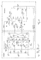
- Fig. 4 shows schematically the circuit diagram of a first embodiment of a balanced push-pull amplifier according to the invention.
- the two signal paths are symmetrically constructed and each contain a preamplifier block N1B and N2B and a power amplifier M1 and M2, respectively.
- the power amplifiers M1, M2 are each connected to one floating power supply V1, V2 connected, with the load circuits via a load RL, which is between the bases of the two power amplifiers M1, M2 is connected, are crossed over.
- the two bases of the power amplifier At the same time set the connection points or terminals RL1, RL2 for the externally connected load RL and form the signal output.
- the power supply of the preamplifier blocks N1B, N2B contains at least two series-connected voltage sources V3, V4, their connection point to ground GND is.
- the resulting supply voltages + Ub and -Ub feed the supply terminals of the preamplifier blocks, which in the embodiment of FIG. 4 each from an input side amplifier N1, N2 with high open-loop gain consist.
- the positive pole of the output stage of the amplifiers N1, N2 is positive Supply voltage + Ub or with another positive and also supplied ground-based voltage source.
- the negative pole of the output stage of the Amplifier N1, N2 is connected via a potential difference generator 4, 5 with the associated Load connection RL1, RL2 connected. About this potential difference generator 4, 5 flows an impressed current.
- the amplifier N1, N2 Due to the high idling gain in conjunction with a high-impedance non-inverting and high-impedance inverting input, with negligible offset voltage and negligible offset current and with a low-impedance output, the amplifier N1, N2 have a behavior like a more or less ideal op amp.
- the first power amplifier M1 is of a floating first Voltage source V1 and the second power amplifier M2 is a floating second voltage source V2 fed.
- the first power amplifier M1 is over its first supply terminal with a pole of the first voltage source V1 and over its second supply terminal, which also serves as a power amplifier output, with the first output RL1 and the load RL with the other pole of the first Voltage source V1 connected.
- the second power amplifier M2 is over its first Supply terminal with a pole of the second voltage source V2 and via its second supply terminal, which also serves as a power amplifier output, with the second output RL2 and via the load RL to the other pole of the second Voltage source V2 connected,
- the required operating point-determining control voltage is in the associated Potential difference generators 4, 5 by one of a quiescent current setting Ix determined with an adjustable current source I1 predetermined current, over the Potential difference generator 4, 5 generates the desired potential offset.
- the with the negative supply connection -Ub connected quiescent current setting device Ix contains an adjustable current source I1, whose current by means of the two with the Output terminals RL1, RL2 connected resistors R2, R3 in half on the two Potential difference generator 4, 5 is divided, so that the operating point setting for the two power amplifiers M1, M2 takes place symmetrically.
- this adjustment process can be done in different ways, For example, purely manually as in the embodiment of Fig. 4 via an adjustable Current source I1, an adjustable voltage source Vbias (see Fig. 8) or via a Potentiometer that controls the current source I1. It is also useful temperature-sensitive control, which has a temperature sensor that determines the temperature detected at least one power component, the adjustable current or Voltage source I1 or Vbias influenced so that the quiescent current of Power components of the power amplifier M1, M2 remains constant or one having predetermined temperature profile.
- the two amplifiers N1 and N2 have one inverting and one non-inverting one Input and correspond due to their high idle gain each one Operational amplifier.
- the load connection RL1 or RL2 which by a Feedback network is regulated to the ground potential GND.
- the Feedback network is through the series-connected resistors R6 and R7 or R8 and R9 formed between the load terminal RL1 and ground GND and the Load connection RL2 and ground GND are.
- the common connection point of the Resistors R6, R7 and R8, R9 is connected to the inverting input of the amplifier N1 or N2 connected.
- the non-inverting input of the first amplifier N1 is with the positive signal input + in and the non-inverting input of the second Amplifier N2 is connected to the negative signal input -in the push-pull amplifier connected.
- R6, R7 and R8, R9 is the output of the amplifier N1 or N2 regulated so that via the potential difference generator 4, 5 and the voltage divider R6, R7 and R8, R9 the potential at the non-inverting Input of the amplifier N1 or N2 identical to the potential at the positive or negative Signal input + in or -in is.
- This regulation over the feedback network is regardless of the size of the quiescent current setting for the power components of Power amplifier M1, M2, which is predetermined by the adjustable current source I1.
- the resulting level offset at the potential difference generator 4 and 5 is determined by the Amplifier N1 or N2 regulated.
- the resistors R10 and R11 from the positive and negative signal input to ground GND have no meaning for the feedback. They are only for determination the GND potential for the respective noninverting inputs of N1 and N2 and the line adaptation, since the signal inputs to the noninverting Inputs of amplifiers N1 and N2 are usually high impedance. Later will be one Embodiment shown in which the signal inputs to the inverting inputs the amplifiers N1 and N2 are connected. By the to these inputs connected feedback network, these inputs are then essential low impedance, so that a line adjustment may be omitted if necessary.
- the upper amplifier half essentially of the modules N1B and M1 consisting amplifies the one half-wave of the balanced input signal and the lower amplifier half, consisting of the modules N2B and M2, amplifies the another half wave.
- the power amplifiers M1, M2 can be practically implemented in a variety of ways: as individual power devices such as e.g. Power MOSFETs, IGBTs or bipolar Power transistors, but also advantageous combinations of the same or various amplifier components with or without local negative feedback.
- individual power devices such as e.g. Power MOSFETs, IGBTs or bipolar Power transistors, but also advantageous combinations of the same or various amplifier components with or without local negative feedback.
- the output stage of the preamplifier blocks N1B and N2B exemplified as triode Xtr1 or Xtr2 executed.
- the preamplifier blocks N1B and N2B each consist of the combination of a input side amplifier N1, N2 with high open-loop gain and one to the Amplifier N1, N2 connected tube Xtr1, Xtr2, whose control grid with the associated amplifier output is connected.
- the anode of the tube Xtr1, Xtr2 is with the positive supply voltage + Ub or with another positive and also mass-related voltage source connected.
- the cathode of the tube Xtr1, Xtr2 is over a potential difference generator 4, 5, which in the simplest case a resistor R4, R5 contains and over which an impressed current flows, with the associated load connection RL1, RL2 connected.
- tubes Xtr1, Xtr2 shown as triodes in the embodiment of FIG Of course, tetrodes, pentodes, hexodes and heptodes with the state of Technology corresponding wiring of the additional grid can be used.
- Fig. 5 As power amplifier M1, M2, two n-channel MOSFETs are shown in Fig. 5, whose respective gate electrode to the cathode of the preceding tube Xtr1, Xtr2 connected.
- the respective source electrode is connected to the associated load connection RL1, RL2 and the respective drain electrode with the positive potential of floating voltage source V1, V2 connected.
- the operating point-determining gate-source control voltage is in the associated potential difference generators 4, 5 by one of a quiescent current setting device Ix with an adjustable current source I1 predetermined current determined by the resistors R4, R5 the desired Potential offset generated.
- the one connected to the negative supply terminal -Ub Quiescent current adjuster Ix contains an adjustable current source I1 whose current by means of the two resistors connected to the output terminals RL1, RL2 R2, R3 is split in half on the two resistors R4, R5, so that the Operating point setting for the two MOSFETs M1, M2 takes place symmetrically.
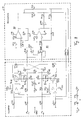
- Fig. 5 is schematically such a control arrangement as "Biasregelung" B1, which complements the push-pull amplifier of Fig. 4. Same thing Circuit and functional units in all figures of the drawing with the same Reference signs are provided, unnecessary repetitive descriptions of functions.
- the circuit block B1 contains two control circuits B2, B3 whose inputs are connected to the Amplifier outputs RL1, RL2 and their outputs with the feedback networks the two preamplifier blocks N1B and N2B are coupled.
- the input of the first control circuit B2 is equal by two connected in series Resistors R16, R17 are formed, which are connected to the outputs RL1, RL2 and their common connection point avg via a resistor R15 on the inverting input of an operational amplifier U3 is connected.
- a DC voltage V5 is applied at the non-inverting input of U3, a DC voltage V5 is applied.
- the exit of the amplifier U3 is by means of a capacitor C2 to the non-inverting Entrance returned.
- the power supply of the amplifier U3 takes place expediently via the already existing supply potentials + Ub and -Ub or via another supply voltage.
- the input of the second control loop B3 is formed by a subtractor D1, whose Minuendeingang + with the load terminal RL2 and its Subtrahendeingang - is connected to the load terminal RL1.
- the output of the subtracter D1 determines the potential of the node is diff and is connected to the inverting resistor R14 Input of an amplifier U4 connected via a capacitor C1 with his Amplifier output is connected. This output is also via a series circuit from an inverter N4 and a resistor R12 to the circuit node bias 1 and connected via a resistor R13 to the other circuit node bias 2.
- At the non-inverting input of the amplifier U4 is the ground potential GND connected.
- control block bias control B1 The function of the control block bias control B1 according to the invention is to that by means of the first control loop B2, the mean value avg of the potentials at the Outputs RL1, RL2 detected and compared with a predetermined target voltage V5 becomes.
- About the integrator formed by the amplifier U3 is the deviation of Potential avg amplified from the setpoint V5.
- the two directly coupled rule interfaces bias 1 and bias 2 indicate that the Average of the potentials at the output terminals RL1, RL2 to the predetermined Setpoint V5 is adjusted. This will be the magnitude of the absolute potential of the outputs RL1, RL2 defined set.
- ⁇ 2 greater than or equal to 1s makes sense.
- the amplifiers N1 or N2 in the preamplifier blocks realized so that in Hibernation a significant, also driftbelasteter, potential difference between the noninverting and the inverting input of these amplifiers N1, N2 occurs, so can by means of a suitable design of the bias control this disturbing influence on the Working point stability can be minimized.
- the first stage of a tube amplifier could be realized as a cathode base stage.
- the grid corresponds to the non-inverting input of the amplifier N1 or N2 and the cathode corresponds to the inverting input of N1 or N2.
- the operating points of tubes are thermal and aging-related fluctuations subjected. This changes the temperature and the aging of the input tubes, essentially the voltage gain in the amplifiers N1 and N2 cause the current component I (R6) or I (R8), and thus after the first relationship the by I (R4) certain potential of the gate-source path of the power amplifier M1. Accordingly, the potential determined by the current I (R5) has a negative effect on the Gate-source path of the power amplifier M2 off. To this disturbing influence to exclude or at least minimize the target voltage V5 is not fixed set, but as in the embodiment of Fig.
- These Node voltage avgln is connected through a resistor R26 to the noninverting Input of the control amplifier U3 out, the unlike in Fig. 5 not with a Reference voltage V5 is fed, but its reference voltage at this Connection itself generated by a capacitor C3 is connected there.
- bias 1 and bias 2 is thus over the RC element R26 and C3 low-pass filtered and then serves as a target voltage on non-inverting input of the control amplifier U3.
- the corner frequency of the RC element R26, C3 is preferably at least one decade lower than the lowest to be transferred Payload frequency selected.
- this circuit variant shown in Fig. 6 is the fundamental or drift - related potential difference between the inputs of the Amplifier N1 or N2, on the negative feedback network part of the Output voltage is returned, and the output node RL1 or RL2 ideal to Zero regulated or at least so small that with it the error portion of the Closed-circuit current control has no influence.
- FIG. 7 an embodiment of the push-pull amplifier is shown, as Power amplifiers M1, M2 each have tubes Xtr3, Xtr4, which directly drive the load RL.
- the preamp blocks N1B, N2B contain, unlike the previous ones Embodiments of FIG. 5 and FIG. 6 no combination amplifier, but consist solely of the amplifiers N1, N2. These are so realized that they are in the Hibernate a negative DC output voltage from a few volts to a few tens Volts depending on the connected tubes Xtr3, Xtr4 have.
- the adjustable Current source I1 is connected to a positive potential + Ub, so that half their Current through the resistors R2, R3, the level shifters 4, 5 and the internal Output stage from N1, N2 to negative supply voltage -Ub flows.
- This Current flow causes the necessary negative ones at the resistors R4, R5 Grid bias for tubes Xtr3 and Xtr4. It will be back with only one Control value of the quiescent current of both tubes Xtr3, Xtr4 in the floating without fixed Ground reference powered amplifiers M1, M2 defined and synchronous as well set symmetrically.
- the load RL in a special case by means of a transformer to the with Tubular equipped power amplifier M1, M2 can be coupled with the the same structure as in Fig. 7, except that then instead of the direct load coupling a transformer in a known manner to the internal resistance of the tube output stage the low-impedance load stepped down.
- the transformer can save costs be executed as autotransformer, since by the inventive Closed-circuit current setting no DC bias occurs.
- the autotransformer is wound symmetrically, for example in a two-chamber design, so that the same winding resistances result for both winding halves. Due to the lack of DC biasing is also a realization as a toroidal transformer possible.
- the winding will be the same as an integer Split parts, which are then wrapped in pairs bifilar.
- Symmetry principle for example, by simply winding up the respective Windings, still allows a stable operation of the invention Push-pull amplifier, but does not fully exploit its possibilities.
- FIG. 8 Another embodiment of the push-pull amplifier according to the invention shows Fig. 8.
- This circuit is almost identical to the circuit of Fig. 6, except that the Control value for the quiescent current setting not as in Fig. 6 by the adjustable Current source I1, but by an adjustable voltage source Vbias, the Ultimately via the resistors R2, R3 but also generates a current that means these resistors R2, R3 is divided in half and the resistors R4, R5 the desired operating point determining potential offset for the respective gate-source path of the two n-channel MOSFETs in the power amplifier M1, M2 generated.
- the absolute value of the potentials at the load terminals RL1, RL2 defined and adjusted to an approximately equal value. Since the resistors R2 and R3 are equal to each other, are also the flows flowing through them I (R2) and I (R3) equal to each other. These currents flow almost completely across the resistors R4 or R5 and from the cathode to the anode of the triode Xtr1 and Xtr2 to the positive Operating voltage + Ub. Due to the resulting potential offset on the resistors R4 or R5 becomes a defined positive potential difference between the gate-source path the MOSFETs M1 and M2 generated and thus flows logically a defined Quiescent current through these output stage transistors.
- the adjustment process of the voltage source Vbias can again be done in a variety of ways, manually, temperature controlled or by means of an automatic quiescent current control circuit.
- a push-pull amplifier according to the invention can also be realized by the input side amplifiers N1, N2 in the Pre-amplifier blocks N1B, N2B each with their inverting amplifier input on the signal inputs -in and + are connected in the push-pull amplifier.
- the input side amplifiers N1, N2 in the Pre-amplifier blocks N1B, N2B each with their inverting amplifier input on the signal inputs -in and + are connected in the push-pull amplifier.
- in the Input range of the amplifiers N1, N2 are only minor Make circuit changes.
- the resistors R7 and R9 of Feedback networks are now not connected to the ground potential as For example, in the comparable Fig. 5, but to the negative or positive Signal input -in or + in the push-pull amplifier.
- the resistors R10 and R11 on The non-inverting inputs of the amplifiers N1 and N2 are connected to the from the Amplifier opposite ends connected to the ground potential GND. Furthermore, the recirculated lines of the rule interfaces bias 1 and 2 bias no longer as in Fig.5 fed back to the inverting input of the amplifier N1 or N2, but on their non-inverting inputs. The recirculated from the control circuits B2 and B3 Control currents generate the necessary via the resistors R10 and R11 Control voltages for the amplifiers N1, N2.
- FIG. 10 shows a further variant of the quiescent current setting.
- the basic circuit of this push-pull amplifier is roughly comparable to the Circuit of Fig. 5.
- the potential difference generator 4 and 5 contain in addition to the Resistors R4 and R5 are each an optoelectronic device OK1 or OK2 or are coupled with such devices. Via a common current source I1 controlled the light emission of each one LED element, the intensity of which Volume resistance of a photosensitive photo-transistor is dependent.
- This Photo transistor is parallel to the already known from Fig. 5 resistor R4 or R5, which is fed via the likewise known resistor R2 or R3, whose Base point but in contrast to Fig. 5 on the negative fixed potential -Ub.
- the potential difference generators 4 and 5 respectively Thus formed by an assembly, the resistors R4 and R5 each with a Optokopplerrank OK1 or OK2 combined.
- a synchronous setting of the Quiescent current of both branches of the floating voltage supplied power amplifier takes place by the application of both optocouplers with the same control or Control current.
- the current equality is in the embodiment of FIG. 10 thereby forced, that the current of the adjustable current source I1 from the negative Supply connection -Ub through both optocouplers OK1, OK2 until positive Supply connection + Ub is looped through.
- the exemplary embodiment according to FIG. 11 shows an advantageous arrangement of the push-pull amplifier according to the invention when basically only unbalanced input signals are to be processed instead of symmetrical input signals.
- the circuit according to FIG. 5 is suitable.
- the amplifier N1 at the non-inverting input and the amplifier N2 at the inverting input are driven.
- the non-inverting input of the amplifier N1 is connected to the signal input + in and via the resistor R10 to the ground potential GND.
- the inverting input of the amplifier N1 is located at the voltage tap of the voltage divider R6, R7, as in FIG.
Landscapes
- Engineering & Computer Science (AREA)
- Power Engineering (AREA)
- Physics & Mathematics (AREA)
- Nonlinear Science (AREA)
- Amplifiers (AREA)
Abstract
Description
Die bisherigen Entwicklungen konzentrierten sich auf die Optimierung von reinen Transistorverstärkern einerseits und reinen Röhrenverstärkern andererseits. Daneben sind auch vereinzelt Verstärker mit hybrider Bauelementebestückung bekannt, die getrennt nach Röhren- bzw. Transistorverwendung optimierte Vor- und Leistungsverstärker enthalten, die in der Regel kapazitiv miteinander gekoppelt sind.
Claims (10)
- Verstärker in symmetrischer Gegentaktausführung mit einer ersten und dazu gleichen zweiten Verstärkungseinrichtung, wobei die erste Verstärkungseinrichtung (N1B, M1) in einem ersten Signalpfad zwischen einem ersten Eingang (+in) und einem ersten Ausgang (RL1) und eine zweite Verstärkungseinrichtung (N2B, M2) in einem zweiten Signalpfad zwischen einem zweiten Eingang (-in) und einem zweiten Ausgang (RL2) angeschlossen sind, weiterhin sind ein zu verstärkendes Signal an den ersten und/oder zweiten Eingang (+in, -in) und eine extern anzuschließende Last (RL) an den ersten und zweiten Ausgang (RL1, RL2) anschließbar,dadurch gekennzeichnet, dassder erste Eingang (+in) ist mit dem Signaleingang eines von einer Spannungsversorgungseinrichtung (V3, V4) gespeisten ersten Vorverstärkerblocks (N1B) und dessen Ausgang mit dem Signaleingang eines ersten Endverstärkers (M1) gekoppelt, und der zweite Eingang (-in) ist mit dem Signaleingang eines von der Spannungsversorgungseinrichtung (V3, V4) gespeisten zweiten Vorverstärkerblocks (N2B) und dessen Ausgang mit dem Signaleingang eines zweiten Endverstärkers (M2) gekoppelt,der erste Endverstärker (M1) ist von einer schwimmenden ersten Spannungsquelle (V1) und der zweite Endverstärker (M2) von einer schwimmenden zweiten Spannungsquelle (V2) gespeist,der erste Endverstärker (M1) ist über seinen ersten Versorgungsanschluss mit einem Pol der ersten Spannungsquelle (V1) und über seinen zweiten Versorgungsanschluss, der auch als Endverstärkerausgang dient, mit dem ersten Ausgang (RL1) und über die Last (RL) mit dem anderen Pol der ersten Spannungsquelle (V1) verbunden, undder zweite Endverstärker (M2) ist über seinen ersten Versorgungsanschluss mit einem Pol der zweiten Spannungsquelle (V2) und über seinen zweiten Versorgungsanschluss, der auch als Endverstärkerausgang dient, mit dem zweiten Ausgang (RL2) und über die Last (RL) mit dem anderen Pol der zweiten Spannungsquelle (V2) verbunden,ein erster Potentialdifferenzerzeuger (4) zwischen dem Ausgang des ersten Vorverstärkerblocks (N1B) und dem ersten Ausgang (RL1) in Abhängigkeit von einer Ruhestromeinstelleinrichtung (Ix) eine erste Differenzspannung zwischen dem Ausgang des ersten Vorverstärkerblocks (N1B) und dem ersten Ausgang (RL1) erzeugt, die den Arbeitspunkt und den Ruhestrom des ersten Endverstärkers (M1) bestimmt undein zweiter Potentialdifferenzerzeuger (5) zwischen dem Ausgang des zweiten Vorverstärkerblocks (N2B) und dem zweiten Ausgang (RL2) in Abhängigkeit von der Ruhestromeinstelleinrichtung (Ix) eine zweite Differenzspannung zwischen dem Ausgang des zweiten Vorverstärkerblocks (N2B) und dem zweiten Ausgang (RL2) erzeugt, die den Arbeitspunkt und den Ruhestrom des zweiten Endverstärkers (M2) einstellt.
- Verstärker nach Anspruch 1, dadurch gekennzeichnet, dass der erste und zweite Vorverstärkerblock (N1B, N2B) Röhren und/oder Halbleiter enthält und die ausgangsseitige Spannungsanpassung an den ersten und zweiten Endverstärker (M1, M2) mittels des zugeordneten ersten und zweiten Potentialdifferenzerzeugers (4, 5) in Verbindung mit der Ruhestromeinstelleinrichtung (Ix) erfolgt.
- Verstärker nach Anspruch 2, dadurch gekennzeichnet, dass zusätzlich zu dem ersten und zweiten Verstärkerblock (N1B, N2B) eine Regeleinrichtung (B1) in Abhängigkeit von den Offsetspannungen an dem ersten und zweiten Ausgang (RL1, RL2) Korrektursignale (bias2, bias1) dem ersten und/oder zweiten Verstärkerblock (N1B, N2B) zuführt und damit Offsetspannungen an dem ersten und zweiten Ausgang (RL1, RL2) beseitigt oder zumindest verkleinert.
- Verstärker nach Anspruch 3, dadurch gekennzeichnet, dass die Regeleinrichtung (B1) eine erste Regeleinheit (B2) enthält, der als Istwert ein von den Gleichspannungsarbeitspunkten des ersten und zweiten Ausgangs (RL1, RL2) abhängiges Signal (avg) und als Sollwert ein vorgegebener Gleichspannungspegel (V5) zugeführt sind.
- Verstärker nach Anspruch 3 oder 4, dadurch gekennzeichnet, dass die Regeleinrichtung (B1) eine zweite Regeleinheit (B3) enthält, der als Istwert die Spannungsdifferenz (diff) zwischen dem ersten und zweiten Ausgang (RL1, RL2) zugeführt ist, wobei als Sollwert der Spannungsdifferenz-Nullwert dient.
- Verstärker nach Anspruch 5, dadurch gekennzeichnet, dass die Regeleinrichtung (B1) eine dritte Regeleinheit (B4) enthält, so dass der vorgegebene Gleichspannungspegel mittels einer Filtereinrichtung aus dem Potentialmittelwert des ersten und zweiten Eingangs (+in, -in) gebildet ist.
- Verstärker nach Anspruch 5, dadurch gekennzeichnet, dass der vorgegebene Gleichspannungspegel für die erste Regeleinheit (B2) mittels einer Filtereinrichtung (R26, C3) aus dem Potentialmittelwert (avgin) derjenigen Eingänge des ersten und zweiten Vorverstärkerblocks (N1B, N2B) gebildet ist, die jeweils über ein Gegenkopplungsnetzwerk mit dem ersten bzw. zweiten Ausgang (RL1, RL2) verbunden sind.
- Verstärker nach mindestens einem der Ansprüche 1 bis 7, dadurch gekennzeichnet, dass die Ruhestromeinstelleinrichtung (Ix) den Ruhestrom für den ersten und zweiten Endverstärker (M1, M2) mittels eines temperaturabhängigen Steuerwerts einstellt, wobei die Temperatur insbesondere im Bereich der Endverstärker bestimmt ist.
- Verstärker nach mindestens einem der Ansprüche 1 bis 7, dadurch gekennzeichnet, dass die Ruhestromeinstelleinrichtung (Ix) einen Regler enthält, der den Istwert des Ruhestroms mindestens eines Endverstärkers (M1, M2) misst und auf einen Sollwert nachregelt.
- Verstärker nach mindestens einem der Ansprüche 1 bis 8, dadurch gekennzeichnet, dass lokale Gegenkopplungen und/oder Kompensationsmaßnahmen in den beiden Signalpfaden der Verbesserung des linearen Übertragungsverhaltens dienen.
Applications Claiming Priority (2)
| Application Number | Priority Date | Filing Date | Title |
|---|---|---|---|
| DE10360347 | 2003-12-22 | ||
| DE10360347A DE10360347A1 (de) | 2003-12-22 | 2003-12-22 | Symmetrischer Gegentaktverstärker |
Publications (2)
| Publication Number | Publication Date |
|---|---|
| EP1548934A1 true EP1548934A1 (de) | 2005-06-29 |
| EP1548934B1 EP1548934B1 (de) | 2008-09-03 |
Family
ID=34530345
Family Applications (1)
| Application Number | Title | Priority Date | Filing Date |
|---|---|---|---|
| EP04030390A Expired - Lifetime EP1548934B1 (de) | 2003-12-22 | 2004-12-22 | Vollsymmetrischer Leistungsverstärker |
Country Status (3)
| Country | Link |
|---|---|
| EP (1) | EP1548934B1 (de) |
| AT (1) | ATE407478T1 (de) |
| DE (2) | DE10360347A1 (de) |
Families Citing this family (2)
| Publication number | Priority date | Publication date | Assignee | Title |
|---|---|---|---|---|
| DE102008025347B4 (de) * | 2007-12-22 | 2015-07-09 | Klaus Zametzky | Elektronischer Verstärker |
| US10320343B1 (en) | 2018-03-08 | 2019-06-11 | Real Analog, Llc | Amplifier output stage using toroidal transformer |
Citations (5)
| Publication number | Priority date | Publication date | Assignee | Title |
|---|---|---|---|---|
| US4229706A (en) * | 1979-01-05 | 1980-10-21 | Bongiorno James W | Audio amplifier |
| FR2547470A1 (fr) * | 1983-06-08 | 1984-12-14 | Scherer Rene | Regulateur de courant de polarisation pour amplificateurs a symetrie complementaire et etages de sortie utilisant ce regulateur |
| US4531100A (en) * | 1981-11-10 | 1985-07-23 | Adkin Francis W | Amplifier suitable for low supply voltage operation |
| WO2000011779A1 (en) * | 1998-08-19 | 2000-03-02 | Ryszard Parosa | Circuit for precise sensing and regulation of quiescent dc current in transistor power amplifiers |
| US6242977B1 (en) * | 1999-05-26 | 2001-06-05 | Atma-Sphere Music Systems, Inc. | Amplifier and preamplifier circuit |
Family Cites Families (2)
| Publication number | Priority date | Publication date | Assignee | Title |
|---|---|---|---|---|
| US4719431A (en) * | 1986-04-21 | 1988-01-12 | Karsten Ralph R | Audio power amplifier |
| GB2305039B (en) * | 1994-07-13 | 1998-12-30 | Bhc Consulting Pty Ltd | An improvement to amplifiers |
-
2003
- 2003-12-22 DE DE10360347A patent/DE10360347A1/de not_active Withdrawn
-
2004
- 2004-12-22 EP EP04030390A patent/EP1548934B1/de not_active Expired - Lifetime
- 2004-12-22 AT AT04030390T patent/ATE407478T1/de active
- 2004-12-22 DE DE502004007977T patent/DE502004007977D1/de not_active Expired - Lifetime
Patent Citations (5)
| Publication number | Priority date | Publication date | Assignee | Title |
|---|---|---|---|---|
| US4229706A (en) * | 1979-01-05 | 1980-10-21 | Bongiorno James W | Audio amplifier |
| US4531100A (en) * | 1981-11-10 | 1985-07-23 | Adkin Francis W | Amplifier suitable for low supply voltage operation |
| FR2547470A1 (fr) * | 1983-06-08 | 1984-12-14 | Scherer Rene | Regulateur de courant de polarisation pour amplificateurs a symetrie complementaire et etages de sortie utilisant ce regulateur |
| WO2000011779A1 (en) * | 1998-08-19 | 2000-03-02 | Ryszard Parosa | Circuit for precise sensing and regulation of quiescent dc current in transistor power amplifiers |
| US6242977B1 (en) * | 1999-05-26 | 2001-06-05 | Atma-Sphere Music Systems, Inc. | Amplifier and preamplifier circuit |
Also Published As
| Publication number | Publication date |
|---|---|
| DE10360347A1 (de) | 2005-07-21 |
| DE502004007977D1 (de) | 2008-10-16 |
| ATE407478T1 (de) | 2008-09-15 |
| EP1548934B1 (de) | 2008-09-03 |
Similar Documents
| Publication | Publication Date | Title |
|---|---|---|
| DE69207612T2 (de) | Frequenzkompensierter Mehrstufenverstärker mit verschachtelter kapazitiver Neutralisierung und innerer Mehrweg-Vorwärtssteuerung | |
| DE112012000470B4 (de) | Vorrichtung und Verfahren zur Miller-Kompensation bei mehrstufigen Verstärkern | |
| EP0579686A1 (de) | Wandlerschaltung. | |
| DE69023061T2 (de) | Pufferverstärker mit niedrigem Ausgangswiderstand. | |
| DE112017001304T5 (de) | Aktive Linearisierung für Breitbandverstärker | |
| DE3043952A1 (de) | Gegentakt-ab-verstaerker | |
| DE3011933C2 (de) | Leistungsverstärker | |
| DE102013109957B4 (de) | Schaltung zum Verhindern von lastinduzierter Nichtlinearität in Operationsverstärkern | |
| DE102014003232B4 (de) | Hocheffiziente ultra-lineare A-Klasse-Ausgangsstufe | |
| DE3011835A1 (de) | Leistungsverstaerker | |
| DE4122057A1 (de) | Rueckkopplungssteuerung zur verringerung der durch eine differenzverstaerkerstufe hervorgerufenen signalverzerrung | |
| DE10351593B4 (de) | Integrierte Vorverstärkerschaltung für die Erfassung eines Signalstroms von einer Photodiode | |
| DE10128570B4 (de) | Verbesserte Anstiegsgeschwindigkeit in Verstärkerschaltungen | |
| DE102005054216A1 (de) | Ausgangsstufe, Verstärkerregelschleife und Verwendung der Ausgangsstufe | |
| EP1548934B1 (de) | Vollsymmetrischer Leistungsverstärker | |
| EP3631978A1 (de) | Transimpedanzverstärker-schaltung | |
| JP3081210B2 (ja) | 線形利得増幅回路 | |
| DE19962811B4 (de) | Gegentaktverstärkerschaltung | |
| DE102008025347B4 (de) | Elektronischer Verstärker | |
| DE102011054423A1 (de) | Akustische pseudo-triodencharakteristik-verstärkungsvorrichtung und akustische pseudo-triodencharakteristik-push-pull-verstärkungsvorrichtung | |
| US7961049B2 (en) | Amplifier with compensated gate bias | |
| DE3007715A1 (de) | Verstaerkerschaltung mit durch eine steuerspannung steuerbarer gesamtverstaerkung | |
| EP1101279A1 (de) | Verstärkerausgangsstufe | |
| DE3305482A1 (de) | Durch vormagnetisierungsstrom kompensierter verstaerker | |
| EP0632580A2 (de) | Verstärkerausgangsstufe |
Legal Events
| Date | Code | Title | Description |
|---|---|---|---|
| PUAI | Public reference made under article 153(3) epc to a published international application that has entered the european phase |
Free format text: ORIGINAL CODE: 0009012 |
|
| AK | Designated contracting states |
Kind code of ref document: A1 Designated state(s): AT BE BG CH CY CZ DE DK EE ES FI FR GB GR HU IE IS IT LI LT LU MC NL PL PT RO SE SI SK TR |
|
| AX | Request for extension of the european patent |
Extension state: AL BA HR LV MK YU |
|
| 17P | Request for examination filed |
Effective date: 20051223 |
|
| AKX | Designation fees paid |
Designated state(s): AT BE BG CH CY CZ DE DK EE ES FI FR GB GR HU IE IS IT LI LT LU MC NL PL PT RO SE SI SK TR |
|
| 17Q | First examination report despatched |
Effective date: 20061211 |
|
| GRAP | Despatch of communication of intention to grant a patent |
Free format text: ORIGINAL CODE: EPIDOSNIGR1 |
|
| GRAS | Grant fee paid |
Free format text: ORIGINAL CODE: EPIDOSNIGR3 |
|
| GRAA | (expected) grant |
Free format text: ORIGINAL CODE: 0009210 |
|
| AK | Designated contracting states |
Kind code of ref document: B1 Designated state(s): AT BE BG CH CY CZ DE DK EE ES FI FR GB GR HU IE IS IT LI LT LU MC NL PL PT RO SE SI SK TR |
|
| REG | Reference to a national code |
Ref country code: GB Ref legal event code: FG4D Free format text: NOT ENGLISH |
|
| REG | Reference to a national code |
Ref country code: CH Ref legal event code: EP |
|
| REG | Reference to a national code |
Ref country code: IE Ref legal event code: FG4D Free format text: LANGUAGE OF EP DOCUMENT: GERMAN |
|
| REF | Corresponds to: |
Ref document number: 502004007977 Country of ref document: DE Date of ref document: 20081016 Kind code of ref document: P |
|
| PG25 | Lapsed in a contracting state [announced via postgrant information from national office to epo] |
Ref country code: LT Free format text: LAPSE BECAUSE OF FAILURE TO SUBMIT A TRANSLATION OF THE DESCRIPTION OR TO PAY THE FEE WITHIN THE PRESCRIBED TIME-LIMIT Effective date: 20080903 Ref country code: NL Free format text: LAPSE BECAUSE OF FAILURE TO SUBMIT A TRANSLATION OF THE DESCRIPTION OR TO PAY THE FEE WITHIN THE PRESCRIBED TIME-LIMIT Effective date: 20080903 Ref country code: ES Free format text: LAPSE BECAUSE OF FAILURE TO SUBMIT A TRANSLATION OF THE DESCRIPTION OR TO PAY THE FEE WITHIN THE PRESCRIBED TIME-LIMIT Effective date: 20081214 |
|
| PG25 | Lapsed in a contracting state [announced via postgrant information from national office to epo] |
Ref country code: FI Free format text: LAPSE BECAUSE OF FAILURE TO SUBMIT A TRANSLATION OF THE DESCRIPTION OR TO PAY THE FEE WITHIN THE PRESCRIBED TIME-LIMIT Effective date: 20080903 Ref country code: SI Free format text: LAPSE BECAUSE OF FAILURE TO SUBMIT A TRANSLATION OF THE DESCRIPTION OR TO PAY THE FEE WITHIN THE PRESCRIBED TIME-LIMIT Effective date: 20080903 |
|
| NLV1 | Nl: lapsed or annulled due to failure to fulfill the requirements of art. 29p and 29m of the patents act | ||
| REG | Reference to a national code |
Ref country code: IE Ref legal event code: FD4D |
|
| PG25 | Lapsed in a contracting state [announced via postgrant information from national office to epo] |
Ref country code: BG Free format text: LAPSE BECAUSE OF FAILURE TO SUBMIT A TRANSLATION OF THE DESCRIPTION OR TO PAY THE FEE WITHIN THE PRESCRIBED TIME-LIMIT Effective date: 20081203 Ref country code: IE Free format text: LAPSE BECAUSE OF FAILURE TO SUBMIT A TRANSLATION OF THE DESCRIPTION OR TO PAY THE FEE WITHIN THE PRESCRIBED TIME-LIMIT Effective date: 20080903 |
|
| PG25 | Lapsed in a contracting state [announced via postgrant information from national office to epo] |
Ref country code: RO Free format text: LAPSE BECAUSE OF FAILURE TO SUBMIT A TRANSLATION OF THE DESCRIPTION OR TO PAY THE FEE WITHIN THE PRESCRIBED TIME-LIMIT Effective date: 20080903 Ref country code: SK Free format text: LAPSE BECAUSE OF FAILURE TO SUBMIT A TRANSLATION OF THE DESCRIPTION OR TO PAY THE FEE WITHIN THE PRESCRIBED TIME-LIMIT Effective date: 20080903 Ref country code: CZ Free format text: LAPSE BECAUSE OF FAILURE TO SUBMIT A TRANSLATION OF THE DESCRIPTION OR TO PAY THE FEE WITHIN THE PRESCRIBED TIME-LIMIT Effective date: 20080903 Ref country code: IS Free format text: LAPSE BECAUSE OF FAILURE TO SUBMIT A TRANSLATION OF THE DESCRIPTION OR TO PAY THE FEE WITHIN THE PRESCRIBED TIME-LIMIT Effective date: 20090103 Ref country code: PT Free format text: LAPSE BECAUSE OF FAILURE TO SUBMIT A TRANSLATION OF THE DESCRIPTION OR TO PAY THE FEE WITHIN THE PRESCRIBED TIME-LIMIT Effective date: 20090203 |
|
| BERE | Be: lapsed |
Owner name: BLOHBAUM, FRANK Effective date: 20081231 |
|
| PLBE | No opposition filed within time limit |
Free format text: ORIGINAL CODE: 0009261 |
|
| STAA | Information on the status of an ep patent application or granted ep patent |
Free format text: STATUS: NO OPPOSITION FILED WITHIN TIME LIMIT |
|
| PG25 | Lapsed in a contracting state [announced via postgrant information from national office to epo] |
Ref country code: MC Free format text: LAPSE BECAUSE OF NON-PAYMENT OF DUE FEES Effective date: 20081231 Ref country code: EE Free format text: LAPSE BECAUSE OF FAILURE TO SUBMIT A TRANSLATION OF THE DESCRIPTION OR TO PAY THE FEE WITHIN THE PRESCRIBED TIME-LIMIT Effective date: 20080903 Ref country code: DK Free format text: LAPSE BECAUSE OF FAILURE TO SUBMIT A TRANSLATION OF THE DESCRIPTION OR TO PAY THE FEE WITHIN THE PRESCRIBED TIME-LIMIT Effective date: 20080903 |
|
| 26N | No opposition filed |
Effective date: 20090604 |
|
| PG25 | Lapsed in a contracting state [announced via postgrant information from national office to epo] |
Ref country code: IT Free format text: LAPSE BECAUSE OF FAILURE TO SUBMIT A TRANSLATION OF THE DESCRIPTION OR TO PAY THE FEE WITHIN THE PRESCRIBED TIME-LIMIT Effective date: 20080903 |
|
| PG25 | Lapsed in a contracting state [announced via postgrant information from national office to epo] |
Ref country code: BE Free format text: LAPSE BECAUSE OF NON-PAYMENT OF DUE FEES Effective date: 20081231 |
|
| PG25 | Lapsed in a contracting state [announced via postgrant information from national office to epo] |
Ref country code: SE Free format text: LAPSE BECAUSE OF FAILURE TO SUBMIT A TRANSLATION OF THE DESCRIPTION OR TO PAY THE FEE WITHIN THE PRESCRIBED TIME-LIMIT Effective date: 20081203 |
|
| PGFP | Annual fee paid to national office [announced via postgrant information from national office to epo] |
Ref country code: FR Payment date: 20100107 Year of fee payment: 6 |
|
| PG25 | Lapsed in a contracting state [announced via postgrant information from national office to epo] |
Ref country code: PL Free format text: LAPSE BECAUSE OF FAILURE TO SUBMIT A TRANSLATION OF THE DESCRIPTION OR TO PAY THE FEE WITHIN THE PRESCRIBED TIME-LIMIT Effective date: 20080903 |
|
| PG25 | Lapsed in a contracting state [announced via postgrant information from national office to epo] |
Ref country code: LU Free format text: LAPSE BECAUSE OF NON-PAYMENT OF DUE FEES Effective date: 20081222 Ref country code: HU Free format text: LAPSE BECAUSE OF FAILURE TO SUBMIT A TRANSLATION OF THE DESCRIPTION OR TO PAY THE FEE WITHIN THE PRESCRIBED TIME-LIMIT Effective date: 20090304 Ref country code: CY Free format text: LAPSE BECAUSE OF FAILURE TO SUBMIT A TRANSLATION OF THE DESCRIPTION OR TO PAY THE FEE WITHIN THE PRESCRIBED TIME-LIMIT Effective date: 20080903 |
|
| PG25 | Lapsed in a contracting state [announced via postgrant information from national office to epo] |
Ref country code: TR Free format text: LAPSE BECAUSE OF FAILURE TO SUBMIT A TRANSLATION OF THE DESCRIPTION OR TO PAY THE FEE WITHIN THE PRESCRIBED TIME-LIMIT Effective date: 20080903 |
|
| PG25 | Lapsed in a contracting state [announced via postgrant information from national office to epo] |
Ref country code: GR Free format text: LAPSE BECAUSE OF FAILURE TO SUBMIT A TRANSLATION OF THE DESCRIPTION OR TO PAY THE FEE WITHIN THE PRESCRIBED TIME-LIMIT Effective date: 20081204 |
|
| PGFP | Annual fee paid to national office [announced via postgrant information from national office to epo] |
Ref country code: CH Payment date: 20110315 Year of fee payment: 7 |
|
| PGFP | Annual fee paid to national office [announced via postgrant information from national office to epo] |
Ref country code: GB Payment date: 20110114 Year of fee payment: 7 |
|
| REG | Reference to a national code |
Ref country code: FR Ref legal event code: ST Effective date: 20110831 |
|
| PG25 | Lapsed in a contracting state [announced via postgrant information from national office to epo] |
Ref country code: FR Free format text: LAPSE BECAUSE OF NON-PAYMENT OF DUE FEES Effective date: 20110103 |
|
| REG | Reference to a national code |
Ref country code: CH Ref legal event code: PL |
|
| GBPC | Gb: european patent ceased through non-payment of renewal fee |
Effective date: 20111222 |
|
| PG25 | Lapsed in a contracting state [announced via postgrant information from national office to epo] |
Ref country code: GB Free format text: LAPSE BECAUSE OF NON-PAYMENT OF DUE FEES Effective date: 20111222 Ref country code: CH Free format text: LAPSE BECAUSE OF NON-PAYMENT OF DUE FEES Effective date: 20111231 Ref country code: LI Free format text: LAPSE BECAUSE OF NON-PAYMENT OF DUE FEES Effective date: 20111231 |
|
| PGFP | Annual fee paid to national office [announced via postgrant information from national office to epo] |
Ref country code: AT Payment date: 20121228 Year of fee payment: 9 |
|
| PGFP | Annual fee paid to national office [announced via postgrant information from national office to epo] |
Ref country code: DE Payment date: 20131230 Year of fee payment: 10 |
|
| REG | Reference to a national code |
Ref country code: AT Ref legal event code: MM01 Ref document number: 407478 Country of ref document: AT Kind code of ref document: T Effective date: 20131222 |
|
| PG25 | Lapsed in a contracting state [announced via postgrant information from national office to epo] |
Ref country code: AT Free format text: LAPSE BECAUSE OF NON-PAYMENT OF DUE FEES Effective date: 20131222 |
|
| REG | Reference to a national code |
Ref country code: DE Ref legal event code: R119 Ref document number: 502004007977 Country of ref document: DE |
|
| PG25 | Lapsed in a contracting state [announced via postgrant information from national office to epo] |
Ref country code: DE Free format text: LAPSE BECAUSE OF NON-PAYMENT OF DUE FEES Effective date: 20150701 |