EP1548877B1 - Multibandantenne mit planaren Strahlerflächen und tragbares Telefon mit einer derartigen Antenne - Google Patents
Multibandantenne mit planaren Strahlerflächen und tragbares Telefon mit einer derartigen Antenne Download PDFInfo
- Publication number
- EP1548877B1 EP1548877B1 EP04293084.2A EP04293084A EP1548877B1 EP 1548877 B1 EP1548877 B1 EP 1548877B1 EP 04293084 A EP04293084 A EP 04293084A EP 1548877 B1 EP1548877 B1 EP 1548877B1
- Authority
- EP
- European Patent Office
- Prior art keywords
- radiation
- antenna according
- switches
- antenna
- mhz
- Prior art date
- Legal status (The legal status is an assumption and is not a legal conclusion. Google has not performed a legal analysis and makes no representation as to the accuracy of the status listed.)
- Ceased
Links
- 230000005855 radiation Effects 0.000 claims description 57
- 238000004891 communication Methods 0.000 claims description 6
- 238000010295 mobile communication Methods 0.000 claims description 6
- 230000005540 biological transmission Effects 0.000 claims description 4
- 230000005669 field effect Effects 0.000 claims description 4
- 238000000034 method Methods 0.000 description 5
- 239000003795 chemical substances by application Substances 0.000 description 4
- 230000006978 adaptation Effects 0.000 description 3
- 230000015572 biosynthetic process Effects 0.000 description 3
- 238000011161 development Methods 0.000 description 3
- 230000018109 developmental process Effects 0.000 description 3
- 239000003990 capacitor Substances 0.000 description 2
- 230000001939 inductive effect Effects 0.000 description 2
- 238000002955 isolation Methods 0.000 description 2
- 239000004065 semiconductor Substances 0.000 description 2
- 230000035939 shock Effects 0.000 description 2
- 229920002472 Starch Polymers 0.000 description 1
- 230000003044 adaptive effect Effects 0.000 description 1
- 230000000903 blocking effect Effects 0.000 description 1
- 230000009977 dual effect Effects 0.000 description 1
- 238000005516 engineering process Methods 0.000 description 1
- 230000010354 integration Effects 0.000 description 1
- 238000005259 measurement Methods 0.000 description 1
- 238000004377 microelectronic Methods 0.000 description 1
- 230000002093 peripheral effect Effects 0.000 description 1
- 238000000926 separation method Methods 0.000 description 1
- 235000019698 starch Nutrition 0.000 description 1
- 239000008107 starch Substances 0.000 description 1
Images


Classifications
-
- H—ELECTRICITY
- H01—ELECTRIC ELEMENTS
- H01Q—ANTENNAS, i.e. RADIO AERIALS
- H01Q9/00—Electrically-short antennas having dimensions not more than twice the operating wavelength and consisting of conductive active radiating elements
- H01Q9/04—Resonant antennas
- H01Q9/0407—Substantially flat resonant element parallel to ground plane, e.g. patch antenna
- H01Q9/0421—Substantially flat resonant element parallel to ground plane, e.g. patch antenna with a shorting wall or a shorting pin at one end of the element
-
- H—ELECTRICITY
- H01—ELECTRIC ELEMENTS
- H01Q—ANTENNAS, i.e. RADIO AERIALS
- H01Q1/00—Details of, or arrangements associated with, antennas
- H01Q1/12—Supports; Mounting means
- H01Q1/22—Supports; Mounting means by structural association with other equipment or articles
- H01Q1/24—Supports; Mounting means by structural association with other equipment or articles with receiving set
- H01Q1/241—Supports; Mounting means by structural association with other equipment or articles with receiving set used in mobile communications, e.g. GSM
- H01Q1/242—Supports; Mounting means by structural association with other equipment or articles with receiving set used in mobile communications, e.g. GSM specially adapted for hand-held use
-
- H—ELECTRICITY
- H01—ELECTRIC ELEMENTS
- H01Q—ANTENNAS, i.e. RADIO AERIALS
- H01Q23/00—Antennas with active circuits or circuit elements integrated within them or attached to them
-
- H—ELECTRICITY
- H01—ELECTRIC ELEMENTS
- H01Q—ANTENNAS, i.e. RADIO AERIALS
- H01Q9/00—Electrically-short antennas having dimensions not more than twice the operating wavelength and consisting of conductive active radiating elements
- H01Q9/04—Resonant antennas
- H01Q9/0407—Substantially flat resonant element parallel to ground plane, e.g. patch antenna
- H01Q9/0442—Substantially flat resonant element parallel to ground plane, e.g. patch antenna with particular tuning means
-
- H—ELECTRICITY
- H01—ELECTRIC ELEMENTS
- H01Q—ANTENNAS, i.e. RADIO AERIALS
- H01Q9/00—Electrically-short antennas having dimensions not more than twice the operating wavelength and consisting of conductive active radiating elements
- H01Q9/04—Resonant antennas
- H01Q9/06—Details
- H01Q9/14—Length of element or elements adjustable
- H01Q9/145—Length of element or elements adjustable by varying the electrical length
Definitions
- the present invention relates to an antenna of the type with radiating surface (s) plane (s).
- the invention proposes in particular an antenna of this type capable of being used in transmission / reception over at least two frequency bands, and having improved performances compared to antennas of the state of the art.
- planar antennas called PIFA ("Planar Inverted-F Antenna” or flat antenna type F inverted) which comprise, as illustrated by the figure 1 , a ground plane 1 and a flat conductive surface 2 which is superimposed on this ground plane 1, and extends to the right and parallel thereto.
- PIFA Planar Inverted-F Antenna
- Such an arrangement has a resonance wavelength which is a function of the dimensions of the plane conductive surface 2 and the height which separates it from its ground plane 1.
- the planar conductive surface 2 comprises a current driving point A and a grounding plane G.
- the resonance frequency is notably related to the greatest peripheral length L AG between the point A and the point G, the length L AG being referenced by 3 on the figure 1 .
- the length h is also added to L AG twice to obtain a length making it possible to find the resonant frequency of the antenna.
- These antennas have a particular advantage in terms of congestion and integration ability in mobile phones.
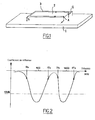
- FIGS. 3A to 3C show that we know antennas for radiating on several frequencies.
- the low resonant frequency is defined by the length denoted by L B and the high resonance frequency by the length denoted L H.
- L B we define L B by the longest path on surface 2 to go from A to G, to which the distance h is added twice.
- L H by an equivalent dimension of the slot to which we add twice the distance h.
- the calculation of L H is known to those skilled in the art.
- the figure 4 shows that we also know transmitting / receiving multiband antennas having at least one plane 2 radiation surface having two slots 30 separating radiation sections 21, 22 and 23.
- the radiation sections 21, 22 and 23 are connected by means Z 1 and Z 2 defining adaptive passive circuits known to those skilled in the art which, on transmission as on reception, are resonant on simultaneously at least two frequency bands.
- the means Z 1 and Z 2 define passive matching circuits and are generally connected in parallel with capacitive or inductive means themselves connected in series with means able to be switched selectively between a passing state and a starch. blocked.
- the capacitive or inductive means offset the resonance bands of the antenna, depending on whether the means capable of being switched are in the on state or in the off state.
- the means Z 1 and Z 2 comprise a plug circuit known to those skilled in the art which will be equivalent to an inductor for the low frequencies and a capacity for the high frequencies.
- the antennas Figures 3A to 4 provide acceptable radiation performance, especially in far-field measurement, while locally producing a lower near field than whip antennas or helical antennas otherwise known.
- the antennas of the state of the art of Figures 3A to 4 are designed in such a way that multiband performance is average in the different bands.
- US Patent 4780724 discloses a switch control technique, however the switches are connected to the ground plane.
- the invention proposes to overcome these disadvantages.
- An object of the invention is to overcome at least one of the disadvantages of antennas of the prior art.
- one of the aims of the invention is to propose an antenna for which multiband performance is very close to several single-band antennas.
- Another object of the invention is to provide an antenna having a plurality of resonance bands and having a very large bandwidth with respect to the multiband antennas of the state of the art.
- Another object of the invention is to provide an antenna having a plurality of resonance bands and having a very high yield compared to the multiband antennas of the state of the art.
- One of the other aims of the invention is to propose an antenna comprising several resonance bands, at least one of which is in the GSM domain and at least one in the DCS 1800 domain, the antenna compensating for at least one of the disadvantages of the antennas. the prior art.
- the invention provides an antenna according to claim 1.
- control current of the switches arrives at the antenna by the point of attack.
- the invention also relates to a telephone comprising an antenna according to the invention.
- the transmitting / receiving antenna shown on the figure 5 comprises a ground plane 1 and a plane radiating surface 2 which extends superimposed on said ground plane 1, being parallel thereto.
- An antenna according to the invention may also comprise more than one plane radiating surface.
- the radiating surface 2 is connected on one side to the ground plane 1 (connection point G) and on the other side to an RF signal supply / reception electronics (connection point A).
- the radiation surface 2 is divided into at least two radiation zones 51 and 52 separated by a junction 4 formed over most of its length with a slot.
- the radiation surface 2 may of course have more than two radiation zones 51 and 52 and more than one junction 4.
- the ends of the junction 4 located on the periphery 7 of the radiation surface 2 comprise means 60 forming mechanical links and forming electrical switches between the radiation zones 51 and 52.
- the electrical switches 60 are able to resonate all or part of the radiation surface 2 by electrically connecting all or part of the radiation zones.
- the figure 5 shows that at least the radiation zone 51 comprises at least one radiation slot 5.
- the opening 6 of the slot 5 is located at the periphery 7 of the radiation surface 2.
- the figure 5 thus shows that the opening 6 of the slot 5 comprises means 61 able to form a mechanical connection between the two sides of the slot 5 at the periphery 7 of the radiation surface 2.
- the means 61 also form electrical switches between these two sides.
- the means 61 are able to allow the flow of current on the periphery 7 of the radiation surface 2 in a closed electrical state, or to allow the flow of current on the inner periphery 8 of the slot 5 in an open electrical state.
- the surface of the figure 5 is equivalent to a radiating surface 2 as represented on the Figure 6A . All radiation zones are electrically connected to each other.
- the radiation surface 2 is able to radiate in accordance with the global system of mobile communications (GSM) and there is a flow of current as indicated by reference 3, namely a circulation on the inner periphery 8 of the slot 5.
- GSM global system of mobile communications
- the slot 5 is able to allow radiation of the radiation surface 2 at around 900 MHz, preferably in accordance with the global system of mobile communications (GSM), in particular from 824 MHz to 960 MHz.
- GSM global system of mobile communications
- Zone 52 is not electrically connected to zone 51, although it is still mechanically connected to it.
- the radiation surface 2 is capable of radiating in the frequency band at around 1800 MHz, from preferably that of the DCS 1800 or “Digital Communication System (DCS) 1800 MHz", in particular from 1710 MHz to 1990 MHz.
- DCS Digital Communication System
- the multiband performance of the antennas according to the invention are very close to those of n single-band antennas.
- -5 dB of reflection rate at the edge of the band is a suitable value. This corresponds to an antenna with a loss of 1.5 dB at the edge of the band relative to the center of the band.
- the switch means is provided by active low loss and high insulative switches.
- switches comprising a PIN diode, that is to say a semiconductor comprising an intrinsic region (formed of an intrinsic semiconductor) between two regions, one of which type P, the other type N.
- the PIN diode preferably comprises in the on state a very low resistance, for example of the order 1 Ohm.
- the PIN diode preferably comprises in the off state a very low capacitance, for example of the order 0.1 pF.
- means 60 and 61 can use means comprising an active element of the field effect transistor type or an active diode, for example at least one BAR type diode 88.
- such an active diode will have, for example, a through current of 25 mA for a resistance R on 0.5 Ohm and a voltage across its 0.8 volt.
- Such an active diode will have a through current of 0 mA for a capacitance C off of 0.22 pF for a voltage at its terminals greater than 10 volts.
- Two BAR diodes 88 are then available to provide sufficient isolation.
- the voltage across the active diode is preferably greater than 20 volts.
- the figure 7 schematically shows a possible device for controlling the active diode.
- a control terminal 79 is provided for controlling, through a resistor 80, means 78 forming a transistor.
- the means 78 are also connected firstly to a control voltage of 3 or 5 volts on a terminal 83 and secondly to a voltage of -20 volts, for example on a terminal 81, for example through the resistors 77. and 76.
- This -20 Volt voltage prevents the formation of harmonics and allows the blocking of the diode.
- a branch having a shock inductor 74 is connected by the terminal 82 located between the resistors 77 and 76.
- Said branch connects the means 78 to an RF radio frequency power source, connected to the control device at point 73.
- the inductor 74 has a very high impedance for radio frequencies.
- the radio frequency current source is connected to the antenna from the terminal 73 via the two diodes 71 and 72, passing in this direction.
- a decoupling capacitor 75 having a very low impedance for the radio frequencies, is arranged between the ground and the terminal 82.
- the figure 8 schematically represents another possible embodiment of a radiation surface.
- the surface comprises three radiation zones 51, 52 and 53.
- the zones 51 and 53 are separated from each other by the junction 41 which comprises a slot having at its ends the means E 1 and E 2 .
- the means E 1 are located on the periphery 7 of the surface, while the means E 2 are located in the middle of the radiation surface 2.
- the grounding point G is located on the zone 51, while the point of attack A is located on the zone 53.
- a control circuit 90 described in more detail on the figure 9 , is connected to the point of attack.
- junction 41 and the means E 1 and E 2 makes it possible to force the passage of the direct current from the point A towards the point G through the periphery 7 of the radiating surface.
- the means E 1 and E 2 comprise decoupling capabilities GSM and DCS.
- Capacities are typically of the order of 22 pF in size 0402.
- This control device therefore defines two different paths for the direct current and for the radiofrequency current.
- the means E 1 and E 2 are indeed transparent for radio frequency currents.
- the zones 51 and 53 on the one hand are separated from the zone 52 on the other hand by the junction 42 which comprises a slot having at its ends, on the periphery 7 of the surface 2, the means S 1 and S 2 .
- junctions 41 and 42 are located substantially perpendicular to each other.
- Two BAR type diodes 88 are preferentially placed at S 1 and two diodes at S 2 , in order to obtain the appropriate isolation value.
- the passing directions of the diodes are placed so that a current can flow from A to G on the periphery 7 of the surface 2.
- a slot 5 made in the zone 52 makes it possible to give the surface 2 the GSM resonance.
- the control system 90 is shown schematically at the figure 9 .
- the means 78 are also connected to a voltage of -20 volts for example on a terminal 81, for example through the resistor 76. This voltage of -20 volts prevents the formation of harmonics.
- a branch having a shock inductance 74 is connected by the terminal 82 situated between the means 78 and the resistor 76.
- Said branch connects the means 78 to an RF radio frequency power source, connected to the control device at point 73.
- the inductor 74 has a very high impedance for radio frequencies.
- the radio frequency current source is connected to the antenna from the terminal 73 via at least one diode 71, passing in this direction.
- a decoupling capacitor 75 having a very low impedance for the radio frequencies, is arranged between the ground and the terminal 82.
- the GSM mode is engaged when the means 78 are in a closed state
- the DCS mode is engaged when the means 78 are in an open state.
- the means forming switches may also comprise microelectromechanical systems of a MEMS technology or "microelectronic mechanical system" according to the English terminology generally used by those skilled in the art.
Landscapes
- Engineering & Computer Science (AREA)
- Computer Networks & Wireless Communication (AREA)
- Waveguide Aerials (AREA)
- Variable-Direction Aerials And Aerial Arrays (AREA)
Claims (12)
- Sende-/Empfangsantenne mit einer Grundplatte (1) und mindestens einer ebenen Strahlungsfläche (2), die sich gegenüber der Grundplatte (1) und parallel zu dieser erstreckt, wobei die Strahlungsfläche (2) in mindestens zwei Strahlungsbereichen (51, 52; 51, 52, 53) aufgeteilt ist, die von mindestens einer Schnittstelle (4; 41, 42) voneinander getrennt sind, wobei die mindestens eine Schnittstelle (4; 41, 42) zwischen den Strahlungsbereichen (51, 52; 51, 52, 53) Mittel (60, 61; E1, E2, S1, S2) umfasst, die Schalter bilden, die in der Lage sind, die gesamte oder einen Teil der Strahlungsfläche (2) in Resonanz zu bringen, indem alle oder ein Teil der Strahlungsbereiche (51, 52) elektrisch miteinander verbunden werden, wobei die ebene Strahlungsfläche (2) einen Erdungspunkt (G) und einen Angriffspunkt (A) umfasst,
gekennzeichnet dadurch,
dass der Steuerstrom der Schalter über den Angriffspunkt (A) an die Antenne gelangt; und
durch mindestens einen Schlitz (5) mit einer Öffnung (6), wobei die Öffnung an der Peripherie (7) der Strahlungsfläche (2) angeordnet ist; und
durch Mittel (61), die Schalter bilden, die in der Lage sind, den Stromfluss an der Peripherie (7) der Strahlungsfläche (2) in einem geschlossenen Zustand zu ermöglichen oder den Stromfluss an der internen Peripherie (8) des Schlitzes (5) in einem geöffneten Zustand zu ermöglichen. - Antenne nach Anspruch 1, dadurch gekennzeichnet, dass mindestens ein Strahlungsbereich (51, 52) den mindestens einen Schlitz (5) umfasst und der Schlitz (5) einen Strahlungsschlitz (5) umfasst.
- Antenne nach Anspruch 2, dadurch gekennzeichnet, dass der Schlitz (5) in der Lage ist, die Strahlung der Strahlungsfläche (2) in einem ersten Frequenzband zu ermöglichen, wenn alle Strahlungsbereiche (51, 52) miteinander verbunden sind.
- Antenne nach Anspruch 3, dadurch gekennzeichnet, dass das erste Frequenzband das Frequenzband in der Umgebung von 900 MHz ist, vorzugsweise dasjenige des globalen Systems für Mobilkommunikation (GSM) ist, insbesondere von 824 MHz bis 960 MHz.
- Antenne nach einem der Ansprüche 1 bis 4, dadurch gekennzeichnet, dass die Strahlungsfläche in der Lage ist, in einem zweiten Frequenzband zu strahlen, wenn einige der Schalter (60), die an den Schnittstellen der Strahlungsbereiche angeordnet sind, in einem geöffneten Zustand sind.
- Antenne nach Anspruch 5, dadurch gekennzeichnet, dass das zweite Band das Frequenzband in der Umgebung von 1800 MHz ist, vorzugsweise dasjenige des DCS 1800 Systems oder "Digital Communication System (DCS) 1800 MHz", insbesondere von 1710 MHz bis 1990 MHz.
- Antenne nach einem der Ansprüche 1 bis 6, dadurch gekennzeichnet, dass die Mittel (60, 61), die Schalter bilden, aktive Schalter mit einem niedrigem Verlust und einem großen Isolierungsvermögen sind.
- Antenne nach Anspruch 6, dadurch gekennzeichnet, dass die Schalter (60, 61) eine PIN-Diode umfassen.
- Antenne nach Anspruch 6, dadurch gekennzeichnet, dass die Schalter (60, 61) ein aktives Element des Feldeffekttransistortypen umfassen.
- Antenne nach einem der Ansprüche 8 oder 9, dadurch gekennzeichnet, dass ein Strahlungsbereich (53) den Angriffspunkt (A) umfasst, und ein anderer Bereich (51) den Erdungspunkt (G) umfasst, wobei die zwei Bereiche durch eine Schnittstelle voneinander getrennt sind, die Entkopplungsmittel umfasst, die in der Lage sind, den Gleichstromfluss vom Angriffspunkt (A) in Richtung des Erdungspunkts (G) über die Peripherie (7) der Strahlungsfläche zu erzwingen.
- Antenne nach einem der Ansprüche 1 bis 6, dadurch gekennzeichnet, dass die Mittel (60, 61), die Schalter bilden, elektromechanische Systeme (MEMS) sind.
- Telefon, dadurch gekennzeichnet, dass es eine Antenne nach einem der vorherigen Ansprüche umfasst.
Applications Claiming Priority (2)
| Application Number | Priority Date | Filing Date | Title |
|---|---|---|---|
| FR0315313 | 2003-12-23 | ||
| FR0315313A FR2864353B1 (fr) | 2003-12-23 | 2003-12-23 | Antenne a surface(s) rayonnante(s) plane(s) multibande et telephone portable comportant une telle antenne. |
Publications (2)
| Publication Number | Publication Date |
|---|---|
| EP1548877A1 EP1548877A1 (de) | 2005-06-29 |
| EP1548877B1 true EP1548877B1 (de) | 2014-03-05 |
Family
ID=34531346
Family Applications (1)
| Application Number | Title | Priority Date | Filing Date |
|---|---|---|---|
| EP04293084.2A Ceased EP1548877B1 (de) | 2003-12-23 | 2004-12-22 | Multibandantenne mit planaren Strahlerflächen und tragbares Telefon mit einer derartigen Antenne |
Country Status (2)
| Country | Link |
|---|---|
| EP (1) | EP1548877B1 (de) |
| FR (1) | FR2864353B1 (de) |
Families Citing this family (1)
| Publication number | Priority date | Publication date | Assignee | Title |
|---|---|---|---|---|
| US8780007B2 (en) | 2011-05-13 | 2014-07-15 | Htc Corporation | Handheld device and planar antenna thereof |
Citations (2)
| Publication number | Priority date | Publication date | Assignee | Title |
|---|---|---|---|---|
| WO2004095633A1 (en) * | 2003-04-24 | 2004-11-04 | Amc Centurion Ab | Antenna device and portable radio communication device comprising such an antenna device |
| EP1714351A1 (de) * | 2004-02-02 | 2006-10-25 | AMC Centurion AB | Antenneneinrichtung und tragbares funkkommunikationsgerät mit einer solchen antenneneinrichtung |
Family Cites Families (6)
| Publication number | Priority date | Publication date | Assignee | Title |
|---|---|---|---|---|
| US4780724A (en) * | 1986-04-18 | 1988-10-25 | General Electric Company | Antenna with integral tuning element |
| GB2335798B (en) * | 1998-03-26 | 2003-01-29 | Nec Technologies | Enhanced bandwidth antennas |
| WO2001020718A1 (en) * | 1999-09-10 | 2001-03-22 | Avantego Ab | Antenna arrangement |
| US6549169B1 (en) * | 1999-10-18 | 2003-04-15 | Matsushita Electric Industrial Co., Ltd. | Antenna for mobile wireless communications and portable-type wireless apparatus using the same |
| US6362789B1 (en) * | 2000-12-22 | 2002-03-26 | Rangestar Wireless, Inc. | Dual band wideband adjustable antenna assembly |
| FI115343B (fi) * | 2001-10-22 | 2005-04-15 | Filtronic Lk Oy | Sisäinen monikaista-antenni |
-
2003
- 2003-12-23 FR FR0315313A patent/FR2864353B1/fr not_active Expired - Fee Related
-
2004
- 2004-12-22 EP EP04293084.2A patent/EP1548877B1/de not_active Ceased
Patent Citations (2)
| Publication number | Priority date | Publication date | Assignee | Title |
|---|---|---|---|---|
| WO2004095633A1 (en) * | 2003-04-24 | 2004-11-04 | Amc Centurion Ab | Antenna device and portable radio communication device comprising such an antenna device |
| EP1714351A1 (de) * | 2004-02-02 | 2006-10-25 | AMC Centurion AB | Antenneneinrichtung und tragbares funkkommunikationsgerät mit einer solchen antenneneinrichtung |
Also Published As
| Publication number | Publication date |
|---|---|
| FR2864353B1 (fr) | 2006-08-04 |
| FR2864353A1 (fr) | 2005-06-24 |
| EP1548877A1 (de) | 2005-06-29 |
Similar Documents
| Publication | Publication Date | Title |
|---|---|---|
| EP1241733B1 (de) | PIFA-Antenne mit Schlitzen | |
| EP0604338B1 (de) | Wenig Raum beanspruchende, breitbandige Antenne mit zugehörigem Sendeempfänger | |
| EP1407512B1 (de) | Antenne | |
| EP3146593B1 (de) | Antennensystem zur verringerung der elektromagnetischen kopplung zwischen antennen | |
| FR2812766A1 (fr) | Antenne a surface(s) rayonnante(s) plane(s) et telephone portable comportant une telle antenne | |
| FR2860927A1 (fr) | Antenne interne de faible volume | |
| WO2019034760A1 (fr) | Antenne plaquée présentant deux modes de rayonnement différents à deux fréquences de travail distinctes, dispositif utilisant une telle antenne | |
| WO2002054538A1 (fr) | Antenne multi-bandes pour appareils mobiles | |
| EP2466684B1 (de) | Antennenumschaltungssystem | |
| EP3235058B1 (de) | Drahtplattenantenne mit einem kapazitiven dach mit einem schlitz zwischen der speisungssonde und dem kurzschlussdraht | |
| EP3017499A1 (de) | Bandsperrfilter | |
| WO2008049921A1 (fr) | Antenne mono ou multi-frequences | |
| EP3352301A1 (de) | Antenne für mobile kommunikationsvorrichtung | |
| FR2760132A1 (fr) | Antenne alimentee par bobines cote a cote pour un poste radio portable | |
| EP1548877B1 (de) | Multibandantenne mit planaren Strahlerflächen und tragbares Telefon mit einer derartigen Antenne | |
| EP1699108B1 (de) | Antenne mit schaltbaren strahlenden planar Elementen und Kommunikationsterminal mit denselben | |
| WO2009077529A2 (fr) | Antenne active tres large bande pour radar passif | |
| WO2016062393A1 (fr) | Batterie munie de trois languettes de connexion electrique | |
| EP1701406B1 (de) | Planarantenne mit modifizierbaren Masseflächedimensionen | |
| FR2967536A1 (fr) | Antenne compacte adaptable en impedance | |
| FR2958805A1 (fr) | Antenne planaire compacte | |
| EP1715597B1 (de) | Antenne mit planaren strahlenden Flächen mit Umschalt-Schaltkreis | |
| EP1956682B1 (de) | Umschaltbare Monopolantenne | |
| FR2878680A1 (fr) | Terminal de communication mobile | |
| FR3096514A1 (fr) | circuit imprimé comportant plusieurs antennes d’excitation et une antenne parasite, et procédé de fabrication du circuit imprimé. |
Legal Events
| Date | Code | Title | Description |
|---|---|---|---|
| PUAI | Public reference made under article 153(3) epc to a published international application that has entered the european phase |
Free format text: ORIGINAL CODE: 0009012 |
|
| AK | Designated contracting states |
Kind code of ref document: A1 Designated state(s): AT BE BG CH CY CZ DE DK EE ES FI FR GB GR HU IE IS IT LI LT LU MC NL PL PT RO SE SI SK TR |
|
| AX | Request for extension of the european patent |
Extension state: AL BA HR LV MK YU |
|
| 17P | Request for examination filed |
Effective date: 20051206 |
|
| AKX | Designation fees paid |
Designated state(s): DE GB |
|
| RAP1 | Party data changed (applicant data changed or rights of an application transferred) |
Owner name: SAGEM COMMUNICATION |
|
| RAP1 | Party data changed (applicant data changed or rights of an application transferred) |
Owner name: SAGEM MOBILES |
|
| RAP1 | Party data changed (applicant data changed or rights of an application transferred) |
Owner name: SAGEM MOBILES |
|
| RAP1 | Party data changed (applicant data changed or rights of an application transferred) |
Owner name: APPLE INC. |
|
| REG | Reference to a national code |
Ref country code: DE Ref legal event code: R079 Ref document number: 602004044508 Country of ref document: DE Free format text: PREVIOUS MAIN CLASS: H01Q0009040000 Ipc: H01Q0009140000 |
|
| RIC1 | Information provided on ipc code assigned before grant |
Ipc: H01Q 1/24 20060101ALI20130626BHEP Ipc: H01Q 23/00 20060101ALI20130626BHEP Ipc: H01Q 9/14 20060101AFI20130626BHEP Ipc: H01Q 9/04 20060101ALI20130626BHEP |
|
| GRAP | Despatch of communication of intention to grant a patent |
Free format text: ORIGINAL CODE: EPIDOSNIGR1 |
|
| INTG | Intention to grant announced |
Effective date: 20130912 |
|
| GRAS | Grant fee paid |
Free format text: ORIGINAL CODE: EPIDOSNIGR3 |
|
| GRAA | (expected) grant |
Free format text: ORIGINAL CODE: 0009210 |
|
| AK | Designated contracting states |
Kind code of ref document: B1 Designated state(s): DE GB |
|
| REG | Reference to a national code |
Ref country code: GB Ref legal event code: FG4D Free format text: NOT ENGLISH |
|
| REG | Reference to a national code |
Ref country code: DE Ref legal event code: R096 Ref document number: 602004044508 Country of ref document: DE Effective date: 20140417 |
|
| REG | Reference to a national code |
Ref country code: DE Ref legal event code: R097 Ref document number: 602004044508 Country of ref document: DE |
|
| PLBE | No opposition filed within time limit |
Free format text: ORIGINAL CODE: 0009261 |
|
| STAA | Information on the status of an ep patent application or granted ep patent |
Free format text: STATUS: NO OPPOSITION FILED WITHIN TIME LIMIT |
|
| 26N | No opposition filed |
Effective date: 20141208 |
|
| REG | Reference to a national code |
Ref country code: DE Ref legal event code: R097 Ref document number: 602004044508 Country of ref document: DE Effective date: 20141208 |
|
| PGFP | Annual fee paid to national office [announced via postgrant information from national office to epo] |
Ref country code: DE Payment date: 20201208 Year of fee payment: 17 Ref country code: GB Payment date: 20201209 Year of fee payment: 17 |
|
| REG | Reference to a national code |
Ref country code: DE Ref legal event code: R119 Ref document number: 602004044508 Country of ref document: DE |
|
| GBPC | Gb: european patent ceased through non-payment of renewal fee |
Effective date: 20211222 |
|
| PG25 | Lapsed in a contracting state [announced via postgrant information from national office to epo] |
Ref country code: GB Free format text: LAPSE BECAUSE OF NON-PAYMENT OF DUE FEES Effective date: 20211222 Ref country code: DE Free format text: LAPSE BECAUSE OF NON-PAYMENT OF DUE FEES Effective date: 20220701 |