EP1548833A1 - Ferroelectric memory and its manufacturing method - Google Patents
Ferroelectric memory and its manufacturing method Download PDFInfo
- Publication number
- EP1548833A1 EP1548833A1 EP03788099A EP03788099A EP1548833A1 EP 1548833 A1 EP1548833 A1 EP 1548833A1 EP 03788099 A EP03788099 A EP 03788099A EP 03788099 A EP03788099 A EP 03788099A EP 1548833 A1 EP1548833 A1 EP 1548833A1
- Authority
- EP
- European Patent Office
- Prior art keywords
- substrate
- cell array
- ferroelectric
- memory cell
- sheet
- Prior art date
- Legal status (The legal status is an assumption and is not a legal conclusion. Google has not performed a legal analysis and makes no representation as to the accuracy of the status listed.)
- Withdrawn
Links
Images




Classifications
-
- G—PHYSICS
- G11—INFORMATION STORAGE
- G11C—STATIC STORES
- G11C11/00—Digital stores characterised by the use of particular electric or magnetic storage elements; Storage elements therefor
- G11C11/21—Digital stores characterised by the use of particular electric or magnetic storage elements; Storage elements therefor using electric elements
- G11C11/22—Digital stores characterised by the use of particular electric or magnetic storage elements; Storage elements therefor using electric elements using ferroelectric elements
-
- H—ELECTRICITY
- H10—SEMICONDUCTOR DEVICES; ELECTRIC SOLID-STATE DEVICES NOT OTHERWISE PROVIDED FOR
- H10D—INORGANIC ELECTRIC SEMICONDUCTOR DEVICES
- H10D86/00—Integrated devices formed in or on insulating or conducting substrates, e.g. formed in silicon-on-insulator [SOI] substrates or on stainless steel or glass substrates
- H10D86/01—Manufacture or treatment
-
- H—ELECTRICITY
- H10—SEMICONDUCTOR DEVICES; ELECTRIC SOLID-STATE DEVICES NOT OTHERWISE PROVIDED FOR
- H10D—INORGANIC ELECTRIC SEMICONDUCTOR DEVICES
- H10D86/00—Integrated devices formed in or on insulating or conducting substrates, e.g. formed in silicon-on-insulator [SOI] substrates or on stainless steel or glass substrates
- H10D86/201—Integrated devices formed in or on insulating or conducting substrates, e.g. formed in silicon-on-insulator [SOI] substrates or on stainless steel or glass substrates the substrates comprising an insulating layer on a semiconductor body, e.g. SOI
-
- H—ELECTRICITY
- H10—SEMICONDUCTOR DEVICES; ELECTRIC SOLID-STATE DEVICES NOT OTHERWISE PROVIDED FOR
- H10P—GENERIC PROCESSES OR APPARATUS FOR THE MANUFACTURE OR TREATMENT OF DEVICES COVERED BY CLASS H10
- H10P72/00—Handling or holding of wafers, substrates or devices during manufacture or treatment thereof
- H10P72/70—Handling or holding of wafers, substrates or devices during manufacture or treatment thereof for supporting or gripping
- H10P72/74—Handling or holding of wafers, substrates or devices during manufacture or treatment thereof for supporting or gripping using temporarily an auxiliary support
-
- H—ELECTRICITY
- H10—SEMICONDUCTOR DEVICES; ELECTRIC SOLID-STATE DEVICES NOT OTHERWISE PROVIDED FOR
- H10W—GENERIC PACKAGES, INTERCONNECTIONS, CONNECTORS OR OTHER CONSTRUCTIONAL DETAILS OF DEVICES COVERED BY CLASS H10
- H10W90/00—Package configurations
-
- H—ELECTRICITY
- H10—SEMICONDUCTOR DEVICES; ELECTRIC SOLID-STATE DEVICES NOT OTHERWISE PROVIDED FOR
- H10B—ELECTRONIC MEMORY DEVICES
- H10B53/00—Ferroelectric RAM [FeRAM] devices comprising ferroelectric memory capacitors
-
- H—ELECTRICITY
- H10—SEMICONDUCTOR DEVICES; ELECTRIC SOLID-STATE DEVICES NOT OTHERWISE PROVIDED FOR
- H10P—GENERIC PROCESSES OR APPARATUS FOR THE MANUFACTURE OR TREATMENT OF DEVICES COVERED BY CLASS H10
- H10P72/00—Handling or holding of wafers, substrates or devices during manufacture or treatment thereof
- H10P72/70—Handling or holding of wafers, substrates or devices during manufacture or treatment thereof for supporting or gripping
- H10P72/74—Handling or holding of wafers, substrates or devices during manufacture or treatment thereof for supporting or gripping using temporarily an auxiliary support
- H10P72/7426—Handling or holding of wafers, substrates or devices during manufacture or treatment thereof for supporting or gripping using temporarily an auxiliary support used as a support during build up manufacturing of active devices
-
- H—ELECTRICITY
- H10—SEMICONDUCTOR DEVICES; ELECTRIC SOLID-STATE DEVICES NOT OTHERWISE PROVIDED FOR
- H10P—GENERIC PROCESSES OR APPARATUS FOR THE MANUFACTURE OR TREATMENT OF DEVICES COVERED BY CLASS H10
- H10P72/00—Handling or holding of wafers, substrates or devices during manufacture or treatment thereof
- H10P72/70—Handling or holding of wafers, substrates or devices during manufacture or treatment thereof for supporting or gripping
- H10P72/74—Handling or holding of wafers, substrates or devices during manufacture or treatment thereof for supporting or gripping using temporarily an auxiliary support
- H10P72/743—Handling or holding of wafers, substrates or devices during manufacture or treatment thereof for supporting or gripping using temporarily an auxiliary support used as a support during manufacture of interconnect decals or build up layers
-
- H—ELECTRICITY
- H10—SEMICONDUCTOR DEVICES; ELECTRIC SOLID-STATE DEVICES NOT OTHERWISE PROVIDED FOR
- H10P—GENERIC PROCESSES OR APPARATUS FOR THE MANUFACTURE OR TREATMENT OF DEVICES COVERED BY CLASS H10
- H10P72/00—Handling or holding of wafers, substrates or devices during manufacture or treatment thereof
- H10P72/70—Handling or holding of wafers, substrates or devices during manufacture or treatment thereof for supporting or gripping
- H10P72/74—Handling or holding of wafers, substrates or devices during manufacture or treatment thereof for supporting or gripping using temporarily an auxiliary support
- H10P72/7432—Handling or holding of wafers, substrates or devices during manufacture or treatment thereof for supporting or gripping using temporarily an auxiliary support used in a transfer process involving transfer directly from an origin substrate to a target substrate without use of an intermediate handle substrate
-
- H—ELECTRICITY
- H10—SEMICONDUCTOR DEVICES; ELECTRIC SOLID-STATE DEVICES NOT OTHERWISE PROVIDED FOR
- H10W—GENERIC PACKAGES, INTERCONNECTIONS, CONNECTORS OR OTHER CONSTRUCTIONAL DETAILS OF DEVICES COVERED BY CLASS H10
- H10W72/00—Interconnections or connectors in packages
- H10W72/071—Connecting or disconnecting
- H10W72/073—Connecting or disconnecting of die-attach connectors
-
- H—ELECTRICITY
- H10—SEMICONDUCTOR DEVICES; ELECTRIC SOLID-STATE DEVICES NOT OTHERWISE PROVIDED FOR
- H10W—GENERIC PACKAGES, INTERCONNECTIONS, CONNECTORS OR OTHER CONSTRUCTIONAL DETAILS OF DEVICES COVERED BY CLASS H10
- H10W72/00—Interconnections or connectors in packages
- H10W72/851—Dispositions of multiple connectors or interconnections
- H10W72/874—On different surfaces
- H10W72/884—Die-attach connectors and bond wires
-
- H—ELECTRICITY
- H10—SEMICONDUCTOR DEVICES; ELECTRIC SOLID-STATE DEVICES NOT OTHERWISE PROVIDED FOR
- H10W—GENERIC PACKAGES, INTERCONNECTIONS, CONNECTORS OR OTHER CONSTRUCTIONAL DETAILS OF DEVICES COVERED BY CLASS H10
- H10W90/00—Package configurations
- H10W90/20—Configurations of stacked chips
- H10W90/22—Configurations of stacked chips the stacked chips being on both top and bottom sides of a package substrate, interposer or RDL
-
- H—ELECTRICITY
- H10—SEMICONDUCTOR DEVICES; ELECTRIC SOLID-STATE DEVICES NOT OTHERWISE PROVIDED FOR
- H10W—GENERIC PACKAGES, INTERCONNECTIONS, CONNECTORS OR OTHER CONSTRUCTIONAL DETAILS OF DEVICES COVERED BY CLASS H10
- H10W90/00—Package configurations
- H10W90/20—Configurations of stacked chips
- H10W90/26—Configurations of stacked chips the stacked chips being of the same size without any chips being laterally offset, e.g. chip stacks having a rectangular shape
-
- H—ELECTRICITY
- H10—SEMICONDUCTOR DEVICES; ELECTRIC SOLID-STATE DEVICES NOT OTHERWISE PROVIDED FOR
- H10W—GENERIC PACKAGES, INTERCONNECTIONS, CONNECTORS OR OTHER CONSTRUCTIONAL DETAILS OF DEVICES COVERED BY CLASS H10
- H10W90/00—Package configurations
- H10W90/20—Configurations of stacked chips
- H10W90/28—Configurations of stacked chips the stacked chips having different sizes, e.g. chip stacks having a pyramidal shape
-
- H—ELECTRICITY
- H10—SEMICONDUCTOR DEVICES; ELECTRIC SOLID-STATE DEVICES NOT OTHERWISE PROVIDED FOR
- H10W—GENERIC PACKAGES, INTERCONNECTIONS, CONNECTORS OR OTHER CONSTRUCTIONAL DETAILS OF DEVICES COVERED BY CLASS H10
- H10W90/00—Package configurations
- H10W90/20—Configurations of stacked chips
- H10W90/297—Configurations of stacked chips characterised by the through-semiconductor vias [TSVs] in the stacked chips
-
- H—ELECTRICITY
- H10—SEMICONDUCTOR DEVICES; ELECTRIC SOLID-STATE DEVICES NOT OTHERWISE PROVIDED FOR
- H10W—GENERIC PACKAGES, INTERCONNECTIONS, CONNECTORS OR OTHER CONSTRUCTIONAL DETAILS OF DEVICES COVERED BY CLASS H10
- H10W90/00—Package configurations
- H10W90/701—Package configurations characterised by the relative positions of pads or connectors relative to package parts
- H10W90/721—Package configurations characterised by the relative positions of pads or connectors relative to package parts of bump connectors
- H10W90/722—Package configurations characterised by the relative positions of pads or connectors relative to package parts of bump connectors between stacked chips
-
- H—ELECTRICITY
- H10—SEMICONDUCTOR DEVICES; ELECTRIC SOLID-STATE DEVICES NOT OTHERWISE PROVIDED FOR
- H10W—GENERIC PACKAGES, INTERCONNECTIONS, CONNECTORS OR OTHER CONSTRUCTIONAL DETAILS OF DEVICES COVERED BY CLASS H10
- H10W90/00—Package configurations
- H10W90/701—Package configurations characterised by the relative positions of pads or connectors relative to package parts
- H10W90/721—Package configurations characterised by the relative positions of pads or connectors relative to package parts of bump connectors
- H10W90/724—Package configurations characterised by the relative positions of pads or connectors relative to package parts of bump connectors between a chip and a stacked insulating package substrate, interposer or RDL
-
- H—ELECTRICITY
- H10—SEMICONDUCTOR DEVICES; ELECTRIC SOLID-STATE DEVICES NOT OTHERWISE PROVIDED FOR
- H10W—GENERIC PACKAGES, INTERCONNECTIONS, CONNECTORS OR OTHER CONSTRUCTIONAL DETAILS OF DEVICES COVERED BY CLASS H10
- H10W90/00—Package configurations
- H10W90/701—Package configurations characterised by the relative positions of pads or connectors relative to package parts
- H10W90/731—Package configurations characterised by the relative positions of pads or connectors relative to package parts of die-attach connectors
- H10W90/732—Package configurations characterised by the relative positions of pads or connectors relative to package parts of die-attach connectors between stacked chips
-
- H—ELECTRICITY
- H10—SEMICONDUCTOR DEVICES; ELECTRIC SOLID-STATE DEVICES NOT OTHERWISE PROVIDED FOR
- H10W—GENERIC PACKAGES, INTERCONNECTIONS, CONNECTORS OR OTHER CONSTRUCTIONAL DETAILS OF DEVICES COVERED BY CLASS H10
- H10W90/00—Package configurations
- H10W90/701—Package configurations characterised by the relative positions of pads or connectors relative to package parts
- H10W90/731—Package configurations characterised by the relative positions of pads or connectors relative to package parts of die-attach connectors
- H10W90/734—Package configurations characterised by the relative positions of pads or connectors relative to package parts of die-attach connectors between a chip and a stacked insulating package substrate, interposer or RDL
-
- H—ELECTRICITY
- H10—SEMICONDUCTOR DEVICES; ELECTRIC SOLID-STATE DEVICES NOT OTHERWISE PROVIDED FOR
- H10W—GENERIC PACKAGES, INTERCONNECTIONS, CONNECTORS OR OTHER CONSTRUCTIONAL DETAILS OF DEVICES COVERED BY CLASS H10
- H10W90/00—Package configurations
- H10W90/701—Package configurations characterised by the relative positions of pads or connectors relative to package parts
- H10W90/751—Package configurations characterised by the relative positions of pads or connectors relative to package parts of bond wires
- H10W90/754—Package configurations characterised by the relative positions of pads or connectors relative to package parts of bond wires between a chip and a stacked insulating package substrate, interposer or RDL
Definitions
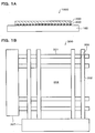
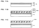
- the lower electrodes 301 function as word lines for selecting rows, and the upper electrodes 302 function as bit lines for selecting columns.
- the lower electrodes 301 and the upper electrodes 302 may be formed so that the lower electrodes 301 function as the word lines and the upper electrodes 302 function as the bit lines.
- the peripheral circuit section 307 has at least a function of writing information in each memory cell of the memory cell array 304 and reading information from each memory cell.
- the peripheral circuit section 307 includes a driver circuit and a signal detection circuit for selectively controlling the lower electrodes 301 and the upper electrodes 302 and the like.
- a Y gate, sense amplifier, input/output buffer, X address decoder, Y address decoder, address buffer, and the like can be given.
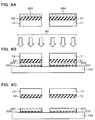
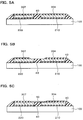
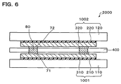
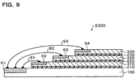
- the sheet-shaped devices 310 and 320 are multi-layered together with the flexible substrates 110 and 120, handling capability during the steps can be increased and the degree of integration can be increased by using simple steps. Moreover, according to this manufacturing method, a process which causes a large amount of load to be applied to each section of the device, such as a formation step of an interlayer dielectric or the like, can be omitted when multi-layering the sheet-shaped devices 310 and 320, whereby the sheet-shaped devices 310 and 320 can be multi-layered and integrated while securing the characteristics of the sheet-shaped devices 310 and 320.
Landscapes
- Engineering & Computer Science (AREA)
- Computer Hardware Design (AREA)
- Semiconductor Memories (AREA)
Abstract
Description
- a memory cell array in which a ferroelectric layer is disposed at least in intersecting regions of a plurality of lower electrodes and a plurality of upper electrodes, the lower and upper electrodes being formed in the shape of lines; and
- a peripheral circuit section for the memory cell array.
wherein the sheet-shaped device includes:
wherein the laminates are stacked, and
wherein each of the sheet-shaped devices includes:
wherein each of the sheet-shaped devices includes:
- (A) The above ferroelectric memory and a sheet-shaped operation processing device may be stacked. According to this feature, the degree of integration of an embedded device including a memory device having a novel thin structure and an operation processing device can be increased.
- (B) An insulating substrate having a through-hole may be disposed between the stacked sheet-shaped devices. According to this feature, since the stacked devices are electrically connected through the through-hole formed in the insulating substrate, a mounting area of the device can be reduced and the interconnect length can be reduced, whereby the device can be driven at high speed.
- (C) The insulating substrate may include an interconnect layer on at least one surface of the insulating substrate or inside the insulating substrate. According to this feature, since interconnection between the stacked devices or in each device is achieved through the insulating substrate, the interconnect structure of each device can be simplified.
- (D) The method of manufacturing a ferroelectric memory may further comprise stacking a plurality of laminates including the second substrate and the sheet-shaped device removed from the first substrate. According to this feature, since the sheet-shaped devices are stacked by stacking the laminates including the second substrate, handling capability during manufacturing steps is increased and the degree of integration of the ferroelectric memory can be increased by multi-layering with simplified steps.
- (E) The method of manufacturing a ferroelectric memory may further comprise:
- bonding the sheet-shaped device removed from the first substrate to another sheet-shaped device formed over another first substrate with a separation layer interposed in-between through an adhesive layer, and removing the other first substrate by applying light through one surface of the other first substrate,
Claims (17)
- A ferroelectric memory comprising:wherein the sheet-shaped device includes:a substrate and a sheet-shaped device formed over the substrate through an adhesive layer,a memory cell array in which a ferroelectric layer is disposed at least in intersecting regions of a plurality of lower electrodes and a plurality of upper electrodes, the lower and upper electrodes being formed in the shape of lines; anda peripheral circuit section for the memory cell array.
- A ferroelectric memory comprising:wherein the laminates are stacked, anda plurality of laminates which include substrates and sheet-shaped devices formed over the substrates through adhesive layers, respectively,
wherein each of the sheet-shaped devices includes:a memory cell array in which a ferroelectric layer is disposed at least in intersecting regions of a plurality of lower electrodes and a plurality of upper electrodes, the lower and upper electrodes being formed in the shape of lines; anda peripheral circuit section for the memory cell array. - A ferroelectric memory comprising:wherein each of the sheet-shaped devices includes:a substrate and a plurality of sheet-shaped devices stacked over the substrate through a plurality of adhesive layers,a memory cell array in which a ferroelectric layer is disposed at least in intersecting regions of a plurality of lower electrodes and a plurality of upper electrodes, the lower and upper electrodes being formed in the shape of lines; anda peripheral circuit section for the memory cell array.
- A ferroelectric memory comprising:a sheet-shaped operation processing device; andthe ferroelectric memory as defined in any one of claims 1 to 3 stacked over the sheet-shaped operation processing device.
- The ferroelectric memory as defined in any one of claims 2 to 4,
wherein an insulating substrate having a through-hole is disposed between the stacked sheet-shaped devices. - The ferroelectric memory as defined in claim 5,
wherein the insulating substrate includes an interconnect layer on at least one surface of the insulating substrate or inside the insulating substrate. - A method of manufacturing a ferroelectric memory comprising:forming a separation layer which changes in a property by absorbing light over a light transmissive first substrate;forming a memory cell array, in which a ferroelectric layer is disposed at least in intersecting regions of a plurality of lower electrodes and a plurality of upper electrodes over a predetermined portion of the separation layer, the lower and upper electrodes being formed in the shape of lines;forming a peripheral circuit section for the memory cell array over the separation layer in a portion other than the predetermined portion;bonding a sheet-shaped device including the memory cell array and the peripheral circuit section to a second substrate through at least an adhesive layer; andremoving the sheet-shaped device from the first substrate by applying light to the separation layer through one surface of the first substrate.
- The method of manufacturing a ferroelectric memory as defined in claim 7, further comprising:stacking a plurality of laminates including the second substrate and the sheet-shaped device removed from the first substrate.
- The method of manufacturing a ferroelectric memory as defined in claim 7, further comprising:wherein a plurality of the sheet-shaped devices are stacked over the second substrate by performing this step at least once.bonding the sheet-shaped device removed from the first substrate to another sheet-shaped device formed over another first substrate with a separation layer interposed in-between through an adhesive layer, and removing the other first substrate by applying light through one surface of the other first substrate,
- A method of manufacturing a ferroelectric memory comprising:forming a separation layer which changes in a property by absorbing light over each of a light transmissive first substrate and a light transmissive second substrate;forming a memory cell array, in which a ferroelectric layer is disposed at least in intersecting regions of a plurality of lower electrodes and a plurality of upper electrodes over the separation layer formed over the first substrate, the lower and upper electrodes being formed in the shape of lines;forming a peripheral circuit section for the memory cell array over the separation layer formed over the second substrate;bonding the memory cell array and the peripheral circuit section to a third substrate through at least adhesive layers; andremoving the memory cell array and the peripheral circuit section respectively from the first substrate and the second substrate by applying light to the separation layers through one surface of the first substrate and through one surface of the second substrate.
- The method of manufacturing a ferroelectric memory as defined in claim 10, further comprising:stacking a plurality of laminates including the third substrate and a sheet-shaped device which includes the memory cell array removed from the first substrate and the peripheral circuit section removed from the second substrate.
- The method of manufacturing a ferroelectric memory as defined in any one of claims 7 to 11,
wherein a raw material for the ferroelectric layer of the memory cell array is a mixture of a ferroelectric material and a paraelectric material, and
wherein the ferroelectric layer is formed by crystallizing the mixture. - The method of manufacturing a ferroelectric memory as defined in claim 12, further comprising:annealing the ferroelectric layer after crystallization by applying laser light to the ferroelectric layer.
- A method of manufacturing a ferroelectric memory comprising:forming a first laminate including a memory cell array, in which a ferroelectric layer is disposed at least in intersecting regions of a plurality of lower electrodes and a plurality of upper electrodes over a first substrate having a coefficient of thermal expansion smaller than a coefficient of thermal expansion of a ferroelectric material, the lower and upper electrodes being formed in the shape of lines;subjecting the first laminate to a first heat treatment and subsequent cooling to cause strain in the first laminate, and removing the memory cell array from the first substrate by subjecting the first laminate to a second heat treatment;forming a separation layer which changes in a property by absorbing light over a light transmissive second substrate, and forming a second laminate which includes a peripheral circuit for the memory cell array over the separation layer;bonding the second laminate on the side of the peripheral circuit to a third substrate;removing the peripheral circuit from the second substrate by changing the properties of the separation layer by applying light to the separation layer from the side of the second substrate of the second laminate; andbonding the memory cell array removed from the first substrate to the third substrate.
- The method of manufacturing a ferroelectric memory as defined in claim 14,
wherein the first heat treatment is performed at a temperature lower than a temperature at which strain is generated at least in the first substrate, and
wherein the second heat treatment is performed at a temperature equal to or lower than the temperature of the first heat treatment. - The method of manufacturing a ferroelectric memory as defined in claim 14 or 15,
wherein a paraelectric phase including Si or Ge is mixed in the ferroelectric layer. - The method of manufacturing a ferroelectric memory as defined in any one of claims 14 to 16,
wherein the first substrate includes a silicon substrate.
Applications Claiming Priority (3)
| Application Number | Priority Date | Filing Date | Title |
|---|---|---|---|
| JP2002238014 | 2002-08-19 | ||
| JP2002238014 | 2002-08-19 | ||
| PCT/JP2003/010306 WO2004017410A1 (en) | 2002-08-19 | 2003-08-13 | Ferroelectric memory and its manufacturing method |
Publications (2)
| Publication Number | Publication Date |
|---|---|
| EP1548833A1 true EP1548833A1 (en) | 2005-06-29 |
| EP1548833A4 EP1548833A4 (en) | 2007-03-21 |
Family
ID=31884449
Family Applications (1)
| Application Number | Title | Priority Date | Filing Date |
|---|---|---|---|
| EP03788099A Withdrawn EP1548833A4 (en) | 2002-08-19 | 2003-08-13 | FERROELECTRIC MEMORY AND METHOD FOR MANUFACTURING THE SAME |
Country Status (4)
| Country | Link |
|---|---|
| US (2) | US6917063B2 (en) |
| EP (1) | EP1548833A4 (en) |
| JP (1) | JPWO2004017410A1 (en) |
| WO (1) | WO2004017410A1 (en) |
Cited By (1)
| Publication number | Priority date | Publication date | Assignee | Title |
|---|---|---|---|---|
| EP1946374A4 (en) * | 2005-11-09 | 2014-01-01 | Semiconductor Energy Lab | SEMICONDUCTOR DEVICE AND METHOD FOR MANUFACTURING THE SAME |
Families Citing this family (11)
| Publication number | Priority date | Publication date | Assignee | Title |
|---|---|---|---|---|
| JP2004241632A (en) * | 2003-02-06 | 2004-08-26 | Seiko Epson Corp | Ferroelectric memory and method of manufacturing the same |
| US7057877B2 (en) * | 2003-08-27 | 2006-06-06 | Seiko Epson Corporation | Capacitor, method of manufacture thereof and semiconductor device |
| JP2005136071A (en) * | 2003-10-29 | 2005-05-26 | Seiko Epson Corp | Cross-point type ferroelectric memory |
| JP4653426B2 (en) | 2004-06-25 | 2011-03-16 | セイコーエプソン株式会社 | Semiconductor device |
| NO20052904L (en) * | 2005-06-14 | 2006-12-15 | Thin Film Electronics Asa | A non-volatile electrical memory system |
| JP4433200B2 (en) * | 2005-12-20 | 2010-03-17 | セイコーエプソン株式会社 | Ferroelectric capacitor and semiconductor device |
| KR20090103113A (en) * | 2008-03-27 | 2009-10-01 | 삼성전자주식회사 | Semiconductor device and method of manufacturing the same |
| US8455936B2 (en) * | 2010-02-25 | 2013-06-04 | Avago Technologies General Ip (Singapore) Pte. Ltd. | Configurable memory sheet and package assembly |
| US8987787B2 (en) * | 2012-04-10 | 2015-03-24 | Macronix International Co., Ltd. | Semiconductor structure and method for manufacturing the same |
| EP3123507A4 (en) * | 2014-03-27 | 2017-12-06 | Intel Corporation | Multi-device flexible electronics system on a chip (soc) process integration |
| JP7688550B2 (en) * | 2021-09-17 | 2025-06-04 | キオクシア株式会社 | Semiconductor device, semiconductor device manufacturing method, and substrate reuse method |
Family Cites Families (12)
| Publication number | Priority date | Publication date | Assignee | Title |
|---|---|---|---|---|
| JP2788265B2 (en) * | 1988-07-08 | 1998-08-20 | オリンパス光学工業株式会社 | Ferroelectric memory, driving method and manufacturing method thereof |
| JPH07202052A (en) * | 1993-12-28 | 1995-08-04 | Hitachi Ltd | Method for manufacturing semiconductor integrated circuit device |
| JP3809712B2 (en) | 1996-08-27 | 2006-08-16 | セイコーエプソン株式会社 | Thin film device transfer method |
| JP4085459B2 (en) | 1998-03-02 | 2008-05-14 | セイコーエプソン株式会社 | Manufacturing method of three-dimensional device |
| JP3690135B2 (en) * | 1998-09-10 | 2005-08-31 | セイコーエプソン株式会社 | Device manufacturing method |
| US6249014B1 (en) * | 1998-10-01 | 2001-06-19 | Ramtron International Corporation | Hydrogen barrier encapsulation techniques for the control of hydrogen induced degradation of ferroelectric capacitors in conjunction with multilevel metal processing for non-volatile integrated circuit memory devices |
| WO2000038234A1 (en) * | 1998-12-04 | 2000-06-29 | Thin Film Electronics Asa | Scalable data processing apparatus |
| US6114088A (en) * | 1999-01-15 | 2000-09-05 | 3M Innovative Properties Company | Thermal transfer element for forming multilayer devices |
| JP3620041B2 (en) * | 1999-12-09 | 2005-02-16 | セイコーエプソン株式会社 | MEMORY DEVICE, ITS MANUFACTURING METHOD, AND ELECTRONIC DEVICE |
| JP2002026282A (en) * | 2000-06-30 | 2002-01-25 | Seiko Epson Corp | Method for manufacturing simple matrix memory device |
| JP2002269972A (en) * | 2000-12-27 | 2002-09-20 | Seiko Epson Corp | Ferroelectric memory device and method of operating memory cell comprising ferroelectric capacitor |
| JP2002217391A (en) * | 2001-01-23 | 2002-08-02 | Seiko Epson Corp | Laminated body manufacturing method and semiconductor device |
-
2003
- 2003-08-13 JP JP2004528873A patent/JPWO2004017410A1/en not_active Withdrawn
- 2003-08-13 WO PCT/JP2003/010306 patent/WO2004017410A1/en not_active Ceased
- 2003-08-13 EP EP03788099A patent/EP1548833A4/en not_active Withdrawn
- 2003-08-14 US US10/640,264 patent/US6917063B2/en not_active Expired - Fee Related
-
2005
- 2005-06-08 US US11/147,279 patent/US20050263809A1/en not_active Abandoned
Cited By (1)
| Publication number | Priority date | Publication date | Assignee | Title |
|---|---|---|---|---|
| EP1946374A4 (en) * | 2005-11-09 | 2014-01-01 | Semiconductor Energy Lab | SEMICONDUCTOR DEVICE AND METHOD FOR MANUFACTURING THE SAME |
Also Published As
| Publication number | Publication date |
|---|---|
| EP1548833A4 (en) | 2007-03-21 |
| US20040232458A1 (en) | 2004-11-25 |
| WO2004017410A1 (en) | 2004-02-26 |
| US20050263809A1 (en) | 2005-12-01 |
| JPWO2004017410A1 (en) | 2005-12-08 |
| US6917063B2 (en) | 2005-07-12 |
Similar Documents
| Publication | Publication Date | Title |
|---|---|---|
| JP4063082B2 (en) | Flexible electronic device and manufacturing method thereof | |
| JP4042182B2 (en) | IC card manufacturing method and thin film integrated circuit device manufacturing method | |
| US10672821B2 (en) | Sensor device and manufacturing method thereof | |
| US6814832B2 (en) | Method for transferring element, method for producing element, integrated circuit, circuit board, electro-optical device, IC card, and electronic appliance | |
| US6917063B2 (en) | Ferroelectric memory and method of fabricating the same | |
| US6700631B1 (en) | Method of separating thin-film device, method of transferring thin-film device, thin-film device, active matrix substrate, and liquid crystal display device | |
| JP2005311205A (en) | Semiconductor device | |
| JP4103421B2 (en) | Electronic device and electronic equipment | |
| JPH11251518A (en) | 3D device | |
| KR20090083362A (en) | Semiconductor device and manufacturing method thereof | |
| JP2003142666A (en) | Element transfer method, element manufacturing method, integrated circuit, circuit board, electro-optical device, IC card, and electronic equipment | |
| JPH10125930A (en) | Peeling method | |
| JP2002217391A (en) | Laminated body manufacturing method and semiconductor device | |
| JP2004172478A (en) | Semiconductor device, method of manufacturing the same, and measuring jig according to the semiconductor device | |
| JP4061846B2 (en) | Laminated body manufacturing method and semiconductor device manufacturing method | |
| US20060166378A1 (en) | Method of producing semiconductor device | |
| JPH10177187A (en) | Method for establishing electrical continuity between transferred thin film structural blocks, method for manufacturing active matrix substrate, active matrix substrate, and liquid crystal device | |
| CN100456476C (en) | Ferroelectric memory and manufacturing method thereof | |
| JP2004296681A (en) | A ferroelectric film, the strength method for producing a dielectric film, strong preparation and ferroelectric memory ferroelectric capacitor and a ferroelectric capacitor | |
| JP5245029B2 (en) | Semiconductor device | |
| JP2023179298A (en) | Semiconductor device and its manufacturing method | |
| JP2004241632A5 (en) | ||
| JP2006245185A (en) | Organic ferroelectric memory and manufacturing method thereof | |
| JP2006253295A (en) | Organic ferroelectric memory and manufacturing method thereof | |
| WO1992002045A1 (en) | Method for manufacturing semiconductor device |
Legal Events
| Date | Code | Title | Description |
|---|---|---|---|
| PUAI | Public reference made under article 153(3) epc to a published international application that has entered the european phase |
Free format text: ORIGINAL CODE: 0009012 |
|
| 17P | Request for examination filed |
Effective date: 20050207 |
|
| AK | Designated contracting states |
Kind code of ref document: A1 Designated state(s): AT BE BG CH CY CZ DE DK EE ES FI FR GB GR HU IE IT LI LU MC NL PT RO SE SI SK TR |
|
| AX | Request for extension of the european patent |
Extension state: AL LT LV MK |
|
| DAX | Request for extension of the european patent (deleted) | ||
| RBV | Designated contracting states (corrected) |
Designated state(s): DE GB |
|
| A4 | Supplementary search report drawn up and despatched |
Effective date: 20070215 |
|
| RIC1 | Information provided on ipc code assigned before grant |
Ipc: H01L 27/115 20060101ALN20070209BHEP Ipc: H01L 27/105 20060101ALN20070209BHEP Ipc: H01L 27/12 20060101ALI20070209BHEP Ipc: H01L 21/84 20060101ALI20070209BHEP Ipc: H01L 21/68 20060101ALI20070209BHEP Ipc: H01L 21/98 20060101ALI20070209BHEP Ipc: H01L 23/48 20060101ALI20070209BHEP Ipc: H01L 25/065 20060101AFI20070209BHEP |
|
| 17Q | First examination report despatched |
Effective date: 20070503 |
|
| STAA | Information on the status of an ep patent application or granted ep patent |
Free format text: STATUS: THE APPLICATION IS DEEMED TO BE WITHDRAWN |
|
| 18D | Application deemed to be withdrawn |
Effective date: 20090526 |