EP1545075A1 - Verfahren und System zur nahtlosen Doppelumschaltung in einer Steuerung für Portumgehung - Google Patents
Verfahren und System zur nahtlosen Doppelumschaltung in einer Steuerung für Portumgehung Download PDFInfo
- Publication number
- EP1545075A1 EP1545075A1 EP04028592A EP04028592A EP1545075A1 EP 1545075 A1 EP1545075 A1 EP 1545075A1 EP 04028592 A EP04028592 A EP 04028592A EP 04028592 A EP04028592 A EP 04028592A EP 1545075 A1 EP1545075 A1 EP 1545075A1
- Authority
- EP
- European Patent Office
- Prior art keywords
- port
- input signal
- bypass
- received input
- block
- Prior art date
- Legal status (The legal status is an assumption and is not a legal conclusion. Google has not performed a legal analysis and makes no representation as to the accuracy of the status listed.)
- Granted
Links
- 238000000034 method Methods 0.000 title claims description 28
- 230000009977 dual effect Effects 0.000 title description 35
- 238000004590 computer program Methods 0.000 claims description 6
- 238000004891 communication Methods 0.000 description 34
- 238000013500 data storage Methods 0.000 description 34
- 238000010586 diagram Methods 0.000 description 28
- 239000000835 fiber Substances 0.000 description 20
- 230000006855 networking Effects 0.000 description 19
- 230000006870 function Effects 0.000 description 12
- 238000005516 engineering process Methods 0.000 description 10
- 238000012545 processing Methods 0.000 description 8
- 238000012360 testing method Methods 0.000 description 7
- 238000001514 detection method Methods 0.000 description 6
- 230000008878 coupling Effects 0.000 description 5
- 238000010168 coupling process Methods 0.000 description 5
- 238000005859 coupling reaction Methods 0.000 description 5
- 230000000977 initiatory effect Effects 0.000 description 5
- 230000003287 optical effect Effects 0.000 description 5
- 230000001934 delay Effects 0.000 description 3
- 238000003491 array Methods 0.000 description 2
- 230000008901 benefit Effects 0.000 description 2
- 230000000694 effects Effects 0.000 description 2
- 239000004744 fabric Substances 0.000 description 2
- 238000011016 integrity testing Methods 0.000 description 2
- 239000000463 material Substances 0.000 description 2
- 238000013459 approach Methods 0.000 description 1
- 230000005540 biological transmission Effects 0.000 description 1
- 230000015556 catabolic process Effects 0.000 description 1
- 230000008859 change Effects 0.000 description 1
- 238000006243 chemical reaction Methods 0.000 description 1
- 238000006731 degradation reaction Methods 0.000 description 1
- 238000010348 incorporation Methods 0.000 description 1
- 230000010365 information processing Effects 0.000 description 1
- 230000010354 integration Effects 0.000 description 1
- 238000012423 maintenance Methods 0.000 description 1
- 238000012986 modification Methods 0.000 description 1
- 230000004048 modification Effects 0.000 description 1
- 238000012544 monitoring process Methods 0.000 description 1
- 230000000135 prohibitive effect Effects 0.000 description 1
- 238000011084 recovery Methods 0.000 description 1
- 230000001360 synchronised effect Effects 0.000 description 1
- 230000033772 system development Effects 0.000 description 1
Images






Classifications
-
- H—ELECTRICITY
- H04—ELECTRIC COMMUNICATION TECHNIQUE
- H04L—TRANSMISSION OF DIGITAL INFORMATION, e.g. TELEGRAPHIC COMMUNICATION
- H04L12/00—Data switching networks
- H04L12/28—Data switching networks characterised by path configuration, e.g. LAN [Local Area Networks] or WAN [Wide Area Networks]
- H04L12/42—Loop networks
- H04L12/437—Ring fault isolation or reconfiguration
-
- H—ELECTRICITY
- H04—ELECTRIC COMMUNICATION TECHNIQUE
- H04L—TRANSMISSION OF DIGITAL INFORMATION, e.g. TELEGRAPHIC COMMUNICATION
- H04L49/00—Packet switching elements
- H04L49/35—Switches specially adapted for specific applications
- H04L49/356—Switches specially adapted for specific applications for storage area networks
- H04L49/357—Fibre channel switches
-
- H—ELECTRICITY
- H04—ELECTRIC COMMUNICATION TECHNIQUE
- H04L—TRANSMISSION OF DIGITAL INFORMATION, e.g. TELEGRAPHIC COMMUNICATION
- H04L49/00—Packet switching elements
- H04L49/55—Prevention, detection or correction of errors
- H04L49/552—Prevention, detection or correction of errors by ensuring the integrity of packets received through redundant connections
Definitions
- Certain embodiments of the invention relate to port bypass controllers. More specifically, certain embodiments of the invention relate to a method and system for seamless dual switching in a port bypass controller.
- FIG. 1 a is a block diagram 120 of a conventional networking environment illustrating the arrangements of various communication and storage entities.
- a wide area network (WAN) 110 comprising a plurality of local area networks (LANs) 102, 104, 106, 108 and a router 132.
- the LANs 102, 104, 106, 108 are coupled via the router 132.
- the LAN 102 comprises PCs 112, 116, 120, servers 126, 128 and data storage elements 114, 118, 122, 124 and 130.
- the data storage element 114 may be coupled to the PC 112, the data storage element 118 may be coupled to the PC 116 and the data storage element 122 may be coupled to the PC 120.
- the data storage element 124 may be coupled to the server 126 and the data storage element 130 may be coupled to the server 128.
- the LANs 104, 106, 108 may also comprise a plurality of PCs, data storage elements and servers which may be configured in a somewhat similar manner as in LAN 102.
- the PCs 112, 116, 120 may communicate with each other and with the servers 126, 128 via the LAN 102.
- the PCs 112, 116, 120 may communicate with communication entities coupled to the LANs 104, 106, 108 via the router 132. Additionally, the communication entities coupled to the LANs 104, 106, 108 may also communicate with the PCs 112, 116, 120, servers 126, 128, and the data storage elements 114, 118, 122, 124, 130 via the router 132.
- a major drawback with the configuration of the conventional networking environment of FIG. 1a is that the bandwidth of the PC's connection or link to the LAN and the server's connection or link to the LAN may severely affect the performance of a communication network. Furthermore, the processing bandwidth of the PC's and the servers may further decrease system performance by introducing delays, which results in increased system latency. For example, it may be desirable for PC 112 to communicate with PC 120 in order to acquire information from the data storage element 122. Accordingly, if the network connections coupling the PC 112 and the PC 120 are slow, then these connections will limit communication between PC 112 and PC 120. Performance of the communication between PC 112 and PC 120 may be further limited or degraded in cases where the processing bandwidth for the PC 112 and PC 120 are low.
- multiple PCs may be attempting to communicate with the PC 120 in order to acquire information from the data storage element 120 while the PC 112 is simultaneously communicating with the PC 120.
- the limited processing bandwidth and communication bandwidth of the PC 112 and the PC 120 may result in further delays and increased latency.
- the PCs 112, 116, 120 therefore, become bottlenecks.
- PC 120 may be desirable for PC 120 to communicate with server 126 in order to acquire information from the data storage element 124. Accordingly, if the network connections coupling the PC 120 and the server 126 are slow, then these connections will limit communication between PC 120 and server 126. Performance of the communication between PC 120 and server 126 may be further limited or degraded in cases where the processing bandwidth for the PC 120 and server 126 are low. Furthermore, during operation, multiple PCs such as PCs 112, 116 may be attempting to communicate with the server 126 in order to acquire information from the data storage element 124, while the PC 120 is simultaneously communicating with the server 126.
- PCs 112, 116 may be attempting to communicate with the server 126 in order to acquire information from the data storage element 124, while the PC 120 is simultaneously communicating with the server 126.
- the limited processing bandwidth and communication bandwidth of the PC 120 and the server 126 may result in further delays and increased latency.
- the bandwidth of the connections of the PCs and servers to the LAN may be increased by adding higher bandwidth connections, this can be a costly venture.
- the processing bandwidth may also be increased by adding faster processors but the cost may be prohibitive.
- FIG. 1b is a block diagram 130 of an improved conventional networking environment illustrating the arrangements of various communication and storage entities, which addresses some of the drawbacks of the networking environment of FIG. 1 a.
- a wide area network (WAN) 110 comprising a plurality of local area networks (LANs) 102, 104, 106, 108 and a router 132.
- the LANs 102, 104, 106, 108 are coupled via the router 132.
- the LAN 102 comprises PCs 112, 116, 120, servers 126, 128 and data storage elements 132 and 134.
- the data storage element 134 may comprise a plurality of storage devices such as a disk array, which may be coupled to the server 126.
- the data storage element 136 may also comprise a plurality of storage devices such as a disk array, which may be coupled to the server 128.
- the LANs 104, 106, 108 may also comprise a plurality of PCs, data storage elements and servers which may be configured in a somewhat similar manner as in LAN 102.
- the PCs 112, 116, 120 may communicate with each other and with the servers 126, 128 via the LAN 102.
- the PCs 112, 116, 120 may also communicate with communication entities coupled to the LANs 104, 106, 108 via the router 132. Additionally, the communication entities coupled to the LANs 104, 106, 108 may also communicate with the PCs 112, 116, 120, servers 126, 128, and the data storage elements 134, 136.
- the servers 126, 128 may be configured so that they have much greater communication and processing bandwidth that the PCs 112, 116, 120. Notwithstanding, although the networking environment configuration of FIG. 1 b may provide better performance than the networking environment of FIG. 1 a, one drawback with the configuration of FIG. 1 b is that the servers 126, 128 are now bottlenecks. In this regard, as the number of connections to the servers requesting information from the data storage entities 134, 136 increases, the servers themselves will become bottlenecks resulting is degradation of system performance.
- FIG. 1c is a block diagram 140 of an improved conventional networking environment illustrating the arrangements of various communication and storage entities, which addresses some of the drawbacks of the networking environment of FIG. 1 a and FIG. 1 b.
- a wide area network (WAN) 110 comprising a plurality of local area networks (LANs) 102, 104, 106, 108, a router 132 and a storage area network (SAN) 142.
- the LANs 102, 104, 106, 108 are coupled via the router 132.
- the LAN 102 comprises PCs 112, 116, 120 and servers 126, 128.
- the storage area network 142 comprises data storage elements 144, 146 and 148.
- the data storage elements 144, 146, 148 may comprise a plurality of storage devices such as disk arrays, which may be coupled to the servers 126, 128 via the storage access network 142.
- Each of the LANs 104, 106, 108 may also comprise a plurality of PCs and servers which may be configured in a somewhat similar manner as in LAN 102.
- One or more servers coupled to the LANs 104, 106, 108 may also be coupled to the storage area network 142 or may communicate with data storage elements 144, 146, 148 via the storage area network 148.
- any of the LANs 102, 104, 106, 108 may communicate directly or indirectly with the storage area network 142, information stored in the data storage elements 144, 146, 148 may be more readily accessible without encountering the bottlenecks previously associated with the networking environments of FIG. 1 a and FIG. 1 b.
- FIG. 2 is a block diagram of an exemplary local area network (LAN) coupled to a storage area network (SAN).
- LANs 202, 204, 206, 208 and storage access network (SAN) 240 may comprise PCs 210, 212, 214, and servers 216, 218.
- the storage area network 240 may comprise a fibre channel (FC) switch 224, file servers (FSs) 226, 228, 230 and a plurality of data storage elements 232, 234, 236.
- Each of the data storage elements 232, 234, 236 may comprise a plurality of fibre channel hard disks.
- the storage access network 240 may be coupled to the LAN 202 via host bus adapters (HBAs) 220, 222, which interfaces with the servers.
- HBAs host bus adapters
- the host bus adapter 220 may be configured to interface with the fibre channel switch 224 and the server 216
- the host bus adapter 222 may be configured to interface with the fibre channel switch 224 and the server 218.
- the file server 226 may be coupled to the data storage element 232
- the file server 228 may be coupled to the data storage element 234
- the file server 230 may be coupled to the data storage element 236.
- the file servers 216, 218 may comprise a plurality of ports to which a data storage device such as a hard disk may be coupled. Each of the file server's plurality of ports may be electrically and/or optically coupled to a single storage element such as a hard disk. In this regard, each of the file servers 226, 228, 230 supports a single point-to-point connection with a particular hard disk.
- the fibre channel switch 224 may be adapted to switch connections between servers and the file servers.
- the fibre channel switch 224 may be adapted to switch connections from the server 216 to any of the file servers 226, 228, 230 in order to provide access to the data storage elements 232, 234, 236 respectively.
- the fibre channel switch 224 may be adapted to switch connections from the server 216 to any of the file servers 226, 228, 230 in order to provide access to any one or more of the data storage elements 232, 234, 236 respectively.
- PC 214 may utilize any of the servers 216, 218 to retrieve information from any of the file servers 232, 234, 236.
- the fibre channel switch 224 may switch the connection from the server 216 to the file server 236.
- a communication device coupled to LAN 204 may establish a connection with server 218 in order to retrieve information from the file server 234.
- the fibre channel switch 224 may switch the connection from the server 218 to the file server 234.
- FIG. 2 provides significantly increased performance over the conventional networking environments illustrated in FIG. 1 a, FIG. 1 b and FIG. 1 c
- a major drawback with the networking environment of FIG. 2 is its point-to-point communication link existing between each of the hard disks and each of the plurality of file server ports.
- the point-to-point communication links existing between each of the hard disks and the file server ports can be quite expensive to operate and/or maintain.
- FC fibre channel
- FIG. 3 is a block diagram of a conventional fibre channel arbitrated loop arrangement which may be utilized for coupling a plurality of hard disks which may be found in the data storage entities of FIG. 1a, FIG. 1b, FIG. 1c and FIG. 2.
- a server 302 a host bus adapter 304, and a plurality of hard disks, namely, 306a, 306b, 306c, 306d, 306e, 306f, 306g, 306h, 306i, 306j and 306k.
- Each of the hard disks 306a, ..., 306k may comprise a port bypass controller and repeater (PBC/R) block.
- PBC/R port bypass controller and repeater
- Each of the port bypass controller and repeater blocks may comprise a dual port architecture for redundancy.
- the host bus adapter 304 interfaces with the server 302 and couples the hard disks to the server 302.
- the hard disks 306a, ..., 306k are arranged in a loop or ring configuration with the first hard disk 306a in the ring coupled to the host bus adapter 304.
- the second hard disk 306b is coupled to the first hard disk 306b and the third hard disk 306c is coupled to the second hard disk 306b.
- the remaining hard disks are coupled or chained in a similar arrangement with the last hard disk 306k in the chain or loop being coupled to the host bus adapter 304.
- the last hard disk 306k is also chained to hard disk 306j.
- the fibre channel arbitrated loop (FC-AL) arrangement is a ring arrangement that is somewhat similar in arrangement to a token ring configuration, but only with regard to their configuration. With regard to its operation, the fibre channel arbitrated loop does not utilize a token for facilitating communication between nodes on the loop. Rather, the fibre channel arbitrated loop utilizes an arbitrated loop address to facilitate communication between the nodes that are coupled to the loop.
- Each of the hard disks that are on the fibre channel arbitrated loop which may also be referred to as a ring, share the bandwidth allocated for the loop.
- Communication over the loop occurs on a point-to-point basis between an initiating hard disk and a destination hard disk.
- the two ports that are active include the port that won loop arbitration and the port that is in communication that won the arbitration.
- the port that has won the arbitration may be referred to as the initiating port and the port in communication with the port that won the arbitration may be referred to as the destination port. Traffic does not have to be routed between the initiating port and destination port since there is point-to-point communication between the initiating port and the destination port.
- ports other than the initiating port and the destination port in the loop are adapted to receive frames and forward the received frames to successive ports in the loop.
- the received frames may be data frames and control frames such as acknowledgements and ready frames.
- a major drawback with this type of receive and forward scheme is the increased latency penalty introduced and incurred by each successive port in the loop.
- Some fibre channel arbitrated loop implementations such as the implementation illustrated in FIG. 3 were based on analog port bypass controller (PBC) and repeaters (R).
- PBC analog port bypass controller
- R repeaters
- the combination of loop architecture with the port bypass controller were prone to problems which often resulted in catastrophic loop failures since one hard disk could potentially affect the operation of all the other hard disks in the loop.
- These port bypass controller implementations required operators or service technicians to insert and/or remove each hard disk individually in order to determine and/or isolate the actual location of a loop failure or failed hard disk. Furthermore, an overwhelming majority of these failures were signal integrity related.
- Certain embodiments of the invention may be found in a method and system for seamless dual switching in a port bypass controller.
- Aspects of the method for seamless port bypass controller operation may comprise receiving an input signal at a first port of a port bypass controller and selecting at least a second port coupled in a chain to the first port. At least a portion of the received input signal may be switched from the first port to at least the second port without initializing or reconfiguring the second port.
- the method may also comprise repeating at least a portion of the received input signal to a second port without initializing or reconfiguring the second port.
- a retimed signal corresponding to at least a portion of the received input signal may be generated and switched to at least the second port without initializing or reconfiguring the second port.
- Timing data may be acquired from the received input signal and at least a transmit path of the second port may be driven by at least a portion of the timing data acquired from the received input signal. At least one port may be bypassed and at least a portion of the received input signal may be switched from the first port to at least a third port coupled in the chain without initializing or reconfiguring the third port. At least a portion of the received input signal may be loopbacked from the first port to at least the second port.
- a retimed signal corresponding to at least a portion of the received input signal may be simultaneously generated for the second port while repeating at least a portion of the received input signal to a third port coupled in the chain without initializing or reconfiguring the second port and/or the third port.
- the method may further comprise bypassing all ports for a first FC-Core coupled in the chain and switching at least a portion of the received input signal to at least one port in a second FC-Core coupled in the chain.
- a rate of the received input signal may be detected and alignment may be made to the word boundaries in the received input signal based on the detected rate of the received input signal.
- Another embodiment of the invention may provide a machine-readable storage, having stored thereon, a computer program having at least one code section executable by a machine, thereby causing the machine to perform the steps as described above for seamless port bypass controller operation.
- aspects of the system for seamless port bypass controller operation may comprise a first port of a port bypass controller that receives an input signal and at least one of a plurality of selectors that selects at least a second port coupled in a chain to the first port. At least one of the selectors may switch at least a portion of the received input signal from the first port to the second port without initializing or reconfiguring at least the second port.
- a repeater may repeat at least a portion of the received input signal to at least the second port without initializing or reconfiguring the second port.
- a retimer may generate a retimed signal corresponding to at least a portion of the received input signal to the second port without initializing or reconfiguring the second port.
- a CDR and/or an interpolator may be configured to acquire timing data from the received input signal and utilize at least a portion of the acquired timing data to drive at least a transmit path of the second port.
- the system may further comprise a bypass selector that may be utilized to bypass at least one port in the chain.
- the bypass selector may be adapted to switch at least a portion of the received input signal from the first port to at least a third port coupled in the chain without initializing or reconfiguring the third port.
- the bypass selector may also be adapted to bypass all ports for a first FC-Core coupled in the chain and switch at least a portion of the received input signal to at least one port in a second FC-Core coupled in the chain.
- a loopback selector may loopback at least a portion of the received input signal from the first port to at least the second port.
- a retimer may simultaneously generate a retimed signal corresponding to at least a portion of the received input signal for the second port while a repeater repeats at least a portion of the received input signal to a third port coupled in the chain without initializing or reconfiguring the second port and/or the third port.
- the system may further comprise a speed detector and a word synchronizer.
- the speed detector may detect a rate of the received input signal and the a word synchronizer may align to the word boundaries in the received input signal based on the rate of the received input signal detected by the speed detector.
- FIG. 1a is a block diagram of a conventional networking environment illustrating the arrangements of various communication and storage entities.
- FIG. 1 b is a block diagram of an improved conventional networking environment illustrating the arrangements of various communication and storage entities, which addresses some of the drawbacks of the networking environment of FIG. 1a.
- FIG. 1c is a block diagram of an improved conventional networking environment illustrating the arrangements of various communication and storage entities, which addresses some of the drawbacks of the networking environment of FIG. 1a and FIG. 1 b.
- FIG. 2 is a block diagram of an exemplary local area network (LAN) coupled to a storage area network (SAN).
- LAN local area network
- SAN storage area network
- FIG. 3 is a block diagram of a conventional fibre channel arbitrated loop arrangement which may be utilized for coupling a plurality of hard disks which may be found in the data storage entities of FIG. 1 a, FIG. 1 b, FIG. 1 c and FIG. 2.
- FIG. 4a is a block diagram illustrating an exemplary IBOD device that may be utilized in connection with seamless dual switching in a port bypass controller, in accordance with and embodiment of the invention.
- FIG. 4b is a graph illustrating a comparison of just bunch of disk (JBOD), intelligent bunch of disk (IBODTM ), switched bunch of disk (SBOD), and fabric bunch of disk (FBODTM ) that may be utilized in connection with seamless dual switching in a port bypass controller, in accordance with an embodiment of the invention.
- JBOD just bunch of disk
- IBODTM intelligent bunch of disk
- SBOD switched bunch of disk
- FBODTM fabric bunch of disk
- FIG. 5 is a block diagram illustrating an exemplary FC-Core repeater/retimer port switch that may be utilized in connection with the IBOD device of FIG. 4a, for example, for seamless dual switching in a port bypass controller, in accordance with an embodiment of the invention.
- FIG. 6 is a block diagram of an exemplary architecture of an FC-Core repeater port switch for a transmit side and a receive side of the FC-Core repeater/retimer port switch of FIG. 5, for example, which may be utilized in connection with the IBOD device of FIG. 4a, for example, for seamless dual switching in a port bypass controller, in accordance with an embodiment of the invention.
- FIG. 7 is a block diagram of an exemplary embodiment of a retimer port switch architecture that may be utilized in connection with the IBOD device of FIG. 4a, for example, for seamless dual switching in a port bypass controller, in accordance with an embodiment of the invention.
- FIG. 8 is a block diagram of a portion of the retimer port switch architecture of FIG. 7 that may be utilized for handling a single FC-Core which may be utilized in connection with the IBOD device of FIG. 4a, for example, for seamless dual switching in a port bypass controller, in accordance with an embodiment of the invention.
- FIG. 9 is a block diagram of another exemplary embodiment of a retimer port switch architecture that may be utilized in connection with the IBOD device of FIG. 4a, for example, for seamless dual switching in a port bypass controller, in accordance with an embodiment of the invention.
- FIG. 10 is a block diagram of a portion of the retimer port switch architecture of FIG. 9, for example, that may be utilized for handling a single FC-Core which may be utilized in connection with the IBOD device of FIG. 4a, for example, for seamless dual switching in a port bypass controller, in accordance with an embodiment of the invention.
- FIG. 11 is a block diagram illustrating an exemplary dual retimer/repeater application that may be utilized in connection with seamless dual switching in a port bypass controller, in accordance with an embodiment of the invention.
- FIG. 12 is a block diagram illustrating an exemplary 12-port PBC IBOD application that may be utilized in connection with seamless dual switching in a port bypass controller, in accordance with an embodiment of the invention.
- Certain embodiments of the invention for seamless dual switching in a port bypass controller may comprise receiving an input signal at a first port of a port bypass controller and selecting at least a second port coupled in a chain to the first port. At least a portion of the received input signal may be switched from the first port to at least the second port without initializing or reconfiguring the at least the second port.
- the method may also comprise repeating at least a portion of the received input signal to the second port without initializing or reconfiguring the second port.
- a retimed signal corresponding to at least a portion of the received input signal may be generated and switched to the second port without initializing or reconfiguring the second port.
- Timing data may be acquired from the received input signal and at least a transmit path of the second port may be driven by at least a portion of the timing data acquired from the received input signal.
- One or more ports may be bypassed and at least a portion of the received input signal may be switched from the first port to at least a third port coupled in the chain without initializing or reconfiguring the third port.
- At least a portion of the received input signal may be loopbacked from the first port to at least the second port.
- Dual switching refers to repeater port switching, retimer port switching, or simultaneous repeater port switching and retimer port switching.
- Active signal integrity Active-SITM
- Active line integrity Active-LITM
- BER bit error rate
- Active-SI/LI improves system reliability, availability, and serviceability (RAS) from the chip level and may aid in, for example, system development, system integration and testing, and system deployment and startup.
- active-SI/LI provides improved time to market (TTM) and may also aid in identifying and isolating faulty system components or entities in the field. All of this translates to reduced ownership cost and significantly lower maintenance costs.
- active signal integrity (Active-SITM ) and active line integrity (Active-LITM ) technology may be incorporated in each fibre channel (FC) port creating a new class of intelligent port bypass controllers (PBCs) which may be referred to as intelligent bunch of disks (IBODs).
- IBOD devices comprise the intelligence of switches but are nonetheless, transparent to data traffic. Accordingly, this may eliminate any possible protocol interoperability problems that may arise.
- Each IBOD port may operate as full retiming with nominal latency of, for example, 2 to 4 fibre channel (FC) words or in repeating mode with a latency of, for example, less than one ( ⁇ 1 ) FC word.
- any conventional or other backplane may be converted with minimal redesign effort in order to utilize active signal integrity (Active-SITM ) technology and active line integrity (Active-LITM ) technology for improved reliability, availability and serviceability (RAS).
- Active-SITM active signal integrity
- Active-LITM active line integrity
- Active-SI and Active-LI technologies may be incorporated in the exemplary port bypass controllers disclosed herein, the invention is not so limited. Accordingly, aspects of the method and system for seamless dual switching in a port bypass controller may be practiced without utilizing Active-SI and Active LI technologies.
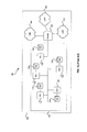
- FIG. 4a is a block diagram illustrating an exemplary IBOD device that may be utilized in connection with seamless dual switching in a port bypass controller, in accordance with and embodiment of the invention.
- the exemplary IBOD device 400 may comprise a plurality of FC-Cores including FC-Core 0 (406), FC-Core 1 (408), and FC-Core 2 (404), a control block 438, a power-up configuration block 440 and a bus interface block 442.
- Each of the FC-Cores 404, 406, 408 has an associated control block which comprises a FC-Core bypass block, a port bypass block, a local loopback block and an EFIFO block.
- the control block for FC-Core 2 (404) comprises FC-Core bypass block 410, port bypass block 412, local loopback block 414 and EFIFO 416.
- the control block for FC-Core 0 (406) comprises FC-Core bypass block 418, port bypass block 420, local loopback block 422 and EFIFO 424.
- the control block for FC-Core 1 (408) comprises FC-Core bypass block 428, port bypass block 430, local loop back block 432 and EFIFO 434.
- the IBOD device 402 may also comprise a bypass and automatic bypass control block 444, speed control block 446, auto bypass control block 448, retimer/repeater control block 450 and loopback control block 452.
- the bypass and automatic bypass control block 444, speed control block 446 and retimer/repeater control block 450 may be coupled to each of the FC-Cores 404, 406, 408.
- the bypass and automatic bypass control block 444 and automatic bypass control block 448 may be coupled to each of the port bypass block 412, 420 and 430.
- the loopback control block 452 may be coupled to each of the local loopback blocks 414, 422, 432 for each of the FC-Cores 404, 406, 408 respectively.
- Each of the FC-Core bypass blocks 410, 718, 428 associated with FC-Cores 404, 406, 408 may comprise a multiplexer or other suitable selector that may be adapted to bypass a corresponding FC-Core when the multiplexer or selector is enabled.
- FC-Core bypass block 410 may be utilized to bypass FC-core 404 when the FC-Core bypass block 410 is enabled.
- the FC-Core bypass block 418 may be utilized to bypass FC-core 406 when the FC-Core bypass block 418 is enabled.
- FC-Core bypass block 428 may be utilized to bypass FC-core 408 when the FC-Core bypass block 428 is enabled. When a FC-Core is bypassed, all the ports for that FC-Core are bypassed.
- Each of the port bypass blocks 412, 420, 430 associated with FC-Cores 404, 406, 408 respectively may comprise suitable logic, circuitry and/or code that may be adapted to effectuate port bypass.
- Each of the local loopback blocks 414, 422, 432 associated with FC-Cores 404, 406, 408 respectively may comprise suitable logic, circuitry and/or code that may be adapted to place a corresponding port of the FC-Core in a local loopback.
- a particular local loopback block may internally configure a particular port of a FC-Core so the transmit (Tx) and receive (Rx) lines for that particular port are cross connected.
- local loopback block 414 may internally configure port 454 of FC-Core 404 so that its transmit (Tx) and receive (Rx) lines are cross connected.
- the loop back control block 452 may comprise suitable logic, circuitry and/or code that may be adapted to control each of the local loopback blocks 414, 422, 432 for each of the FC-Cores 404, 406, 408 respectively.
- loopback control block 452 may configure port 456 associated with FC-Core 406 in a local loopback mode.
- the transmit (Tx) lines and receive (Rx) lines for a particular port may be cross connected from within the corresponding FC-Core.
- Each of the elastic FIFO (EFIFO) blocks 416, 424, 434 associated with FC-Cores 404, 406, 408 respectively may comprise suitable logic and/or circuitry that may be adapted to introduce and change a data rate and/or phase of received and/or transmitted data handled by the FC-Cores 404, 406, 406.
- the bypass and automatic bypass control block 444 and the automatic bypass block 448 may comprise suitable logic, circuitry and/or code that may be adapted to control bypass of at least one of the ports for a particular FC-Core. Accordingly, the bypass and automatic bypass control block 444 and/or the automatic bypass block 448 in conjunction with a corresponding port bypass block may be utilized to bypass one or more of the ports for a particular FC-Core. For example, port bypass and automatic bypass control block 444 and/or the automatic bypass block 448 in conjunction with port bypass block 420 may be configured to enable or disable at least one port such as port 456 of FC-Core 406.
- the speed control block 446 may comprise suitable logic, circuitry and/or code that may be adapted to control and adapt the operation of the FC-Cores 404, 406, 408 to a plurality of different data rates. Additionally, the speed control block may be further adapted for automatic speed negotiation.
- the repeater/retimer block 450 may comprise suitable logic, circuitry and/or code that may be adapted to control retiming and repeating of signals for each of the ports for the FC-Cores integrated within the IBOD device 402.
- the power-up configuration block 440 may comprise suitable logic, circuitry and/or code that may be utilized to initialize the IBOD device 402. Suitable logic may include, but is not limited to, registers and/or memory that may be adapted to store initialization parameters and/or values. For example, the power-up configuration block 440 may comprise a plurality of control registers.
- the control block 438 may comprise suitable logic, circuitry and/or code that may be utilized to configure and control the operations of the IBOD device 402.
- Suitable logic may comprise one or more registers and/or memory that may be adapted to configure various operations for the IBOD device 402.
- the control block 438 may further comprise a plurality of status registers that may be read in order to determine an operational state of the IBOD device.
- the bus interface block 442 may be, for example, a serial or parallel interface bus that may be adapted to provide communication between the IBOD 402 and a host processor or CPU, for example.
- the bus interface block 442 may be a standardized I 2 C bus.
- FIG. 4b is a graph illustrating a comparison of just bunch of disk (JBOD), intelligent bunch of disk (IBODTM ), switched bunch of disk (SBOD), and fabric bunch of disk (FBODTM ) technologies that may be utilized in connection with seamless dual switching in a port bypass controller, in accordance with an embodiment of the invention.
- JBOD just bunch of disk
- IBODTM intelligent bunch of disk
- SBOD switched bunch of disk
- FBODTM fabric bunch of disk
- IBOD One technology driving and enabling IBODs is advanced serializer/deserializer (SerDes or SERDES) technology which incorporates Active-SI and Active-LI.
- SerDes SerDes
- SERDES serializer/deserializer
- FBOD and SBOD have the highest relative cost and greatest complexity
- hybrid implementations of IBOD and FBOD may be provided which offer improved scaling and performance with cost on par with SBOD.
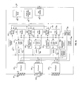
- FIG. 5 is a block diagram illustrating an exemplary FC-Core repeater/retimer port switch that may be utilized in connection with the IBOD device of FIG. 4a, for example, for seamless dual switching in a port bypass controller, in accordance with an embodiment of the invention.
- the FC-Core repeater/retimer port switch may comprise a FC-Core block 512 and a retimer switch block 516.
- the FC-Core block 512 may comprise an active signal integrity block 518, interpolator 520, auto speed detection block 526, word synchronization (WS) block 532, active line integrity block 530, 8B/10B decoder block 528, 8B/10B encoder block 534, and pattern generator 536.
- WS word synchronization
- FIG. 5 further comprises a repeater function block 514 and a retimer function block 516.
- the repeater function block 514 may comprise suitable logic and/or circuitry that may be utilized to implement the repeater function for each FC-Core such as FC-Core 512.
- the repeater function and block 516 illustrates exemplary logic that may be utilized for retiming function.
- the FC-Core repeater/retimer port switch may also comprise a plurality of clock and data recovery (CDR) circuit blocks such as CDRs 524 and 522.
- the CDRs may be arranged in pairs in which a first CDR of a pair is configured to handle a receive (Rx) side and a second CDR of the pair is configured to handle a transmit (Rx) side for a particular port.
- CDR 522 is configured as a receive CDR
- CDR 524 is configured as a transmit CDR.
- the combination of a receive CDR and a transmit CDR pair may be referred to as a port.
- the FC-Core as illustrated comprises four (4) ports.
- each FC-Core may comprise more than or less than four (4) ports.
- Each port may be adapted to handle a single FC hard disk.
- a plurality of FC-ports may be coupled together and integrated into a single chip or integrated circuit.
- three (3) FC-Cores each having four ports may be coupled together and integrated into a single chip which can handle 12 ports.
- a maximum of 12 hard disks may be handled by the twelve (12) ports.
- the interpolator block 520 is illustrated separately from the CDR block 522, the interpolator 520 may be part of the CDR 522. From a functional point of view, as illustrated, the CDR 522 may be viewed as an analog portion and the interpolator 520 may be viewed as a digital portion of a CDR.
- the signal integrity block 518 may be adapted to initiate and manage signal integrity testing.
- the active line integrity block 530 may be adapted to manage line integrity testing.
- United States Application Serial No. (Attorney Docket No. 15366US02) discloses the functions and operation of active signal integrity and active line integrity and is hereby incorporated herein by reference in its entirety.
- the interpolator 520 may be a hardware driven and/or software driven interpolator that may be adapted to track the phase of incoming or received data for active signal integrity operation.
- the auto speed detection block 526 comprises suitable logic, circuitry and/or code that may be adapted to automatically control speed negotiation at the physical coding sublayer (PCS) on the receiver side.
- the auto speed detection block 526 may comprise a firmware algorithm the may reside on-chip within the IBOD device.
- the word synchronization (WS) block 532 may be adapted to provide synchronization at the physical coding sublayer (PCS) on the receiver side.
- the word synchronization (WS) block 532 may be adapted to provide, for example, word boundary alignment.
- the 8B/10B decoder block 528 may be a standardized 8B/10B compliant decoder that may be utilized to decode 10 bits of data into 8 bits of data.
- the 8B/10B encoder block 534 is a standardized 8B/10B compliant encoder that may be utilized to encode 8 bits of data into 10 bits of data.
- the pattern generator 536 may be adapted to generate control words or bit patterns or sequences that may be utilized, for example, for bit error rate testing. In this regard, one or more ports may be placed in loopback and tested by sending, for example, control words, ordered sets and/or bit patterns from the pattern generator 536.
- the auto speed detection block 526 may be adapted to detect the data speed and setup the appropriate clock signals, for example, the transmit and receive clocks, to provide the correct timing.
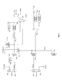
- FIG. 6 is a block diagram of an exemplary architecture of an FC-Core repeater port switch for a transmit side and a receive side of the FC-Core repeater/retimer port switch of FIG. 5, for example, which may be utilized in connection with the IBOD device of FIG. 4a, for example, for seamless dual switching in a port bypass controller, in accordance with an embodiment of the invention.
- FIG. 6 illustrates a transmit side of a first port 602 and a receive side of a second consecutive port 622 of the FC-Core repeater/retimer port switch of FIG. 5. Accordingly, FIG. 6 may be utilized to illustrate the operation of the repeater function block 514 illustrated in FIG. 5.
- the receive side may comprise an active signal integrity (SI) block 634, a selector 606, bypass selector 608, auto speed detection block 612, word synchronizer block 614, active line integrity (LI) block 632, 8B/10B decoder 630, selector 618 and selector 620.
- SI active signal integrity
- LI active line integrity
- Each of the selectors 606, 608, 618 and 620 may comprise suitable logic and/or circuitry that may be adapted to select, enable and/or disable one or more signals that may be coupled thereto. Accordingly, when a signal is received at port 604, the CDR and interpolator (not shown in FIG. 6) may recover the clock and the recovered clock may be utilized to demultiplex the signal. The demultiplexed signal may be passed to the active signal integrity block 634 for processing and/or it may be transferred to the selector 606. This output signal transferred to the selector 606 may be utilized to provide timing for the transmit port Tx(n+1 ) 624.
- the output signal from the selector or MUX 606 may be transferred to the bypass multiplexer or selector 608, and/or the auto speed detection block 612 may determine a data rate of the demultiplexed signal. Once the data rate of the signal has been determined, the resulting timing information may be utilized by the word synchronization (WS) block 614 to align to the word boundaries in the demultiplexed received signal. With regard to port switching, the active line integrity block 632 and the active signal integrity block 634 may not be required.
- a resulting signal from the word synchronization (WS) block 614 may be decoded by the 8B/10B decoder block 630 or it may be processed by the active line integrity block 632.
- the selector or multiplexer 620 may be adapted to select between an output of the word synchronizer block 614 and non-word synchronized version of the demultiplexed received signal.
- the selector or multiplexer 618 may be adapted to select between an output of the 8B/10B decoder and the selector 620.
- a signal received at a current port from a prior port in the chain may be repeated and passed onto a successive port in the chain.
- the CDR for the current receive port may be adapted to recover the clock signal from the signal received from the prior port in the chain. This recovered clock signal may be passed on to a successive port in the chain where it may be utilized to drive the transmit side of the successive port.
- the output signal from the selector or MUX 606 may be transferred to the bypass selector or multiplexer 608 and upon selection by the bypass selector 608, the signal may be repeated to port 632.
- signal 610 from port Rx(n-1) may bypass port 602 and be transferred to ports 624 and/or Tx(n+2).
- the bypass selector or multiplexer 608 may also be referred to as a repeater selector or multiplexer.
- the timing may be acquired from a prior port via signal 610.
- Signal 610 may be derived from, for example, another FC-Core in the chain.
- signal 640 may be passed directly to the selector or multiplexer 632 or signal 640 may be 8B10B encoded by the 8B10B encoder block 626.
- Signal 640 may be a retimed signal, for example.
- the resulting 8B10B encoded signal may be transferred to the selector 632.
- the selector or multiplexer 632 may select either the resulting encoded 8B10 signal or the signal 640 may be transferred to the retransmitter/retimer selector 626.
- the retransmitter/retimer selector 626 may select the output of the selector 632 to be transferred to the transmit port 624.
- the test pattern generator 628 may be utilized for testing and may be configured to generate test codes and/or patterns such as fibre channel codes, frames and/or ordered sets. Accordingly, when utilized in conjunction with port bypass or switching, any port may be readily tested without the need to reconfigure or initialize the port, or to employ expensive external test equipment.
- FIG. 7 is a block diagram of an exemplary embodiment of a retimer port switch architecture that may be utilized in connection with the IBOD device of FIG. 4a, for example, for seamless dual switching in a port bypass controller, in accordance with an embodiment of the invention.
- FIG. 8 is a block diagram of a portion of the retimer port switch architecture of FIG. 7 that may be utilized for handling a single FC-Core which may be utilized in connection with the IBOD device of FIG. 4a, for example, for seamless dual switching in a port bypass controller, in accordance with an embodiment of the invention.
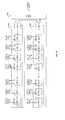
- FC-Core 802 EFIFOs 806, 808, 810, 812 loopback enable selectors or multiplexers 822, 824, 826, 828, bypass selectors 814, 816, 818, 820 and FC-Core bypass enable selector or multiplexer 804.
- FIG. 8 further comprises loopback paths 830, 832, 834 and 836.
- the FC-Core bypass enable selector or multiplexer 804 may be utilized to enable or disable the ports in the FC-Core. For example, if the FC-Core bypass enable selector 804 is enabled, then any of port 0, port 1, port 2 and port 3 may be active. However, if the FC-Core bypass enable selector 804 is disabled, then all of the FC-Core ports including port 0, port 1, port 2 and port 3 will be inactive. In effect, when the FC-Core bypass enable selector 804 is disabled, then the FC-Core 802 is effectively disabled. Notwithstanding, in the case where the FC-Core bypass enable selector 804 is enabled, then any one or more of the of the port for FC-Core 802 may be bypassed.
- bypass enable (be) selector 814 may be utilized to bypass port 0 and bypass enable selector 816 may be utilized to bypass port 1.
- bypass enable selector 818 may be utilized to bypass port 2 and bypass enable selector 820 may be utilized to bypass port 3.
- the loopback enable (Ie) selector 822 may be utilized to place port 0 in loopback via path 830 and the loopback enable selector 824 may be utilized to place port 1 in loopback via path 832.
- the loopback enable selector 826 may be utilized to place port 2 in loopback via path 834 and the loopback enable selector 828 may be utilized to place port 3 in loopback via path 836.
- a signal received from port 3 may pass through EFIFO 812 and be loopbacked through path 836.
- a signal received from port 1 may pass through EFIFO 808 and be loopbacked through path 832.
- FIG. 9 is a block diagram of another exemplary embodiment of a retimer port switch architecture that may be utilized in connection with the IBOD device of FIG. 4a, for example, for seamless dual switching in a port bypass controller, in accordance with an embodiment of the invention.
- FIG. 10 is a block diagram of a portion of the retimer port switch architecture of FIG. 9, for example, that may be utilized for handling a single FC-Core which may be utilized in connection with the IBOD device of FIG. 4a, for example, for seamless dual switching in a port bypass controller, in accordance with an embodiment of the invention.
- FC-Core 1002 EFIFOs 1006, 1008, 1010, 1012, loopback enable selectors or multiplexers 1022, 1024, 1026, 1028, bypass selectors 1014, 1016, 1018, 1020 and FC-Core bypass enable selector or multiplexer 1004.
- EFIFOs 1006, 1008, 1010, 1012 EFIFOs 1006, 1008, 1010, 1012, loopback enable selectors or multiplexers 1022, 1024, 1026, 1028, bypass selectors 1014, 1016, 1018, 1020 and FC-Core bypass enable selector or multiplexer 1004.
- FIG. 10 FC-Core 1002
- the EFIFOs 1006, 1008, 1010, 1012 are configured so that they are located after or at the output of the loopback enable selectors as opposed the FIG. 8 where the EFIFOs 806, 808, 810, 812 are placed before or at the inputs of the bypass selectors 814, 816, 818, 820.
- the FC-Core bypass enable (be) selector or multiplexer 1004 may be utilized to enable or disable the ports in the FC-Core. For example, if the FC-Core bypass enable selector 1004 is enabled, then any of port 0, port 1, port 2 and port 3 may be active. However, if the FC-Core bypass enable selector 1004 is disabled, then all of port 0, port 1, port 2 and port 3 will be inactive. In effect, when the FC-Core bypass enable selector 1004 is disabled, then the FC-Core 1002 is effective disabled. Notwithstanding, in the case where the FC-Core bypass enable selector 1004 is enabled, then any one or more of the ports for FC-Core 1002 may be bypassed.
- bypass enable (be) selector 1014 may be utilized to bypass port 0 and bypass enable selector 1016 may be utilized to bypass port 1.
- bypass enable selector 1018 may be utilized to bypass port 2
- bypass enable selector 1020 may be utilized to bypass port 3.
- the loopback enable (le) selector 1022 may be utilized to place port 0 in loopback via path 1030 and the loopback enable selector 1024 may be utilized to place port 1 in loopback via path 1032.
- the loopback enable selector 1026 may be utilized to place port 2 in loopback via path 1034 and the loopback enable selector 1028 may be utilized to place port 3 in loopback via path 1036.
- a signal received from port 3 may pass through EFIFO 1012 and be loopbacked through path 1036.
- a signal received from port 1 may pass through EFIFO 1008 and be loopbacked through path 1032.
- the retimer signal 1040 may be coupled to any of the ports of the FC-Core 1002 whenever the FC-Core bypass enable selector 1004 is enabled. For example, with the FC-Core bypass enable selector 1004 enabled and the bypass selector 1014 enabled, the retimer signal may be coupled to the EFIFO 1008 for port 2. However, in this case, if the bypass selector 1016 is disabled, then the recovered clock from port 2 will be supplied to port 3.
- FIG. 11 is a block diagram illustrating an exemplary dual retimer/repeater application that may be utilized in connection with seamless dual switching in a port bypass controller, in accordance with an embodiment of the invention.
- a loop card/controller block 1102 a dual retimer/repeater switch block 1104 and a cable/optical interface block 1106.
- the dual retimer/repeater switch block 1104 may comprise a port bypass controller blocks 1108, 1114, repeater/retimer blocks 1110, 1112, active-SI and active-LI block 1116 and bus interface block 1118.
- the loop card controller 1102 may be a CPU or other controller device that may be adapted to handle a plurality of dual retimer/repeater switch blocks, which may be coupled to a backplane bus, for example.
- the cable optical interface 1106 may comprise optical and/or electrical interfaces which may be adapted to provide coupling to a transmission media.
- the port bypass controller 1104 and the repeater/retimer 1110 may be adapted to handle the transmit side from the loop card/controller block 1102 to the cable/optical interface block 1106.
- the port bypass controller 1114 and the repeater/retimer 1112 may be adapted to handle the receive side to the loop card/controller block 1102 from the cable/optical interface block 1106.
- the PBC 1108 on the transmit side may be coupled to the repeater/retimer block 1112 on the receive side to facilitate the repeater and retimer functions.
- clock signals may be recovered from ports on the receive side and utilized to drive ports on the transmit side.
- PBC 1114 on the receive side may be coupled to the repeater/retimer block 1110 on the transmit side to facilitate the repeater and retimer functions.
- clock signals may be recovered from ports on the receive side and utilized to drive ports on the transmit side.
- FIG. 12 is a block diagram illustrating an exemplary 12-port PBC IBOD application that may be utilized in connection with seamless dual switching in a port bypass controller, in accordance with an embodiment of the invention.
- FC-Cores 1202, 1204 and an FC IBOD interface block 1206.
- Each of the FC-Cores 1202, 1204 comprises 12 ports including ports 0-11.
- One port in each of the FC-Cores 1202, 1204 is utilized as an interface port which couples the FC-Cores 1202, 1204 to the FC-IBOD interface block 1206.
- each of the FC-Cores 1202, 1204 may be adapted to handle a maximum of 11 hard disks since one port is utilized for the interface port.
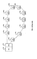
- FIG. 12 also illustrates the daisy chaining of 22 hard disks utilizing two (2) FC-Cores.
- the ports in FC-Core 1202 are chained with PBC0 being the first port and PBC10 in FC-Core 1204 being the last port in the chain.
- PBC10 in FC-Core 1202 is coupled to PBC0 in FC-Core 1204 via the interface PBCs, namely PBC11 of FC-Core 1202 and PBC11 of FC-Core 1204.
- data from the FC IBOD interface 1206 may be transferred to PBC11 of FC-Core 1202, traverse ports PBC0 through PBC10 of FC-Core 1202, pass back through PBC11 of FC-Core 1202 and into PBC11 of FC-Core 1204, traverse PBC10 through PBC0 of FC-Core 1204 and pass back through PBC11 of FC-Core 1204 into the FC IBOD interface 1206.
- dual switching may be provided utilizing, for example, separate retimer and repeater working in unison and this may significantly improve latency for the ports of the FC-Core.
- the retimer may be optimized for maximum flexibility and the repeater may be optimized for low latency.
- Automatic multi-port bypass may also be provided in order to minimizing latency among the ports of the FC-Core.
- the flexible architecture provided by the FC-Core may facilitate the coexistence of a plurality of functions, for example, port bypass, multi-port bypass, loopback and continuous monitoring of incoming signals in a port bypass controller.
- the present invention may be realized in hardware, software, or a combination of hardware and software.
- the present invention may be realized in a centralized fashion in at least one computer system, or in a distributed fashion where different elements are spread across several interconnected computer systems. Any kind of computer system or other apparatus adapted for carrying out the methods described herein is suited.
- a typical combination of hardware and software may be a general-purpose computer system with a computer program that, when being loaded and executed, controls the computer system such that it carries out the methods described herein.
- the present invention may also be embedded in a computer program product, which comprises all the features enabling the implementation of the methods described herein, and which when loaded in a computer system is able to carry out these methods.
- Computer program in the present context means any expression, in any language, code or notation, of a set of instructions intended to cause a system having an information processing capability to perform a particular function either directly or after either or both of the following: a) conversion to another language, code or notation; b) reproduction in a different material form.
Landscapes
- Engineering & Computer Science (AREA)
- Computer Networks & Wireless Communication (AREA)
- Signal Processing (AREA)
- Data Exchanges In Wide-Area Networks (AREA)
- Studio Circuits (AREA)
Applications Claiming Priority (10)
| Application Number | Priority Date | Filing Date | Title |
|---|---|---|---|
| US52942103P | 2003-12-12 | 2003-12-12 | |
| US52914303P | 2003-12-12 | 2003-12-12 | |
| US52914503P | 2003-12-12 | 2003-12-12 | |
| US52920003P | 2003-12-12 | 2003-12-12 | |
| US529421P | 2003-12-12 | ||
| US529145P | 2003-12-12 | ||
| US529200P | 2003-12-12 | ||
| US529143P | 2003-12-12 | ||
| US779234 | 2004-02-13 | ||
| US10/779,234 US8243590B2 (en) | 2003-12-12 | 2004-02-13 | Method and system for seamless dual switching in a port bypass controller |
Publications (2)
| Publication Number | Publication Date |
|---|---|
| EP1545075A1 true EP1545075A1 (de) | 2005-06-22 |
| EP1545075B1 EP1545075B1 (de) | 2011-08-03 |
Family
ID=34528383
Family Applications (1)
| Application Number | Title | Priority Date | Filing Date |
|---|---|---|---|
| EP04028592A Expired - Lifetime EP1545075B1 (de) | 2003-12-12 | 2004-12-02 | Verfahren und System zur nahtlosen Doppelumschaltung in einer Steuerung für Portumgehung |
Country Status (3)
| Country | Link |
|---|---|
| US (1) | US8243590B2 (de) |
| EP (1) | EP1545075B1 (de) |
| TW (1) | TWI264900B (de) |
Families Citing this family (2)
| Publication number | Priority date | Publication date | Assignee | Title |
|---|---|---|---|---|
| CN114691558B (zh) * | 2021-10-20 | 2023-06-20 | 澜起电子科技(上海)有限公司 | 低延迟重定时器及延迟控制方法 |
| WO2023141770A1 (zh) * | 2022-01-25 | 2023-08-03 | 华为技术有限公司 | 中继器的旁路电路及测试方法 |
Citations (5)
| Publication number | Priority date | Publication date | Assignee | Title |
|---|---|---|---|---|
| US6055228A (en) | 1996-12-23 | 2000-04-25 | Lsi Logic Corporation | Methods and apparatus for dynamic topology configuration in a daisy-chained communication environment |
| US20020046276A1 (en) * | 2000-07-06 | 2002-04-18 | Coffey Aedan Diarmuid Cailean | Fibre channel diagnostics in a storage enclosure |
| US20020191537A1 (en) | 2001-06-14 | 2002-12-19 | Nec Corporation | Method and apparatus for diagnosing FC-AL system link |
| US20030031163A1 (en) | 2001-08-06 | 2003-02-13 | Cashman Paul Nicholas | Method and apparatus for improving performance of a loop network |
| US20040062509A1 (en) * | 2002-09-26 | 2004-04-01 | Peeke Douglas E. | Storage system with a diskless enclosure |
Family Cites Families (11)
| Publication number | Priority date | Publication date | Assignee | Title |
|---|---|---|---|---|
| US5524109A (en) * | 1991-06-20 | 1996-06-04 | Bay Networks, Incorporated | Token ring concentrator having retiming function |
| US5991891A (en) * | 1996-12-23 | 1999-11-23 | Lsi Logic Corporation | Method and apparatus for providing loop coherency |
| US5978379A (en) * | 1997-01-23 | 1999-11-02 | Gadzoox Networks, Inc. | Fiber channel learning bridge, learning half bridge, and protocol |
| US6550029B1 (en) * | 1999-10-08 | 2003-04-15 | Emc Corporation | Testing system and methods with protocol pattern injection and external verification |
| US7082100B2 (en) * | 2001-02-28 | 2006-07-25 | Emc Corporation | Storage system adapter and method of using same |
| US7486894B2 (en) * | 2002-06-25 | 2009-02-03 | Finisar Corporation | Transceiver module and integrated circuit with dual eye openers |
| US7664018B2 (en) | 2002-07-02 | 2010-02-16 | Emulex Design & Manufacturing Corporation | Methods and apparatus for switching fibre channel arbitrated loop devices |
| WO2004034641A1 (en) * | 2002-10-09 | 2004-04-22 | Xyratex Technology Limited | Connection apparatus and method for network testers and analysers |
| WO2004056043A1 (en) * | 2002-12-17 | 2004-07-01 | Xyratex Technology Limited | Network tap module |
| US7184395B2 (en) * | 2003-03-18 | 2007-02-27 | Hewlett-Packard Development Company, L.P. | Providing reconditioned signals at a plurality of ports |
| US7451362B2 (en) * | 2003-12-12 | 2008-11-11 | Broadcom Corporation | Method and system for onboard bit error rate (BER) estimation in a port bypass controller |
-
2004
- 2004-02-13 US US10/779,234 patent/US8243590B2/en active Active
- 2004-12-02 EP EP04028592A patent/EP1545075B1/de not_active Expired - Lifetime
- 2004-12-10 TW TW093138403A patent/TWI264900B/zh not_active IP Right Cessation
Patent Citations (5)
| Publication number | Priority date | Publication date | Assignee | Title |
|---|---|---|---|---|
| US6055228A (en) | 1996-12-23 | 2000-04-25 | Lsi Logic Corporation | Methods and apparatus for dynamic topology configuration in a daisy-chained communication environment |
| US20020046276A1 (en) * | 2000-07-06 | 2002-04-18 | Coffey Aedan Diarmuid Cailean | Fibre channel diagnostics in a storage enclosure |
| US20020191537A1 (en) | 2001-06-14 | 2002-12-19 | Nec Corporation | Method and apparatus for diagnosing FC-AL system link |
| US20030031163A1 (en) | 2001-08-06 | 2003-02-13 | Cashman Paul Nicholas | Method and apparatus for improving performance of a loop network |
| US20040062509A1 (en) * | 2002-09-26 | 2004-04-01 | Peeke Douglas E. | Storage system with a diskless enclosure |
Also Published As
| Publication number | Publication date |
|---|---|
| US20050131988A1 (en) | 2005-06-16 |
| TW200531476A (en) | 2005-09-16 |
| TWI264900B (en) | 2006-10-21 |
| US8243590B2 (en) | 2012-08-14 |
| EP1545075B1 (de) | 2011-08-03 |
Similar Documents
| Publication | Publication Date | Title |
|---|---|---|
| US7200108B2 (en) | Method and apparatus for recovery from faults in a loop network | |
| US7451362B2 (en) | Method and system for onboard bit error rate (BER) estimation in a port bypass controller | |
| US9998215B2 (en) | Diagnostic port for inter-switch link testing in electrical, optical and remote loopback modes | |
| JP3738826B2 (ja) | ループにおける自動切離し | |
| EP1480391B1 (de) | Vorrichtung mit physikalischer Schicht mit analoger Serdes-Durchgangsbetriebsart | |
| JP3630739B2 (ja) | ローカルエリア・ネットワークシステムおよびスイッチング方法 | |
| US7110414B2 (en) | Cross-point switch for a fiber channel arbitrated loop | |
| US20050066045A1 (en) | Integrated network interface supporting multiple data transfer protocols | |
| GB2377144A (en) | A method and apparatus for recovery from faults in a loop network by bypassing and selectively un-bypassing ports to ascertain location of fault | |
| US20020046276A1 (en) | Fibre channel diagnostics in a storage enclosure | |
| GB2376612A (en) | Fault location in a loop network | |
| CN113965533A (zh) | 用于数据路径冗余的具有广播和多路复用的有源以太网线缆 | |
| US8594080B2 (en) | Multiple functionality in a virtual storage area network device | |
| US20070183316A1 (en) | Method and Apparatus for Detection of Port Name in a Loop Network | |
| US20070183337A1 (en) | FC-AL cabling management system | |
| US7492783B2 (en) | Method and system for LIPf7 origination detection and LIPf8 suppression in a port bypass controller | |
| KR20010052290A (ko) | 루프 네트워크에서 무효 데이터의 제거 | |
| US20050131987A1 (en) | Method and system for robust elastic FIFO (EFIFO) in a port bypass controller | |
| JP2002514835A (ja) | ジッタ転送のないハブポート | |
| EP2775678B1 (de) | Diagnoseanschluss für Inter-Switch- und Knoten-Linkprüfung in elektrischen, optischen und Fernrückschleifenmodi | |
| US8243590B2 (en) | Method and system for seamless dual switching in a port bypass controller | |
| US7388843B2 (en) | Method and apparatus for testing loop pathway integrity in a fibre channel arbitrated loop | |
| US7443788B2 (en) | Method and apparatus for improving performance of a loop network | |
| CN100531107C (zh) | 在一个端口旁路控制器内进行无缝双转换的方法和系统 | |
| US20060104206A1 (en) | Apparatus, system, and method for detecting a fibre channel miscabling event |
Legal Events
| Date | Code | Title | Description |
|---|---|---|---|
| PUAI | Public reference made under article 153(3) epc to a published international application that has entered the european phase |
Free format text: ORIGINAL CODE: 0009012 |
|
| AK | Designated contracting states |
Kind code of ref document: A1 Designated state(s): AT BE BG CH CY CZ DE DK EE ES FI FR GB GR HU IE IS IT LI LT LU MC NL PL PT RO SE SI SK TR |
|
| AX | Request for extension of the european patent |
Extension state: AL BA HR LV MK YU |
|
| 17P | Request for examination filed |
Effective date: 20051222 |
|
| AKX | Designation fees paid |
Designated state(s): DE FR GB |
|
| 17Q | First examination report despatched |
Effective date: 20060210 |
|
| RAP1 | Party data changed (applicant data changed or rights of an application transferred) |
Owner name: BROADCOM CORPORATION |
|
| GRAP | Despatch of communication of intention to grant a patent |
Free format text: ORIGINAL CODE: EPIDOSNIGR1 |
|
| GRAS | Grant fee paid |
Free format text: ORIGINAL CODE: EPIDOSNIGR3 |
|
| GRAA | (expected) grant |
Free format text: ORIGINAL CODE: 0009210 |
|
| AK | Designated contracting states |
Kind code of ref document: B1 Designated state(s): DE FR GB |
|
| REG | Reference to a national code |
Ref country code: GB Ref legal event code: FG4D |
|
| REG | Reference to a national code |
Ref country code: DE Ref legal event code: R081 Ref document number: 602004033741 Country of ref document: DE Owner name: AVAGO TECHNOLOGIES GENERAL IP (SINGAPORE) PTE., SG Free format text: FORMER OWNER: BROADCOM CORP., IRVINE, CALIF., US |
|
| REG | Reference to a national code |
Ref country code: DE Ref legal event code: R096 Ref document number: 602004033741 Country of ref document: DE Effective date: 20110929 |
|
| PLBE | No opposition filed within time limit |
Free format text: ORIGINAL CODE: 0009261 |
|
| STAA | Information on the status of an ep patent application or granted ep patent |
Free format text: STATUS: NO OPPOSITION FILED WITHIN TIME LIMIT |
|
| 26N | No opposition filed |
Effective date: 20120504 |
|
| REG | Reference to a national code |
Ref country code: DE Ref legal event code: R097 Ref document number: 602004033741 Country of ref document: DE Effective date: 20120504 |
|
| REG | Reference to a national code |
Ref country code: FR Ref legal event code: ST Effective date: 20120831 |
|
| PG25 | Lapsed in a contracting state [announced via postgrant information from national office to epo] |
Ref country code: FR Free format text: LAPSE BECAUSE OF NON-PAYMENT OF DUE FEES Effective date: 20120102 |
|
| PGFP | Annual fee paid to national office [announced via postgrant information from national office to epo] |
Ref country code: GB Payment date: 20151221 Year of fee payment: 12 |
|
| REG | Reference to a national code |
Ref country code: DE Ref legal event code: R082 Ref document number: 602004033741 Country of ref document: DE Representative=s name: BOSCH JEHLE PATENTANWALTSGESELLSCHAFT MBH, DE Ref country code: DE Ref legal event code: R081 Ref document number: 602004033741 Country of ref document: DE Owner name: AVAGO TECHNOLOGIES INTERNATIONAL SALES PTE. LT, SG Free format text: FORMER OWNER: BROADCOM CORP., IRVINE, CALIF., US Ref country code: DE Ref legal event code: R081 Ref document number: 602004033741 Country of ref document: DE Owner name: AVAGO TECHNOLOGIES GENERAL IP (SINGAPORE) PTE., SG Free format text: FORMER OWNER: BROADCOM CORP., IRVINE, CALIF., US |
|
| GBPC | Gb: european patent ceased through non-payment of renewal fee |
Effective date: 20161202 |
|
| REG | Reference to a national code |
Ref country code: GB Ref legal event code: 732E Free format text: REGISTERED BETWEEN 20171005 AND 20171011 |
|
| PG25 | Lapsed in a contracting state [announced via postgrant information from national office to epo] |
Ref country code: GB Free format text: LAPSE BECAUSE OF NON-PAYMENT OF DUE FEES Effective date: 20161202 |
|
| REG | Reference to a national code |
Ref country code: DE Ref legal event code: R082 Ref document number: 602004033741 Country of ref document: DE Representative=s name: BOSCH JEHLE PATENTANWALTSGESELLSCHAFT MBH, DE Ref country code: DE Ref legal event code: R081 Ref document number: 602004033741 Country of ref document: DE Owner name: AVAGO TECHNOLOGIES INTERNATIONAL SALES PTE. LT, SG Free format text: FORMER OWNER: AVAGO TECHNOLOGIES GENERAL IP (SINGAPORE) PTE. LTD., SINGAPORE, SG |
|
| PGFP | Annual fee paid to national office [announced via postgrant information from national office to epo] |
Ref country code: DE Payment date: 20211210 Year of fee payment: 18 |
|
| REG | Reference to a national code |
Ref country code: DE Ref legal event code: R119 Ref document number: 602004033741 Country of ref document: DE |
|
| PG25 | Lapsed in a contracting state [announced via postgrant information from national office to epo] |
Ref country code: DE Free format text: LAPSE BECAUSE OF NON-PAYMENT OF DUE FEES Effective date: 20230701 |