EP1544646A1 - Mach-Zehnder Interferometer, optischer Koppler und Verfahren zu seiner Herstellung - Google Patents
Mach-Zehnder Interferometer, optischer Koppler und Verfahren zu seiner Herstellung Download PDFInfo
- Publication number
- EP1544646A1 EP1544646A1 EP04078456A EP04078456A EP1544646A1 EP 1544646 A1 EP1544646 A1 EP 1544646A1 EP 04078456 A EP04078456 A EP 04078456A EP 04078456 A EP04078456 A EP 04078456A EP 1544646 A1 EP1544646 A1 EP 1544646A1
- Authority
- EP
- European Patent Office
- Prior art keywords
- wave guide
- optical wave
- input optical
- forming
- output
- Prior art date
- Legal status (The legal status is an assumption and is not a legal conclusion. Google has not performed a legal analysis and makes no representation as to the accuracy of the status listed.)
- Withdrawn
Links
- 230000003287 optical effect Effects 0.000 title claims abstract description 543
- 238000004519 manufacturing process Methods 0.000 title claims description 33
- 239000000203 mixture Substances 0.000 claims abstract description 9
- 229910052751 metal Inorganic materials 0.000 claims description 71
- 239000002184 metal Substances 0.000 claims description 71
- 239000000758 substrate Substances 0.000 claims description 69
- RTAQQCXQSZGOHL-UHFFFAOYSA-N Titanium Chemical compound [Ti] RTAQQCXQSZGOHL-UHFFFAOYSA-N 0.000 claims description 28
- 239000013078 crystal Substances 0.000 claims description 28
- 239000010936 titanium Substances 0.000 claims description 28
- 229910052719 titanium Inorganic materials 0.000 claims description 28
- 238000009792 diffusion process Methods 0.000 claims description 13
- 230000000644 propagated effect Effects 0.000 claims description 11
- GQYHUHYESMUTHG-UHFFFAOYSA-N lithium niobate Chemical compound [Li+].[O-][Nb](=O)=O GQYHUHYESMUTHG-UHFFFAOYSA-N 0.000 claims description 6
- 238000010030 laminating Methods 0.000 claims description 3
- 230000000873 masking effect Effects 0.000 claims description 2
- 230000015572 biosynthetic process Effects 0.000 description 37
- 230000008033 biological extinction Effects 0.000 description 22
- 238000002360 preparation method Methods 0.000 description 6
- 230000015556 catabolic process Effects 0.000 description 5
- 238000006731 degradation reaction Methods 0.000 description 5
- 238000005516 engineering process Methods 0.000 description 5
- 239000013307 optical fiber Substances 0.000 description 5
- 230000007261 regionalization Effects 0.000 description 3
- WPYMKLBDIGXBTP-UHFFFAOYSA-N benzoic acid Chemical compound OC(=O)C1=CC=CC=C1 WPYMKLBDIGXBTP-UHFFFAOYSA-N 0.000 description 2
- 238000009826 distribution Methods 0.000 description 2
- 238000000034 method Methods 0.000 description 2
- WSMQKESQZFQMFW-UHFFFAOYSA-N 5-methyl-pyrazole-3-carboxylic acid Chemical compound CC1=CC(C(O)=O)=NN1 WSMQKESQZFQMFW-UHFFFAOYSA-N 0.000 description 1
- 239000005711 Benzoic acid Substances 0.000 description 1
- 238000005452 bending Methods 0.000 description 1
- 235000010233 benzoic acid Nutrition 0.000 description 1
- 230000001419 dependent effect Effects 0.000 description 1
- 239000007788 liquid Substances 0.000 description 1
- 238000012986 modification Methods 0.000 description 1
- 230000004048 modification Effects 0.000 description 1
- 230000001902 propagating effect Effects 0.000 description 1
- 238000006467 substitution reaction Methods 0.000 description 1
- 238000011144 upstream manufacturing Methods 0.000 description 1
Images



Classifications
-
- G—PHYSICS
- G02—OPTICS
- G02B—OPTICAL ELEMENTS, SYSTEMS OR APPARATUS
- G02B6/00—Light guides; Structural details of arrangements comprising light guides and other optical elements, e.g. couplings
- G02B6/10—Light guides; Structural details of arrangements comprising light guides and other optical elements, e.g. couplings of the optical waveguide type
- G02B6/12—Light guides; Structural details of arrangements comprising light guides and other optical elements, e.g. couplings of the optical waveguide type of the integrated circuit kind
- G02B6/13—Integrated optical circuits characterised by the manufacturing method
- G02B6/134—Integrated optical circuits characterised by the manufacturing method by substitution by dopant atoms
- G02B6/1345—Integrated optical circuits characterised by the manufacturing method by substitution by dopant atoms using ion exchange
-
- G—PHYSICS
- G02—OPTICS
- G02B—OPTICAL ELEMENTS, SYSTEMS OR APPARATUS
- G02B6/00—Light guides; Structural details of arrangements comprising light guides and other optical elements, e.g. couplings
- G02B6/10—Light guides; Structural details of arrangements comprising light guides and other optical elements, e.g. couplings of the optical waveguide type
- G02B6/12—Light guides; Structural details of arrangements comprising light guides and other optical elements, e.g. couplings of the optical waveguide type of the integrated circuit kind
- G02B6/122—Basic optical elements, e.g. light-guiding paths
- G02B6/125—Bends, branchings or intersections
-
- G—PHYSICS
- G02—OPTICS
- G02B—OPTICAL ELEMENTS, SYSTEMS OR APPARATUS
- G02B6/00—Light guides; Structural details of arrangements comprising light guides and other optical elements, e.g. couplings
- G02B6/10—Light guides; Structural details of arrangements comprising light guides and other optical elements, e.g. couplings of the optical waveguide type
- G02B6/12—Light guides; Structural details of arrangements comprising light guides and other optical elements, e.g. couplings of the optical waveguide type of the integrated circuit kind
- G02B6/13—Integrated optical circuits characterised by the manufacturing method
- G02B6/134—Integrated optical circuits characterised by the manufacturing method by substitution by dopant atoms
- G02B6/1342—Integrated optical circuits characterised by the manufacturing method by substitution by dopant atoms using diffusion
-
- G—PHYSICS
- G02—OPTICS
- G02B—OPTICAL ELEMENTS, SYSTEMS OR APPARATUS
- G02B6/00—Light guides; Structural details of arrangements comprising light guides and other optical elements, e.g. couplings
- G02B6/10—Light guides; Structural details of arrangements comprising light guides and other optical elements, e.g. couplings of the optical waveguide type
- G02B6/12—Light guides; Structural details of arrangements comprising light guides and other optical elements, e.g. couplings of the optical waveguide type of the integrated circuit kind
- G02B2006/12133—Functions
- G02B2006/12147—Coupler
Definitions
- the present invention relates to a Mach-Zehnder interferometer, an optical coupler, and a manufacturing method of the optical coupler. More particularly, the present invention relates to a Mach-Zehnder interferometer and an optical coupler having a good extinction ratio, and a manufacturing method of the optical coupler.
- an optical coupler including a first optical wave guide which propagates first light, a second optical wave guide which propagates second light, and an output optical wave guide which propagates mixed light, which is the mixture of the first light and the second light, and output it from its one end.
- the luminous intensity output from the output optical wave guide varies due to the interference of the two lights input from the first and second optical wave guides into the output optical wave guide depending on the phase of each light.
- the two lights when the two lights, of which the intensities are the same as each other and the phases are inverted from each other, enter the output optical wave guide, it is preferable that such the lights are offset mutually, emitted from the periphery of the output optical wave guide, and the output luminous intensity is made to be zero.
- an extinction ratio is defined as an index indicating a property of the optical coupler.
- the extinction ratio is a ratio of the output luminous intensity when the two lights, having the same intensities and the reversed phase, enter the output optical wave guide, to the output luminous intensity when the two lights, having the same intensities and the same phases, enter the output optical wave guide.
- Japanese Patent Laid-Open No. 8-194195 discloses some technologies to improve the extinction ratio in the optical coupler.
- Japanese Patent Laid-Open No. 8-194195 discloses a technology which improves the separability of output light and emission light by either means of bending the output optical wave guide, or shifting the optical axes of the first optical wave guide and the second optical wave guide for the Mach-Zehnder light modulator.
- Japanese Patent Laid-Open No. 9-318367 discloses a technology which provides a slot between the first optical wave guide and the second optical wave guide etc. and the output optical wave guide being bent in an optical fiber gyroscope which includes the optical coupler, which improves the separability of the output light and the emission light, and improves the observed extinction ratio.
- Japanese Patent No. 3102874 and Japanese Patent Laid-Open No. 9-21985 disclose a technology for making the width of the incidence wave guide small to reduce the branching ratio variance due to the light incidence with axial shift for a Y-branching optical circuit which propagates the incident light in an incidence wave guide and branches the light to a first wave guide and a second wave guide.
- Japanese Patent Laid-Open No. 10-73792 discloses a technology for the Mach-Zehnder modulator which provides a central taper section between a Mach-Zehnder light modulator for guiding light of high intensity and an optical fiber for guiding light of low intensity to reduce the influence of the shift of the optical axis at the portion where the Mach-Zehnder modulator meets the optical fiber.
- the emission light caused as a result of the interference of the first light and the second light in the optical coupler is separated from the output light of the output optical wave guide so that only the output light can be observed. This prevents observing the emission light even when the lights having the same intensity and inverted phase enter the first optical wave guide and the second optical wave guide, so that the degradation of the extinction ratio can be reduced.
- the space for arranging a third optical waveguide, which is bent, and for providing a slot between the optical wave guides are needed, and consequently that increases a manufacturing cost.
- the inventors of the present application discovered that the extinction ratio deteriorates also according to a cause different from above all, as a result of investigating the causes which degrade the extinction ratio in the optical coupler in order to further improve the extinction ratio of the optical coupler.
- an optical coupler having a Y-branch operable to mix and output a first light and a second light from outside.
- the optical coupler includes: a first input optical wave guide operable to propagate the first light from outside; a second input optical wave guide operable to propagate the second light from outside; an optical coupler operable to output a mixed light, which is a mixture of the first light and the second light; and an output optical wave guide operable to propagate the mixed light and to output it from an end, wherein percentage per unit length of emitting light being propagated in the output optical wave guide to a periphery of the output optical wave guide is higher than that of the first input optical wave guide or the second input optical wave guide.
- a width of the output optical wave guide may be less than a width of the first input optical wave guide or a width of the second input optical wave guide.
- a cross section area of the output optical wave guide may be less than a cross section area of the first input optical wave guide or a cross section area of the second input optical wave guide.
- the first input optical wave guide, the second input optical wave guide, and the output optical wave guide may be formed by diffusing metal into portions where the optical wave guides are to be formed in a substrate made of a ferroelectric crystal, and amount of metal diffusion per unit length of the output optical wave guide may be less than that of the first input optical wave guide or the second input optical wave guide.
- first input optical wave guide, the second input optical wave guide, and the output optical wave guide may be formed by diffusing titanium into portions where the optical wave guides are to be formed in a substrate made of lithium niobate, and amount of titanium diffusion per unit length of the output optical wave guide may be less than that of the first input optical wave guide or the second input optical wave guide.
- the first input optical wave guide, the second input optical wave guide, and the output optical wave guide may be formed by proton exchange of portion where the optical wave guides are to be formed in a substrate made of a ferroelectric crystal, and amount of proton exchange per unit length of the output optical wave guide may be less than that of the first input optical wave guide or the second input optical wave guide.
- a Mach-Zehnder interferometer includes: an optical branch operable to branch an input light; and an optical mixer operable to mix two branched lights, wherein the Mach-Zehnder interferometer employs the optical coupler according to the first aspect of the present invention for the optical mixer.
- the Mach-Zehnder interferometer may further employ the optical coupler according to the first aspect of the present invention for the optical branch.
- a manufacturing method of an optical coupler having a Y-branch operable to mix and output a first light and a second light from outside includes steps of forming a first input optical wave guide operable to propagate the first light from outside; forming a second input optical wave guide operable to propagate the second light from outside; forming an optical coupler operable to output a mixed light, which is a mixture of the first light and the second light; and forming an output optical wave guide operable to propagate the mixed light and to output it from an end, wherein the output optical wave guide is formed in the step of forming an output optical wave guide so that a percentage per unit length of emitting light being propagated therein to a periphery of the output optical wave guide is higher than that of the first input optical wave guide or the second input optical wave guide.
- Each of the step of forming a first input optical wave guide, the step of forming a second input optical wave guide, and the step of forming a output optical wave guide may include steps of: forming a metal to form metal film at a portion where an optical wave guide is to be formed on a surface of a substrate made of a ferroelectric crystal; diffusing the metal film in the substrate to form an optical wave guide, wherein the metal film, which has smaller width than the metal film formed in the step of forming a first input optical wave guide or the step of forming a second input optical wave guide, may be formed in the step of forming a metal film in the step of forming an output optical wave guide.
- Each of the step of forming a first input optical wave guide, the step of forming a second input optical wave guide, and the step of forming a output optical wave guide may include steps of: forming a metal to form metal film at a portion where an optical wave guide is to be formed on a surface of a substrate made of a ferroelectric crystal; diffusing the metal film in the substrate to form an optical wave guide, wherein the metal film, which is thinner than the metal film formed in the step of forming a first input optical wave guide or the step of forming a second input optical wave guide, may be formed in the step of forming a metal film in the step of forming an output optical wave guide.
- a titanium film may be formed on a surface of a substrate made of lithium niobate in the step of forming a metal film, and an optical wave guide may be formed by diffusing the titanium film in the substrate in the step of diffusing the metal film.
- each of the step of forming a first input optical wave guide, the step of forming a second input optical wave guide, and the step of forming an output optical wave guide may include steps of: forming a metal film at a portion where an optical wave guide is to be formed on a surface of a substrate made of a ferroelectric crystal; and diffusing the metal film in the substrate to form an optical wave guide, wherein the step of forming the metal film in each of the step of forming a first input optical wave guide, the step of forming a second input optical wave guide, and the step of forming an output optical wave guide may include steps of: laminating a metal film on the substrate; forming a mask pattern for masking a portion where the first input optical wave guide, the second input optical wave guide, and the output optical wave guide are to be formed on the metal film laminated on the substrate; removing a portion not being masked by the mask pattern in the metal film which is laminated on the substrate to form the metal film at a portion where an optical wave guide is to be formed
- the step of forming a first input optical wave guide, the step of forming a second input optical wave guide, and the step of forming an output optical wave guide may include steps of: forming a mask pattern which includes openings at portions where the first input optical wave guide, the second input optical wave guide, and the output optical wave guide are to be formed on a surface of a substrate made of a ferroelectric crystal; and carrying out proton exchange of portions exposed from the mask pattern on the surface of the substrate to form the first input optical wave guide, the second input optical wave guide, and the output optical wave guide, wherein a width of the opening at a portion where the output optical wave guide is to be formed in the step of forming the mask pattern may be less than a width of the opening at a portion where the first input optical wave guide or the second input optical wave guide is to be formed.
- the step of forming a first input optical wave guide, the step of forming a second input optical wave guide, and the step of forming an output optical wave guide may include steps of: forming a mask pattern which includes openings at portions where the first input optical wave guide, the second input optical wave guide, and the output optical wave guide are to be formed on a surface of a substrate made of a ferroelectric crystal; and carrying out proton exchange of portions exposed from the mask pattern on the surface of the substrate to form the first input optical wave guide, the second input optical wave guide, and the output optical wave guide, wherein amount of proton exchange per unit length in the opening at a portion where the output optical wave guide is to be formed in the step of carrying out proton exchange may be less than amount of proton exchange per unit length in the opening at a portion where the first input optical wave guide or the second input optical wave guide is to be formed.
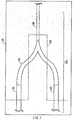
- Fig. 1 shows a configuration of an optical coupler according to an embodiment of the present invention.
- Fig. 2A shows a light wave emitted from the optical coupler according to a conventional manner.
- Fig. 2B shows a light wave emitted from the optical coupler according to an embodiment of the present invention.
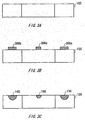
- Fig. 3A shows a manufacturing method of the optical coupler according to an embodiment of the present invention in a substrate preparation step.
- Fig. 3B shows the manufacturing method of the optical coupler according to the embodiment of the present invention in a metal film formation step.
- Fig. 3C shows the manufacturing method of the optical coupler according to the embodiment of the present invention in a diffusion step.
- Fig. 4A shows a manufacturing method of the optical coupler according to a first alternative of the embodiment of the present invention in a substrate preparation step.
- Fig. 4B shows the manufacturing method of the optical coupler according to the first alternative of the embodiment of the present invention in a metal film formation step.
- Fig. 4C shows the manufacturing method of the optical coupler according to the first alternative of the embodiment of the present invention in a diffusion step.
- Fig. 5A shows a manufacturing method of the optical coupler according to a second alternative of the embodiment of the present invention in a substrate preparation step.
- Fig. 5B shows the manufacturing method of the optical coupler according to the second alternative of the embodiment of the present invention in a mask pattern formation step.
- Fig. 5C shows the manufacturing method of the optical coupler according to the second alternative of the embodiment of the present invention in a proton exchange step.
- Fig. 5D shows the manufacturing method of the optical coupler according to the second alternative of the embodiment of the present invention in a mask pattern removal step.
- Fig. 6 shows a configuration of a Mach-Zehnder interferometer according to an embodiment of the present invention.
- Fig. 1 shows a configuration of an optical coupler 120 according to an embodiment.
- the optical coupler 120 is a Y-branching optical coupler which mixes and outputs the first light and the second light from the outside.
- the optical coupler 120 includes a first input optical wave guide 130, a second input optical wave guide 140, an optical coupler 150, and an output optical wave guide 160.
- the first input optical wave guide 130 propagates the first light from the outside, and inputs it into the optical coupler 150.
- the second input optical wave guide 140 propagates the second light from the outside, and inputs it into the optical coupler 150.
- the optical coupler 120 is used as an optical coupler of a Mach-Zehnder light modulator
- the first light and the second light which are branched from the light in the wave guide located upstream of the branching point, may be input into the first input optical wave guide 130 and the second input optical wave guide 140, respectively.
- the optical coupler 150 outputs a mixed light, which is the mixture of the first light from the first input optical wave guide 130 and the second light from the second input optical wave guide 140.
- the output optical wave guide 160 propagates the mixed light, and outputs it from an end.
- the output optical wave guide 160 includes a feature that the percentage per unit length of emitting the light being propagated in the wave guide is higher than that of the first input optical wave guide 130 or the second input optical wave guide 140 so as to improve the extinction ratio of the optical coupler 120. More particularly, a cross section area of the output optical wave guide 160 may be less than a cross section area of the first input optical wave guide 130 or the second input optical wave guide 140, for example.
- a width of the output optical wave guide 160 may be less than that of the first input optical wave guide 130 or the second input optical wave guide 140.
- the percentage of the light emission from the first input optical wave guide 130 and the second input optical wave guide 140 may be reduced by ridge processing of the first input optical wave guide 130 and the second input optical wave guide 140.
- the output optical wave guide 160 may have a higher percentage per unit length of emitting the light being propagated in the optical wave guide to the periphery of the optical wave guide than that of the optical wave guide before being branched.
- the optical coupler 120 is formed on the substrate 100 made of ferroelectric crystals, such as lithium niobate or lithium tantalate.
- the first input optical wave guide 130, the second input optical wave guide 140, the optical coupler 150, and/or the output optical wave guide 160 are made of diffusing metal, such as titanium, into a portion where the optical wave guide is to be formed in a layer of the ferroelectric crystal of the substrate 100.
- the output optical wave guide 160 is formed so that the diffusion of metal, such as titanium, in per unit length, may become less than that of the first input optical wave guide 130 and the second input optical wave guide 140, the output optical wave guide 160 is formed so that the width or the thickness, or the cross section area which is vertical to the wave guide direction may become small.
- the first input optical wave guide 130, the second input optical wave guide 140, the optical coupler 150, and/or the output optical wave guide 160 may be formed by proton exchange of the portion where the optical wave guide is to be formed in the layer of the ferroelectric crystal of the substrate 100.
- the output optical wave guide 160 is formed so that the quantity of proton exchange in per unit length may become less than that of the first input optical wave guide 130 or the second input optical wave guide 140, the output optical wave guide 160 is formed so that the width or the thickness, or the cross section area which is vertical to the wave guide direction may become small.
- Fig. 2A shows a light wave 270 emitted from the optical coupler 120 according to a conventional manner
- Fig. 2B shows a light wave 270 emitted from the optical coupler 120 according to an embodiment of the present invention.
- it is common to form it so that the percentage per unit length of emitting the light being propagated in the optical wave guide to the periphery of the optical wave guide for the first input optical wave guide 130, the second input optical wave guide 140 and the output optical wave guide 260 becomes low so as to reduce the propagation loss of light in the conventional configuration. That is, as for the first input optical wave guide 130, the second input optical wave guide 140, and the output optical wave guide 260, substantially the same optical wave guide is used, of which the refractive index distribution may be determined to sufficiently confine the light to achieve low loss.
- the optical coupler 150 mixes the lights, it becomes the light having higher order mode, and is emitted to the exterior of the output optical wave guide 260 as the light wave 270. Consequently, the light wave does not mixed to the output optical wave guide 260.
- the optical coupler 120 using the first input optical wave guide 130, the second input-side optical wave guide 140, and the output optical wave guide 260 which sufficiently confine the light is used for the first light and the second light having wide wavelength domain, not all emitting light can be emitted to the exterior of the output optical wave guide 260 at the wavelength domain.
- an optical wave guide of the output optical wave guide 160 is formed so that the less light is to be confined in it than the first input optical wave guide 130 and the second input optical wave guide 140. That is, for example, even if it has the same refractive index distribution, the output optical wave guide 160 uses an optical wave guide having small cross section area, width, etc. The percentage per unit length of emitting the light being propagated in the optical wave guide is higher than that of the first input optical wave guide 130 or the second input optical wave guide 140.
- the output optical wave guide 160 leaks out a light energy by the light wave having wide wavelength domain, and facilitates the emission of the higher order mode light being propagated in the output optical wave guide 160. Therefore, the light, which is the mixture of the first light and the second light and became a higher order mode light, is efficiently emitted as the light wave 270, and can reduce the proportion output as the output light from an end of the output optical wave guide 160.
- the optical coupler 120 of the present embodiment a good extinction ratio is realizable by efficiently emitting the higher order mode light caused by the optical coupler 150. Moreover, the above-mentioned structure has a feature that it is smaller and can be manufactured easier than the optical coupler disclosed in Japanese Patent Laid-Open No. 8-194195 and Japanese Patent Laid-Open No. 9-318367.
- Figs. 3A-3C show a manufacturing method of the optical coupler 120 according to the present embodiment.
- Figs. 3A-3C are sectional views taken on line 190 in Fig. 1 and show the structure of the optical coupler 120 in each manufacturing step seen from a side of.the output optical wave guide 160.
- a substrate preparation step the substrate 100 made of a ferroelectric crystal is prepared.
- a titanium film 300a which is an example of a metal film, is formed on the portion where the optical wave guide is to be formed on a surface of the layer of the ferroelectric crystal of the substrate 100.
- a titanium film 300b which is an example of a metal film, is formed on a surface of the layer of the ferroelectric crystal of the substrate 100.
- a titanium film 300c which is an example of a metal film, is formed on the portion where the optical wave guide is to be formed on a surface of the layer of the ferroelectric crystal of the substrate 100.
- portion of the metal in the optical wave guide per unit length is lessened by forming titanium film 300c with a width smaller than that of the first input optical wave guide formation step or the second input optical wave guide formation step.
- the thickness of the titanium film 300c may be the same as the thickness of the titanium film 300a or 300b.
- titanium films 300a-300c are formed with a procedure described below.
- a metal film laminating step a metal film is laminated on the whole surface of the substrate 100.
- mask pattern is formed on portions at which the first input optical wave guide 130, the second input optical wave guide 140, and the output optical wave guide 160 are to be formed, on the metal film laminated on the substrate 100.
- the width of the mask pattern corresponding to the portion where the output optical wave guide 160 is to be formed can be made less than the width of the mask pattern corresponding to the portion where the first input optical wave guide 130 or the second input optical wave guide 140 are to be formed.
- the titanium films 300a-300c are formed on the portion where the optical wave guides are to be formed by removing the portion not being masked by the mask pattern on the metal film laminated on the substrate 100.
- the titanium film 300a is diffused in the substrate 100, and the first input optical wave guide 130 embedded in the layer of the ferroelectric crystal in the substrate 100 is formed.
- the titanium film 300b is diffused in the substrate 100, and the second input optical wave guide 140 embedded in the layer of the ferroelectric crystal in the substrate 100 is formed.
- the titanium film 300c is diffused in the substrate 100, and the output optical wave guide 160 embedded in the layer of the ferroelectric crystal in the substrate 100 is formed.
- the optical coupler 150 is formed, for example like the above-mentioned metal film formation step and the diffusion step.
- the first input optical wave guide 130, the second input optical wave guide 140, and the output optical wave guide 160 having smaller width than the first input optical wave guide 130 or the second input optical wave guide 140 can be formed in the substrate 100, and the optical coupler 120 having a good extinction ratio can be manufactured.
- Figs. 4A-4C show a manufacturing method of the optical coupler 120 according to a first alternative of the present embodiment.
- Figs. 4A-4C are sectional views taken on line 190 in Fig. 1 and show the structure of the optical coupler 120 in each manufacturing step seen from a side of the output optical wave guide 160.
- the substrate 100 made of the ferroelectric crystal is prepared like the example explained with reference to Fig. 3A.
- the titanium films 300a-300c are formed on the surface of the layer of the ferroelectric crystal in the substrate 100.
- portion of the metal for the optical wave guide per unit length is lessened by forming the titanium film 300c thinner than in the first input optical wave guide formation step and in the second input optical wave guide formation step.
- the width of the titanium film 300c may be the same as the width of the titanium film 300a or 300b.
- the titanium films 300a-300c are diffused in the substrate 100, and the first input optical wave guide 130, the second input optical wave guide 140, and the output optical wave guide 160, which are embedded in the layer of the ferroelectric crystal in the substrate 100, are formed, respectively.
- the optical coupler 150 is formed, for example, like the above-mentioned metal film formation step and the diffusion step.
- the first input optical wave guide 130, the second input optical wave guide 140, and the output optical wave guide 160 having smaller width or smaller cross section area than the first input optical wave guide 130 or the second input optical wave guide 140 can be formed in the substrate 100, and the optical coupler 120 having a good extinction ratio can be manufactured.
- Figs. 5A-5D show a manufacturing method of the optical coupler 120 according to a second alternative of the present embodiment.
- Figs. 5A-5D are sectional views taken on line 190 in Fig. 1 and show the structure of the optical coupler 120 in each manufacturing step seen from a side of the output optical wave guide 160.
- a substrate preparation step the substrate 100 made of a ferroelectric crystal is prepared like the example explained with reference to Fig. 3A.
- a mask pattern formation step in each of a first input optical wave guide formation step, a second input optical wave guide formation step, and an output optical wave guide formation step a mask pattern 500, which has openings 510a-510c at the portions where the first input optical wave guide 130, the second input optical wave guide 140, and the output optical wave guide 160 are to be formed, is formed.
- the width of opening 510c at the portion where the output optical wave guide 160 is to be formed is less than the width of the opening 510a or 510b at the portion where the first input optical wave guide 130 or the second input optical wave guide 140 is to be formed.
- a portion exposed from the surface mask pattern 500 of the substrate 100 is immersed in liquid including benzoic acid, proton exchange is carried out, and then the first input optical wave guide 130, the second input optical wave guide 140, and the output optical wave guide 160 are formed.
- the width of the opening 510c is less than the width of the opening 510a or 510b, amount of proton exchange per unit length in the opening 510c at the portion where the output optical wave guide 160 is to be formed can be made less than amount of proton exchange per unit length in the opening 510a or 510b at the portion where the first input optical wave guide 130 or the second input optical wave guide 140 is to be formed.
- the mask pattern 500 is removed in a mask pattern removal step.
- the first input optical wave guide 130, the second input optical wave guide 140, and the output optical wave guide 160 having smaller width or smaller cross section area than the first input optical wave guide 130 or the second input optical wave guide 140 can be formed by the proton exchange on the substrate 100, and the optical coupler 120 having a good extinction ratio can be manufactured.
- width of the opening 510c is made less than the width of the opening 510a or 510b, it is possible to make the widths of the openings 510a-510c substantially the same as one another, and make duration of the proton exchange for the opening 510c at the portion where the output optical wave guide 160 is to be formed to be shorter than duration of the proton exchange for the opening 510a or 510b at the portion where the first input optical wave guide 130 or the second input optical wave guide 140 is to be formed.
- Fig. 6 shows a configuration of a Mach-Zehnder interferometer 600 according to the present embodiment.
- the Mach-Zehnder interferometer 600 includes an optical branch 610 which branches the input light, and the optical mixer 615 which mixes two lights which have been branched by the optical branch 610.
- the optical coupler 120 shown in Fig. 1 is used as the optical mixer 615 of the Mach-Zehnder interferometer 600 according to the present embodiment.
- the optical coupler 120 shown in Fig. 1 may be further used as the optical branch 610 of the Mach-Zehnder interferometer 600.
- the optical branch 610 includes a before-branch optical wave guide 620, an optical branch 630, and the first input optical wave guide 130 and the second input optical wave guide 140 for a side of the optical branch 630.
- the first input optical wave guide 130, the second input optical wave guide 140, the optical branch 630, and the before-branch optical wave guide 620 of the optical branch 610 correspond to the first input optical wave guide 130, the second input optical wave guide 140, the optical coupler 150, and the output optical wave guide 160 of the optical coupler 120 shown in Fig. 1, respectively.
- the before-branch optical wave guide 620 propagates the light from the outside to the optical branch 630.
- the optical branch 630 branches the light from the before-branch optical wave guide 620, and the first light is input into the first input optical wave guide 130, and the second light is input into the second input optical wave guide 140, respectively.
- the first input optical wave guide 130 and the second input optical wave guide 140 propagate the first light and the second light which were input from the optical branch 630.
- the optical mixer 615 includes the first input optical wave guide 130 and the second input optical wave guide 140 for a side of the optical coupler 150, the optical coupler 150, and the output optical wave guide 160. Since these components are equivalent to the components bearing the same reference numeral shown in Fig. 1, respectively, the explanation will be omitted.
- the Mach-Zehnder interferometer 600 may be used as a bi-directional Mach-Zehnder interferometer 600 operable to output the branched and mixed light input into the before-branch optical wave guide 620 from the output optical wave guide 160, while outputting the branched and mixed light input into the output optical wave guide 160 from the before-branch optical wave guide 620.
- the Mach-Zehnder interferometer 600 having a good extinction ratio can be provided.
Landscapes
- Physics & Mathematics (AREA)
- Engineering & Computer Science (AREA)
- Microelectronics & Electronic Packaging (AREA)
- General Physics & Mathematics (AREA)
- Optics & Photonics (AREA)
- Optical Integrated Circuits (AREA)
- Optical Modulation, Optical Deflection, Nonlinear Optics, Optical Demodulation, Optical Logic Elements (AREA)
Applications Claiming Priority (2)
| Application Number | Priority Date | Filing Date | Title |
|---|---|---|---|
| JP2003423537 | 2003-12-19 | ||
| JP2003423537A JP2005181757A (ja) | 2003-12-19 | 2003-12-19 | マッハ・ツェンダー干渉計、光結合器及び光結合器の製造方法 |
Publications (1)
| Publication Number | Publication Date |
|---|---|
| EP1544646A1 true EP1544646A1 (de) | 2005-06-22 |
Family
ID=34510713
Family Applications (1)
| Application Number | Title | Priority Date | Filing Date |
|---|---|---|---|
| EP04078456A Withdrawn EP1544646A1 (de) | 2003-12-19 | 2004-12-17 | Mach-Zehnder Interferometer, optischer Koppler und Verfahren zu seiner Herstellung |
Country Status (3)
| Country | Link |
|---|---|
| US (1) | US20050135750A1 (de) |
| EP (1) | EP1544646A1 (de) |
| JP (1) | JP2005181757A (de) |
Cited By (1)
| Publication number | Priority date | Publication date | Assignee | Title |
|---|---|---|---|---|
| CN108871307A (zh) * | 2018-04-25 | 2018-11-23 | 北京航空航天大学 | 基于图像识别与光功率反馈的y波导芯片自动直接耦合装置 |
Families Citing this family (2)
| Publication number | Priority date | Publication date | Assignee | Title |
|---|---|---|---|---|
| WO2012099606A1 (en) | 2011-01-21 | 2012-07-26 | Hewlett-Packard Development Company, L.P. | Wavefront synthesizer systems |
| RU2754205C1 (ru) * | 2020-12-17 | 2021-08-30 | Федеральное государственное бюджетное учреждение науки Физико-технический институт им. А.Ф. Иоффе Российской академии наук | Способ подстройки интегрально-оптического интерферометра маха-цендера |
Citations (3)
| Publication number | Priority date | Publication date | Assignee | Title |
|---|---|---|---|---|
| US5193136A (en) * | 1989-10-27 | 1993-03-09 | Litton Systems, Inc. | Process for making multifunction integrated optics chips having high electro-optic coefficients |
| WO2001029595A1 (en) * | 1999-10-15 | 2001-04-26 | California Institute Of Technology | Titanium-indiffusion waveguides |
| US20030031401A1 (en) * | 2001-08-08 | 2003-02-13 | Codeon Corporation | Apparatus and method to increase the extinction ratio in a Mach-Zehnder interferometer |
-
2003
- 2003-12-19 JP JP2003423537A patent/JP2005181757A/ja not_active Withdrawn
-
2004
- 2004-12-17 EP EP04078456A patent/EP1544646A1/de not_active Withdrawn
- 2004-12-17 US US11/015,064 patent/US20050135750A1/en not_active Abandoned
Patent Citations (3)
| Publication number | Priority date | Publication date | Assignee | Title |
|---|---|---|---|---|
| US5193136A (en) * | 1989-10-27 | 1993-03-09 | Litton Systems, Inc. | Process for making multifunction integrated optics chips having high electro-optic coefficients |
| WO2001029595A1 (en) * | 1999-10-15 | 2001-04-26 | California Institute Of Technology | Titanium-indiffusion waveguides |
| US20030031401A1 (en) * | 2001-08-08 | 2003-02-13 | Codeon Corporation | Apparatus and method to increase the extinction ratio in a Mach-Zehnder interferometer |
Cited By (2)
| Publication number | Priority date | Publication date | Assignee | Title |
|---|---|---|---|---|
| CN108871307A (zh) * | 2018-04-25 | 2018-11-23 | 北京航空航天大学 | 基于图像识别与光功率反馈的y波导芯片自动直接耦合装置 |
| CN108871307B (zh) * | 2018-04-25 | 2021-11-26 | 北京航空航天大学 | 基于图像识别与光功率反馈的y波导芯片直接耦合装置 |
Also Published As
| Publication number | Publication date |
|---|---|
| US20050135750A1 (en) | 2005-06-23 |
| JP2005181757A (ja) | 2005-07-07 |
Similar Documents
| Publication | Publication Date | Title |
|---|---|---|
| US20090190876A1 (en) | Waveguide polarizer and optical waveguide device | |
| CA1168487A (en) | Hybrid optical junction and its use in a loop interferometer | |
| US20150261064A1 (en) | Multi-port optical circulator system | |
| WO2010082673A1 (ja) | 分岐型光導波路、光導波路基板および光変調器 | |
| US4953935A (en) | Integrated optic star coupler | |
| US5875276A (en) | Guided wave device and method of fabrication thereof | |
| Samanta et al. | A 1× 2 polarization-independent power splitter using three-coupled silicon rib waveguides | |
| JPH07318986A (ja) | 導波路型光スイッチ | |
| Nakajima et al. | Crosstalk characteristics of Ti-LiNbO 3 intersecting waveguides and their application as TE/TM mode splitters | |
| US20050135750A1 (en) | Mach-zehnder interferometer, optical coupler, and manufacturing method of optical coupler | |
| JP2007114222A (ja) | 光制御素子 | |
| Maruyama et al. | TE-TM mode splitter using directional coupling between heterogeneous waveguides in LiNbO/sub 3 | |
| JPH02234108A (ja) | 光分岐・合波回路 | |
| JPS62183405A (ja) | テ−パ付光導波回路及びその製造方法 | |
| CN114467044A (zh) | 光波导路元件 | |
| JP3220003B2 (ja) | 偏光分離素子 | |
| CN108693599B (zh) | 光波导元件 | |
| Chen et al. | Integrated optical beam splitters formed in glass channel waveguides having variable weighting as determined by mask dimensions | |
| JP2004145246A (ja) | 平面型二次元導波路および二次元導波路型光学装置 | |
| JP2002162658A (ja) | 光導波路素子及び光波長変換装置 | |
| JP2687923B2 (ja) | 光非相反回路とその製造方法 | |
| JPH07191225A (ja) | 導波路型光アイソレータ | |
| JPS61122610A (ja) | 光フアイバ端面加工方法 | |
| Mueller et al. | Integrated Optics Comporents For Fiber Gyroscopes and Observation of the Photorefractive Effect in LiNbO [sub] 3 [/sub] Directional Couplers at GaAs Wavelengths | |
| US5834055A (en) | Guided wave device and method of fabrication thereof |
Legal Events
| Date | Code | Title | Description |
|---|---|---|---|
| PUAI | Public reference made under article 153(3) epc to a published international application that has entered the european phase |
Free format text: ORIGINAL CODE: 0009012 |
|
| AK | Designated contracting states |
Kind code of ref document: A1 Designated state(s): AT BE BG CH CY CZ DE DK EE ES FI FR GB GR HU IE IS IT LI LT LU MC NL PL PT RO SE SI SK TR |
|
| AX | Request for extension of the european patent |
Extension state: AL BA HR LV MK YU |
|
| 17P | Request for examination filed |
Effective date: 20050718 |
|
| AKX | Designation fees paid |
Designated state(s): DE GB |
|
| STAA | Information on the status of an ep patent application or granted ep patent |
Free format text: STATUS: THE APPLICATION IS DEEMED TO BE WITHDRAWN |
|
| 18D | Application deemed to be withdrawn |
Effective date: 20060707 |