EP1544130B1 - Verpackugsbehältnis mit Leistungshalbleitermodul - Google Patents
Verpackugsbehältnis mit Leistungshalbleitermodul Download PDFInfo
- Publication number
- EP1544130B1 EP1544130B1 EP04025144A EP04025144A EP1544130B1 EP 1544130 B1 EP1544130 B1 EP 1544130B1 EP 04025144 A EP04025144 A EP 04025144A EP 04025144 A EP04025144 A EP 04025144A EP 1544130 B1 EP1544130 B1 EP 1544130B1
- Authority
- EP
- European Patent Office
- Prior art keywords
- power semiconductor
- semiconductor module
- packaging container
- cover surface
- shaped
- Prior art date
- Legal status (The legal status is an assumption and is not a legal conclusion. Google has not performed a legal analysis and makes no representation as to the accuracy of the status listed.)
- Expired - Lifetime
Links
Images


Classifications
-
- B—PERFORMING OPERATIONS; TRANSPORTING
- B65—CONVEYING; PACKING; STORING; HANDLING THIN OR FILAMENTARY MATERIAL
- B65D—CONTAINERS FOR STORAGE OR TRANSPORT OF ARTICLES OR MATERIALS, e.g. BAGS, BARRELS, BOTTLES, BOXES, CANS, CARTONS, CRATES, DRUMS, JARS, TANKS, HOPPERS, FORWARDING CONTAINERS; ACCESSORIES, CLOSURES, OR FITTINGS THEREFOR; PACKAGING ELEMENTS; PACKAGES
- B65D25/00—Details of other kinds or types of rigid or semi-rigid containers
- B65D25/02—Internal fittings
- B65D25/10—Devices to locate articles in containers
- B65D25/106—Elements projecting into a recess or through a hole in the articles
-
- B—PERFORMING OPERATIONS; TRANSPORTING
- B65—CONVEYING; PACKING; STORING; HANDLING THIN OR FILAMENTARY MATERIAL
- B65D—CONTAINERS FOR STORAGE OR TRANSPORT OF ARTICLES OR MATERIALS, e.g. BAGS, BARRELS, BOTTLES, BOXES, CANS, CARTONS, CRATES, DRUMS, JARS, TANKS, HOPPERS, FORWARDING CONTAINERS; ACCESSORIES, CLOSURES, OR FITTINGS THEREFOR; PACKAGING ELEMENTS; PACKAGES
- B65D81/00—Containers, packaging elements, or packages, for contents presenting particular transport or storage problems, or adapted to be used for non-packaging purposes after removal of contents
- B65D81/02—Containers, packaging elements, or packages, for contents presenting particular transport or storage problems, or adapted to be used for non-packaging purposes after removal of contents specially adapted to protect contents from mechanical damage
- B65D81/025—Containers made of sheet-like material and having a shape to accommodate contents
Definitions
- the invention describes a packaging container with power semiconductor modules for their internal and / or external transport.
- Modern power semiconductor modules especially with power transistors such as IGBT (insulated gate bipolar transistor) or MOS-FET (metal oxide semiconductor field effect transistor) are very sensitive to touch by the human hand, because this can discharge electrostatic fields on the contact elements and damage the power transistors or destroy.
- any type of contamination by way of example of the contact elements or, especially in the case of baseplate-free power semiconductor modules, also of the underside of the substrate is disadvantageous. In this case, the electrical contact safety is impaired in later operation.
- Substrate surfaces especially if they are already provided with a pasty thermally conductive layer before transport, also require protection against contact and / or contamination.
- the starting point of the invention is the own patent DE 39 09 898 C2 and the non-prepublished own patent application DE 103 06 643 A1 and DE 103 20 186 A1 ,
- the DE 39 09 898 C2 discloses a packaging container for power semiconductor modules according to the prior art. These were often power semiconductor modules constructed of thyristors. Such power semiconductor modules are exemplary insensitive to electrostatic charging. Therefore, this document proposes a stackable packaging, which preferably consists of a cardboard box. However, such packaging can also protect against electrostatic discharge with a suitable choice of cardboard packaging therein the power semiconductor module. One Protection against contact of the connection elements with the packaging itself, on the other hand, can not be achieved.
- the DE 103 06 643 A1 presents a modern power semiconductor module having on a surface a plurality of connection elements. Since such power semiconductor modules according to the prior art are usually equipped with power transistors and power diodes, at least some of the connection elements are sensitive to electrostatic discharge.
- the surface of the power semiconductor module opposite the connection elements here has an outer metallic layer as part of the substrate. Even such surfaces require protection against contamination, especially by contact with the human hand. Any type of contamination adversely affects the adhesiveness of a thermally conductive layer, ie its function as an intermediate layer between the power semiconductor module and a heat sink necessary for its operation. As a result, the heat generated in the power semiconductor module can not be dissipated in the intended manner, whereby operation at full capacity of the power semiconductor module is not possible.
- the DE 103 20 186 A1 discloses a thermal paste for a power semiconductor module, which is already provided by the manufacturer with a thermally conductive pasty layer. This is advantageous because in this way the suitable thermally conductive layer can be applied with a layer thickness matched to the power semiconductor module. It is also advantageous that this simplifies the assembly after transport since no layers of the order of 100 .mu.m need to be applied homogeneously here.
- the document provides for the protection of these layers, a protective cover, which is placed on the power semiconductor module and having nubs such that the heat-conductive layer is touched only a small part of this protective cover. Thus, it is ensured that after removal of this protective cover, the thermally conductive layer is almost intact and remains fully functional.
- thermal grease power semiconductor module can be transported with a protective case, for example in the above-mentioned packaging container.
- a protective case for example in the above-mentioned packaging container.
- the protective cover is advantageously placed only once and removed after transport. Repeated use, as is necessary for example during in-house transport, can not afford this protective cover suitable.
- the CA 2 372 480 A1 discloses a packaging container for shock-sensitive products, preferably computer components such as hard disks, CD or DVD drives and CPUs.
- the packaging container consists of at least one molded body with a wall, which has either on two opposite wall sections each have a supporting edge or at least three locations of the wall depending on a support surface which serve the shock absorption of the product contained.
- the top surface of the packaging container has a depression in the interior thereof, which preferably has a planar contact surface to the shock-sensitive product and this supports.
- the JP 09 290891 A discloses a transport carrier container for electronic components with a housing and at least one cable connection.
- the top surface of a U-shaped molded body is designed to its inner volume as a pedestal with surrounding, protruding slats and serves the purpose to let the component rest at its junction between the housing and cable connection.
- the object of the present invention is to provide a packaging container with at least one power semiconductor module for its internal and / or external transport which protects surfaces sensitive to contamination and / or other parts of the power semiconductor module and / or contact elements of the power semiconductor module which are sensitive to electrostatic fields and a multiple Use of this packaging container allowed.
- the basic idea of the packaging container according to the invention with at least one power semiconductor module is based on at least one molded body.
- This shaped body has a wall and a preferably completely closed cover surface.
- the wall is divided into several wall sections. At least two opposite wall sections each have a support edge or arranged at least three locations of the wall depending on a support surface. This support edges or support surfaces form a support for certain parts of the power semiconductor module such that contact of the power semiconductor module is prevented with the top surface of the molding.
- the power semiconductor module is at least partially at wall sections, or at least closely adjacent thereto arranged what is used synonymously here.
- the packaging container has at least one support on the top surface of the shaped body. This support extends from the top surface into the interior of the molded body, wherein it tapers from the top surface into the interior and partially extends into a recess of the power semiconductor module and thereby prevents contact of the power semiconductor module with the top surface.
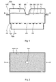
- Fig. 1 shows a first embodiment of a packaging container with a power semiconductor module consisting of two individual moldings.
- Fig. 2 shows a packaging container Fig. 1 in an orthogonal plane.
- Fig. 3 shows a second embodiment of a packaging container with a power semiconductor module consisting of two interconnected moldings.
- Fig. 4 shows a packaging container Fig. 3 in an orthogonal plane.
- Fig. 5 shows a third embodiment of a packaging container with a power semiconductor module consisting of two interconnected moldings.
- Fig. 6 shows a packaging container Fig. 5 in an orthogonal plane.
- Fig. 1 shows a first embodiment of a packaging container with a power semiconductor module (200) consisting of two individual moldings (100). Shown is a cross section through the packaging container and a power semiconductor module (200) embedded therein along the section line AA of FIG Fig. 2 ,
- the first mold body (100a) forms the bottom part, the second mold body (100b) the lid part.
- Both moldings (100) are preferably made of the same material, here a thermoformed plastic film with a thickness of 500 .mu.m.
- This plastic film consists of a dissipative plastic according to DIN IEC 61340 to protect the power semiconductor module (200) against electrostatic discharges.
- the wall of the bottom part (100a) consists of four rectangularly arranged wall sections (110a). Here, two mutually opposite wall sections (110a) each have a supporting edge (112). Furthermore, the bottom part (100a) has a closed cover surface, the bottom (120a). The opposite side is designed to be open to insert a power semiconductor module (200) in this bottom part (110a) can.
- This power semiconductor module (200) consists of a plastic housing (202) and has metallic connection elements (222) on the side (220) facing the bottom (120a). These connection elements (222) should not come into contact with the Verpackurigs internis for their protection. Therefore, the power semiconductor module (200) rests with a part of its housing (202) on the supporting edges (112a).
- the housing (202) of the power semiconductor module (200) partly rests on the wall sections (110a) or has only a slight distance therefrom, what is considered synonymous here.
- the support edges (112) must therefore be formed in their surface extent such that slipping of the power semiconductor module (200) from the supporting edges (112) is not possible by a slight horizontal change in position due to the distance of the power semiconductor module (200) to the wall sections (110a) is.
- contact of the connection elements (222) of the power semiconductor module (200) with the packaging container is effectively prevented.
- a packaging container as described so far is sufficient in most cases for in-house transport.
- the packaging container preferably also has a second molded part (100b), the lid part, on.
- This cover part also consists of four rectangularly arranged wall sections (110b).
- the cover part (100b) has a closed cover surface, the cover (120b).
- the power semiconductor module (200) described here has a centrally located recess (214), a mounting hole (cf. Fig. 2 ) on; the lid (110b) of the lid part (100b) therefore has a support (122).
- This preferably cone or truncated pyramid shaped support (122) extends from the cover (120b) towards the interior of the cover part (100b). Due to its conical or truncated pyramidal shape, it tapers in the direction of the power semiconductor module (200).
- the support (122) extends into the recess (214) of the power semiconductor module (200). This results in only a very small contact surface with the power semiconductor module (200).
- the illustrated power semiconductor module (200) has on its side facing the cover (110b), ie on the substrate (210), a thermally conductive pasty layer, a thermal paste (212) according to the prior art. This must be protected against contact and contamination. This is also achieved with the cover part (100b) presented here.
- the cover part (100b) rests against the power semiconductor module (200) only with the small area of the support (122) formed in it, and thus only against the thermal compound (212) there.
- the cover part (100b) in conjunction with the bottom part (100a) sufficiently protects the connection elements (222) and the thermal compound (212) and thus the entire power semiconductor module (200) for internal and external transport.
- Fig. 2 shows a packaging container Fig. 1 however, in a section in an orthogonal plane along the section line BB of the Fig. 1 , Shown are the wall sections (110b) of the rectangular wall of the cover part (100b) and the power semiconductor module (200) with its thermal compound (212) arranged on the substrate. Furthermore, the central recess (214) of the power semiconductor module is shown, in which the support (122) (see. Fig. 1 ) extends into it.
- Fig. 3 shows a second embodiment of a packaging container with a power semiconductor module (200) consisting of two interconnected moldings (100). Shown is a cross-section through the packaging container and a power semiconductor module (200) embedded therein along the section line AA of FIG Fig. 4 ,
- the bottom part (100a) also has a rectangular wall with four wall sections (110a).
- the floor (120a) has four frusto-conical supports (122). These supports (122) protrude into four mounting holes (214) of the power semiconductor module (200).
- the latter On the side of the power semiconductor module (200) facing the bottom (110a), the latter in turn has a substrate (210) with an outer metallic layer which is covered with a thermal compound (212).
- the four supports (122) now space the power semiconductor module (200) or its substrate (210) with the thermal paste (212) from the bottom (120a) so that the thermal paste (212) and the bottom (110a) only at the contact surfaces between the supports (122) and the power semiconductor module (200). This ensures that, during transport, the thermal compound (212) is modified neither in its layer thickness nor in its homogeneity. Protection against contamination is also given.
- the protection against contamination of the entire power semiconductor module (200) is ensured by the packaging container having a lid part (100b) which is integrally connected to the bottom part (100a) via another mold part (300).
- An advantage of this embodiment of the packaging container is that it can be closed gas-tight by a peripheral seal and thus represents an ideal protection for the external transport of a power semiconductor module (200).
- the cover part (100b) is configured with a rectangular wall, wherein here all four wall sections (110b) have support edges (112) and the power semiconductor module (200) in the area between the support edges (112) and the opening of the cover part (100b) at the wall sections (110b) is present.
- the support edges (112) ensure that the cover (110b) has no contact points with the connection elements (222) of the power semiconductor module (200).
- Fig. 4 shows a packaging container Fig. 3 however, in a section in an orthogonal plane along the section line BB of the Fig. 3 , Shown are the wall sections (110a) of the rectangular wall of the bottom part (100a), and the power semiconductor module (200) with its on the substrate (210) arranged thermal compound (212). Furthermore, the four mounting holes (214) of the power semiconductor module (200) are shown, in which the four supports (122) (see. Fig. 3 ) extend into it.
- Fig. 5 shows a third embodiment of a packaging container with a power semiconductor module (200) consisting of two interconnected moldings (100). Shown is a cross section through the packaging container and a power semiconductor module (200) embedded therein along the section line AA of FIG Fig. 6 ,
- the power semiconductor module (200) shown here consists of a housing (202) and a base plate (230), according to the prior art, a copper plate with a thickness of 10 mm.
- the bottom part (100a) in turn has a rectangular wall, in which case in the corners between two wall sections (110a) supporting surfaces (114) (see. Fig. 6 ) are arranged.
- the power semiconductor module (200) bears with its corners on these support surfaces (114) and rests with a part of its base plate (230) on the wall sections (110a) of the base part (100a). This horizontal slipping during transport only to the extent possible, as the power semiconductor module (200) always rests on all support surfaces (114) and thus a contact between the bottom (110a) and the connection elements (222) of the power semiconductor module (200) is effectively prevented ,
- the lid part (100b) of the packaging container is again as in Fig. 3 integrally connected to the bottom part (100a). In turn, it has supports (122) which protrude into the four fastening bores (214) of the power semiconductor module (200).
- a packaging container (not shown) for a power semiconductor module (200) designed as a disk cell has at least three spacer surfaces (114) preferably arranged in an equilateral triangle on a circular wall (110a), on which the housing of the disk cell rests.
- Fig. 6 shows a packaging container Fig. 5 however, in a section in an orthogonal plane along the section line BB of the Fig. 5 , Shown are the wall portions (110a) of the rectangular wall of the bottom part (100a) and the power semiconductor module (200) with its on the base plate (230) arranged thermal compound (212). Hatched here are one of the four identical support surfaces (114) arranged in the corners of the respective wall sections (110a). On these support surfaces (114), the base plate (230) of the power semiconductor module (200) is located. Furthermore, the four mounting holes (214) of the power semiconductor module (200) are shown, in which the four supports (122) (see. Fig. 5 ) of the lid part (100b).
Landscapes
- Engineering & Computer Science (AREA)
- Mechanical Engineering (AREA)
- Packaging Frangible Articles (AREA)
- Inverter Devices (AREA)
- Packages (AREA)
- Coupling Device And Connection With Printed Circuit (AREA)
Description
- Die Erfindung beschreibt ein Verpackungsbehältnis mit Leistungshalbleitermodulen zu deren inner- und / oder außerbetrieblichen Transport. Moderne Leistungshalbleitermodule, speziell mit Leistungstransistoren wie IGBT (insulated gate bipolar transistor) oder MOS-FET (metal oxid semiconductor field effect transistor) sind sehr empfindliche gegenüber Berührungen durch die menschliche Hand, weil sich hierdurch elektrostatische Felder auf die Kontaktelemente entladen können und die Leistungstransistoren vorschädigen oder zerstören können. Weiterhin sind jegliche Art von Verschmutzungen beispielhaft der Kontaktelemente oder speziell bei grundplattenlosen Leistungshalbleitermodulen auch der Substratunterseite nachteilig. Hierbei wird die elektrische Kontaktsicherheit im späteren Betrieb beeinträchtigt. Substratunterseiten, speziell wenn sie bereits vor dem Transport mit einer pastösen wärmeleitfähigen Schicht versehen sind, bedürfen ebenfalls eines Schutzes vor Berührung und / oder Verunreinigung.
- Ausgangspunkt der Erfindung sind das eigene Patent
DE 39 09 898 C2 sowie die nicht vorveröffentlichten eigenen PatentanmeldungDE 103 06 643 A1 undDE 103 20 186 A1 . DieDE 39 09 898 C2 offenbart ein Verpackungsbehältnis für Leistungshalbleitermodule nach dem damaligen Stand der Technik. Hierbei handelte es sich häufig um Leistungshalbleitermodule aufgebaut aus Thyristoren. Derartige Leistungshalbleitermodule sind beispielhaft gegen elektrostatische Aufladung unempfindlich. Daher schlägt diese Druckschrift eine stapelbare Verpackung vor, die vorzugsweise aus einer Kartonage besteht. Derartige Verpackungen können allerdings bei geeigneter Wahl der Kartonage das darin befindliche Leistungshalbleitermodul auch gegen elektrostatische Entladungen schützen. Ein Schutz gegen Kontakt der Anschlusselemente mit der Verpackung selbst demgegenüber nicht erzielbar. - Die
DE 103 06 643 A1 stellt ein modernes Leistungshalbleitermodul vor, welches auf einer Oberfläche eine Mehrzahl von Anschlusselementen aufweist. Da derartige Leistungshalbleitermodule nach dem Stand der Technik meist mit Leistungstransistoren und Leistungsdioden bestückt sind, sind zumindest einige der Anschlusselemente empfindlich gegen elektrostatische Entladung. Die den Anschlusselementen gegenüberliegende Oberfläche des Leistungshalbleitermodul weist hier eine außen liegende metallische Schicht als Teil des Substrats auf. Auch derartige Oberflächen bedürfen eines Schutzes gegen Verschmutzung, speziell auch durch Kontakt mit der menschlichen Hand. Durch jegliche Art von Verschmutzung wird die Haftfähigkeit einer wärmeleitfähigen Schicht, also ihre Funktion als Zwischenschicht zwischen dem Leistungshalbleitermodul und einem zu dessen Betrieb notwendigen Kühlkörper, beeinträchtigt. Hierdurch kann die im Leistungshalbleitermodul entstehende Wärme nicht in vorgesehener Weise abgeführt werden, wodurch ein Betrieb bei voller Leistungsfähigkeit des Leistungshalbleitermoduls nicht möglich ist. - Die
DE 103 20 186 A1 offenbart eine Wärmeleitpaste für ein Leistungshalbleitermodul, welches bereits beim Hersteller mit einer wärmeleitfähigen pastösen Schicht versehen wird. Dies ist vorteilhaft, weil hierdurch die geeignete wärmeleitfähige Schicht mit einer auf das Leistungshalbleitermodul abgestimmten Schichtdicke aufgetragen werden kann. Weiterhin vorteilhaft ist, dass hierdurch die Montage nach dem Transport vereinfacht wird, da hier keine Schichten in der Größenordnung von 100µm homogen aufgebracht werden müssen. Die Druckschrift stellt zum Schutz dieser Schichten eine Schutzhülle vor, die auf das Leistungshalbleitermodul aufgesetzt wird und Noppen derart aufweist, dass die wärmeleitfähige Schicht nur zu einem geringen Teil von dieser Schutzhülle berührt wird. Somit ist gewährleistet, dass nach Entfernen dieser Schutzhülle die wärmeleitfähige Schicht annährend unversehrt ist und vollständig funktionsfähig bliebt. Somit können derartige mit einer Wärmeleitpaste versehene Leistungshalbleitermodul mit einer Schutzhülle beispielhaft in oben genanntem Verpackungsbehältnis transportiert werden. Nachteilig ist hierbei allerdings, dass die Schutzhülle vorteilhafterweise nur einmal aufgesetzt und nach dem Transport abgenommen wird. Mehrmaliges Verwenden, wie es beispielhaft beim innerbetrieblichen Transport notwendig ist, kann diese Schutzhülle nicht geeignet leisten. - Die
CA 2 372 480 A1 offenbart ein Verpackungsbehältnis für stoßempfindliche Produkte, vorzugsweise Computerkomponenten wie Festplatten, CD- oder DVD-Laufwerke und CPU's. Das Verpackungsbehältnis besteht aus mindestens einem Formkörper mit einer Wandung, wobei diese entweder an zwei gegenüberliegenden Wandungsabschnitten je eine Abstützkante oder an mindestens drei Stellen der Wandung je eine Abstützfläche aufweist, welche der Stoßdämpfung des enthaltenen Produkts dienen. Zusätzlich weist die Deckfläche des Verpackungsbehältnisses eine Vertiefung in dessen Innenraum auf, welche vorzugsweise eine planare Kontaktfläche zum stoßempfindlichen Produkt aufweist und dieses stützt. - Die
JP 09 290891 A - Die vorliegende Erfindung hat die Aufgabe ein Verpackungsbehältnis mit mindestens einem Leistungshalbleitermodul für deren inner- und / oder außerbetrieblichen Transport zu schaffen, das gegen Verunreinigungen empfindliche Oberflächen und / oder sonstige Teile des Leistungshalbleitermoduls und / oder gegen elektrostatische Felder empfindliche Kontaktelemente des Leistungshalbleitermoduls schützt sowie eine mehrfache Nutzung dieses Verpackungsbehältnisses erlaubt.
- Die Aufgabe wird gelöst durch ein Verpackungsbehältnis mit den Merkmalen des Anspruchs 1. Bevorzugte Weiterbildungen finden sich in den Unteransprüchen.
- Der Grundgedanke des erfindungsgemäßen Verpackungsbehältnisses mit mindestens einem Leistungshalbleitermodul geht aus von mindestens einem Formkörper. Dieser Formkörper weist eine Wandung sowie eine vorzugsweise vollständig geschlossene Deckfläche auf. Die Wandung ist in mehrere Wandungsabschnitte unterteilt. An mindestens zwei gegenüberliegenden Wandungsabschnitten ist je eine Abstützkante oder an mindestens drei Stellen der Wandung je eine Abstützfläche angeordnet. Diese Abstützkanten oder Abstützflächen bilden eine Auflage für bestimmte Teile des Leistungshalbleitermoduls derart, dass eine Berührung des Leistungshalbleitermoduls mit der Deckfläche des Formkörpers verhindert ist. Weiterhin liegt das Leistungshalbleitermodul zumindest teilweise an Wandungsabschnitten an, oder ist zumindest eng benachbart hierzu angeordnet, was hier synonym verwendet wird. Alternativ und zusätzlich weist das Verpackungsbehältnis an der Deckfläche des Formkörpers mindestens eine Stütze auf. Diese Stütze erstreckt sich von der Deckfläche in das Innere des Formkörpers, wobei es sich von der Deckfläche aus ins Innere hinein verjüngt und sich teilweise in eine Aussparung des Leistungshalbleitermoduls hinein erstreckt und hierdurch eine Berührung des Leistungshalbleitermoduls mit der Deckfläche verhindert.
- Nachfolgend werden die Merkmale und Ausgestaltungen der Erfindung anhand der
Fig. 1 bis 6 beispielhaft erläutert. -
Fig. 1 zeigt eine erste Ausgestaltung eines Verpackungsbehältnisses mit einem Leistungshalbleitermodul bestehend aus zwei einzelnen Formkörpern. -
Fig. 2 zeigt ein Verpackungsbehältnis nachFig. 1 in einer hierzu orthogonalen Ebene. -
Fig. 3 zeigt eine zweite Ausgestaltung eines Verpackungsbehältnisses mit einem Leistungshalbleitermodul bestehend aus zwei miteinander verbundenen Formkörpern. -
Fig. 4 zeigt ein Verpackungsbehältnis nachFig. 3 in einer hierzu orthogonalen Ebene. -
Fig. 5 zeigt eine dritte Ausgestaltung eines Verpackungsbehältnisses mit einem Leistungshalbleitermodul bestehend aus zwei miteinander verbundenen Formkörpern. -
Fig. 6 zeigt ein Verpackungsbehältnis nachFig. 5 in einer hierzu orthogonalen Ebene. -
Fig. 1 zeigt eine erste Ausgestaltung eines Verpackungsbehältnisses mit einem Leistungshalbleitermodul (200) bestehend aus zwei einzelnen Formkörpern (100). Gezeigt ist ein Querschnitt durch das Verpackungsbehältnis und eine darin eingebettetes Leistungshalbleitermodul (200) entlang der Schnittlinie A-A derFig. 2 . Der erste Formkörper (100a) bildet hierbei das Bodenteil, der zweite Formkörper (100b) das Deckelteil. Beide Formkörper (100) bestehen vorzugsweise aus dem gleichen Material, hier einer tiefgezogenen Kunststofffolie mit einer Stärke von 500µm. Diese Kunststofffolie besteht aus einem ableitfähigen Kunststoff gemäß DIN IEC 61340 um das Leistungshalbleitermodul (200) gegen elektrostatische Entladungen zu schützen. - Die Wandung des Bodenteils (100a) besteht aus vier rechteckig angeordneten Wandungsabschnitten (110a). Hierbei weisen zwei einander gegenüberliegende Wandungsabschnitte (110a) je eine Abstützkante (112) auf. Weiterhin weist das Bodenteil (100a) eine geschlossene Deckfläche, den Boden (120a), auf. Die gegenüberliegende Seite ist offen gestaltet um ein Leistungshalbleitermodul (200) in dieses Bodenteil (110a) einlegen zu können. Dieses Leistungshalbleitermodul (200) besteht aus einem Kunststoffgehäuse (202) und weist auf der dem Boden (120a) zugewandten Seite (220) metallische Anschlusselemente (222) auf. Diese Anschlusselemente (222) sollen zu ihrem Schutz nicht mit dem Verpackurigsbehältnis in Berührung kommen. Daher liegt das Leistungshalbleitermodul (200) mit einem Teil seines Gehäuses (202) auf den Abstützkanten (112a) auf. Weiterhin liegt das Gehäuse (202) des Leistungshalbleitermoduls (200) teilweise an den Wandungsabschnitten (110a) an oder weist nur einen geringen Abstand hiervon auf, was hier als synonym betrachtet wird. Die Abstützkanten (112) müssen in ihrer Flächenausdehnung folglich derart ausgebildet sein, dass durch eine geringfügige horizontale Lageänderung auf Grund des Abstandes des Leistungshalbleitermoduls (200) zu den Wandungsabschnitten (110a) ein Abrutschen des Leistungshalbleitermoduls (200) von den Abstützkanten (112) nicht möglich ist. Somit ist ein Kontakt der Anschlusselemente (222) des Leistungshalbleitermodul (200) mit dem Verpackungsbehältnis wirksam verhindert. Ein Verpackungsbehältnis wie bisher beschrieben ist in den meisten Fällen für den innerbetrieblichen Transport ausreichend.
- Für den außerbetrieblichen Transport weist das Verpackungsbehältnis vorzugsweise noch ein zweites Formteil (100b), das Deckelteil, auf. Dieses Deckelteil besteht ebenfalls aus vier rechteckig angeordneten Wandungsabschnitten (110b). Weiterhin weist das Deckelteil (100b) eine geschlossene Deckfläche, den Deckel (120b), auf. Das hier beschriebene Leistungshalbleitermodul (200) weist eine zentral gelegene Ausnehmung (214), eine Befestigungbohrung (vgl.
Fig. 2 ) auf; der Deckel (110b) des Deckelteils (100b) weist daher eine Stütze (122) auf. Diese vorzugsweise kegel- oder pyramidenstumpfartig geformte Stütze (122) erstreckt sich vom Deckel (120b) in Richtung des Inneren des Deckelteils (100b). Durch seine kegel- oder pyramidenstumpfartige Form verjüngt es sich in Richtung auf das Leistungshalbleitermodul (200) hin. Die Stütze (122) erstreckt sich bis in die Aussparung (214) des Leistungshalbleitermoduls (200) hinein. Damit ergibt sich nur eine äußerst geringe Berührungsfläche mit dem Leistungshalbleitermodul (200). - Das dargestellte Leistungshalbleitermodul (200) weist auf seiner dem Deckel (110b) zugewandten Seite, also auf dem Substrat (210) eine wärmeleitfähige pastöse Schicht auf, eine Wärmeleitpaste (212) nach dem Stand der Technik. Diese muss vor Berührungen und Verschmutzung geschützt sein. Dies wird ebenfalls mit dem hier vorgestellten Deckelteil (100b) erreicht. Das Deckelteil (100b) liegt nur mit der geringen Fläche der in ihm ausgebildeten Stütze (122) am Leistungshalbleitermodul (200) an und somit auch nur dort an der Wärmeleitpaste (212) an. Das Deckelteil (100b) schützt in Verbindung mit dem Bodenteil (100a) die Anschlusselemente (222) und die Wärmeleitpaste (212) und somit das gesamte Leistungshalbleitermodul (200) für inner- und außerbetrieblichen Transport ausreichend.
-
Fig. 2 zeigt ein Verpackungsbehältnis nachFig. 1 allerdings in einem Schnitt in einer hierzu orthogonalen Ebene entlang der Schnittlinie B-B derFig. 1 . Dargestellt sind die Wandungsabschnitte (110b) der rechteckig ausgebildeten Wandung des Deckelteils (100b), sowie das Leistungshalbleitermodul (200) mit seiner auf dem Substrat angeordneten Wärmeleitpaste (212). Weiterhin ist die zentrale Ausnehmung (214) des Leistungshalbleitermoduls dargestellt, in welche sich die Stütze (122) (vgl.Fig. 1 ) hinein erstreckt. -
Fig. 3 zeigt eine zweite Ausgestaltung eines Verpackungsbehältnisses mit einem Leistungshalbleitermodul (200) bestehend aus zwei miteinander verbundenen Formkörpern (100). Gezeigt ist ein Querschnitt durch das Verpackungsbehältnis und ein darin eingebettetes Leistungshalbleitermodul (200) entlang der Schnittlinie A-A derFig. 4 . Hierbei weist das Bodenteil (100a) ebenfalls eine rechteckig ausgebildete Wandung mit vier Wandungsabschnitten (110a) auf. Der Boden (120a) weist vier kegelstumpfartige Stützen (122) auf. Diese Stützen (122) ragen in vier Befestigungsbohrungen (214) des Leistungshalbleitermoduls (200) hinein. Auf der dem Boden (110a) zugewandten Seite des Leistungshalbleitermoduls (200) weist dieses wiederum ein Substrat (210) mit einer äußeren metallischen Schicht auf, die mit einer Wärmeleitpaste (212) bedeckt ist. Die vier Stützen (122) beabstanden nun das Leistungshalbleitermodul (200) bzw. dessen Substrat (210) mit der Wärmeleitpaste (212) derart vom Boden (120a), dass sich die Wärmeleitpaste (212) und der Boden (110a) nur an den Kontaktflächen zwischen den Stützen (122) und dem Leistungshalbleitermodul (200) berühren. Somit ist sichergestellt, dass bei einem Transport die Wärmeleitpaste (212) weder in ihrer Schichtdicke noch in ihrer Homogenität verändert wird. Ein Schutz gegen Verunreinigungen ist ebenfalls gegeben. - Der Schutz gegen Verunreinigungen des gesamten Leistungshalbleitermoduls (200) wird sichergestellt, indem das Verpackungsbehältnis ein Deckelteil (100b) aufweist, das mit dem Bodenteil (100a) über ein weiteres Formteil (300) einstückig verbunden ist. Es ergibt sich somit ein Verpackungsbehältnis das durch das weitere als Scharnier, mit einer Drehachse in Richtung der Zeichenebene, wirkende Formteil (300) einfach zu verwenden ist. Vorteilhaft an dieser Ausgestaltung des Verpackungsbehältnis ist, dass es durch eine umlaufende Versiegelung gasdicht verschlossen werden kann und somit einen idealen Schutz für den außerbetrieblichen Transport eines Leistungshalbleitermoduls (200) darstellt.
- Das Deckelteil (100b) ist ausgestaltet mit einer rechteckigen Wandung, wobei hier alle vier Wandungsabschnitte (110b) Abstützkanten (112) aufweisen und das Leistungshalbleitermodul (200) im Bereich zwischen den Abstützkanten (112) und der Öffnung des Deckelteils (100b) an den Wandungsabschnitten (110b) anliegt. Die Abstützkanten (112) gewährleisten, dass der Deckel (110b) keine Kontaktstellen mit den Anschlusselementen (222) des Leistungshalbleitermoduls (200) aufweist.
-
Fig. 4 zeigt ein Verpackungsbehältnis nachFig. 3 allerdings in einem Schnitt in einer hierzu orthogonalen Ebene entlang der Schnittlinie B-B derFig. 3 . Dargestellt sind die Wandungsabschnitte (110a) der rechteckig ausgebildeten Wandung des Bodenteils (100a), sowie das Leistungshalbleitermodul (200) mit seiner auf dem Substrat (210) angeordneten Wärmeleitpaste (212). Weiterhin sind die vier Befestigungsbohrungen (214) des Leistungshalbleitermoduls (200) dargestellt, in welche sich die vier Stützen (122) (vgl.Fig. 3 ) hinein erstrecken. -
Fig. 5 zeigt eine dritte Ausgestaltung eines Verpackungsbehältnisses mit einem Leistungshalbleitermodul (200) bestehend aus zwei miteinander verbundenen Formkörpern (100). Gezeigt ist ein Querschnitt durch das Verpackungsbehältnis und eine darin eingebettetes Leistungshalbleitermodul (200) entlang der Schnittlinie A-A derFig. 6 . Das hier dargestellte Leistungshalbleitermodul (200) besteht aus einem Gehäuse (202) und einer Grundplatte (230), nach dem Stand der Technik einer Kupferplatte mit einer Stärke von 10mm. Das Bodenteil (100a) weist wiederum eine rechteckförmige Wandung auf, wobei hier in den Ecken zwischen zwei Wandungsabschnitten (110a) Abstützflächen (114) (vgl.Fig. 6 ) angeordnet sind. Das Leistungshalbleitermodul (200) liegt mit seinen Ecken auf diesen Stützflächen (114) auf und liegt mit einem Teil seiner Grundplatte (230) an den Wandungsabschnitten (110a) des Grundteils (100a) an. Hiermit ist ein horizontales Verrutschen während des Transports nur soweit möglich, als das Leistungshalbleitermodul (200) immer auf allen Abstützflächen (114) aufliegt und somit ein Kontakt zwischen dem Boden (110a) und den Anschlusselementen (222) des Leistungshalbleitermoduls (200) wirksam verhindert ist. - Das Deckelteil (100b) des Verpackungsbehältnisses ist wiederum wie in
Fig. 3 einstückig mit dem Bodenteil (100a) verbunden. Es weist wiederum Stützen (122) auf, die in die vier Befestigungsbohrungen (214) des Leistungshalbleitermoduls (200) hineinragen. - Ein nicht dargestelltes Verpackungsbehältnis für als Scheibenzelle ausgebildetes Leistungshalbleitermodul (200) weist mindestens drei vorzugweise in einem gleichseitigen Dreieck an einer kreisförmigen Wandung (110a) angeordnete Abstandsflächen (114) auf, auf denen das Gehäuse der Scheibenzelle aufliegt.
-
Fig. 6 zeigt ein Verpackungsbehältnis nachFig. 5 allerdings in einem Schnitt in einer hierzu orthogonalen Ebene entlang der Schnittlinie B-B derFig. 5 . Dargestellt sind die Wandungsabschnitte (110a) der rechteckig ausgebildeten Wandung des Bodenteils (100a) sowie das Leistungshalbleitermodul (200) mit seiner auf der Grundplatte (230) angeordneten Wärmeleitpaste (212). Schraffiert dargestellt sind hier eine der vier identischen in den Ecken der jeweiligen Wandungsabschnitte (110a) angeordneten Abstützflächen (114). Auf diesen Abstützflächen (114) liegt die Grundplatte (230) des Leistungshalbleitermoduls (200) auf. Weiterhin sind die vier Befestigungsbohrungen (214) des Leistungshalbleitermoduls (200) dargestellt, in welche sich die vier Stützen (122) (vgl.Fig. 5 ) des Deckelteils (100b) hinein erstrecken.
Claims (7)
- Verpackungsbehältnis mit mindestens einem Leistungshalbleitermodul (200) mit mindestens einem Kontaktelement und/oder mindestens einem Substrat, bestehend aus mindestens einem Formkörper (100), wobei der Formkörper (100) eine Wandung sowie eine vorzugsweise vollständig geschlossene (120) Deckfläche aufweist, wobei entweder an mindestens zwei gegenüberliegenden Wandungsabschnitten (110) je eine Abstützkante (112) oder an mindestens drei Stellen der Wandung je eine Abstützfläche (114) angeordnet ist und das Leistungshalbleitermodul (200) zumindest teilweise an den Wandungsabschnitten (110) anliegt und durch die Auflage an den Abstützkanten (112) bzw. den Abstützflächen (114) eine Berührung des Leistungshalbleitermoduls an seinen Kontaktelementen und/oder der Unterseite seines Substrats (200) mit der Deckfläche (120) des Formkörpers (100) verhindert ist und die Deckfläche (110) des Formkörpers (100) mindestens eine Stütze (122) aufweist, die sich von der Deckfläche (120) in das Innere des Formkörpers (100) erstreckt, sich von der Deckfläche (120) aus ins Innere verjüngt und sich teilweise in eine Aussparung (214) des Leistungshalbleitermoduls (200) hinein erstreckt und hierdurch eine Berührung des Leistungshalbleitermoduls an seinen Kontaktelementen und/oder der Unterseite seines Substrats (200) mit der Deckfläche (120) verhindert.
- Verpackungsbehältnis nach Anspruch 1, wobei
die Stütze (122) kegel- oder pyramidenstumpfartig geformt ist. - Verpackungsbehältnis nach Anspruch 1, wobei
das Formteil (100) aus einer tiefgezogen Kunststofffolie besteht. - Verpackungsbehältnis nach Anspruch 3, wobei
das Formteil (100) aus einer elektrostatisch ableitfähigen Kunststofffolie besteht. - Verpackungsbehältnis nach Anspruch 1, wobei
zwei Formteile (100) mit ihren offenen Seiten zueinander angeordnet sind. - Verpackungsbehältnis nach Anspruch 5, wobei
die beiden Formteile (100) einstückig ausgebildet sind und mittels eines weiteren ein Scharnier bildendes Formteil (300) miteinander verbunden sind. - Verpackungsbehältnis nach Anspruch 6, wobei
die beiden Formteile (100) durch eine umlaufende Versiegelung gasdicht verschlossen ist.
Applications Claiming Priority (2)
| Application Number | Priority Date | Filing Date | Title |
|---|---|---|---|
| DE10358843A DE10358843B3 (de) | 2003-12-16 | 2003-12-16 | Verpackungsbehältnis für Leistungshalbleitermodule |
| DE10358843 | 2003-12-16 |
Publications (2)
| Publication Number | Publication Date |
|---|---|
| EP1544130A1 EP1544130A1 (de) | 2005-06-22 |
| EP1544130B1 true EP1544130B1 (de) | 2010-04-14 |
Family
ID=34202467
Family Applications (1)
| Application Number | Title | Priority Date | Filing Date |
|---|---|---|---|
| EP04025144A Expired - Lifetime EP1544130B1 (de) | 2003-12-16 | 2004-10-22 | Verpackugsbehältnis mit Leistungshalbleitermodul |
Country Status (5)
| Country | Link |
|---|---|
| EP (1) | EP1544130B1 (de) |
| AT (1) | ATE464247T1 (de) |
| DE (2) | DE10358843B3 (de) |
| DK (1) | DK1544130T3 (de) |
| ES (1) | ES2341106T3 (de) |
Families Citing this family (2)
| Publication number | Priority date | Publication date | Assignee | Title |
|---|---|---|---|---|
| DE102005052798B4 (de) | 2005-11-05 | 2007-12-13 | Semikron Elektronik Gmbh & Co. Kg | Anordnung mit Leistungshalbleitermodulen und mit Vorrichtung zu deren Positionierung sowie Verfahren zur Oberflächenbehandlung der Leistungshalbleitermodule |
| DE102006020636B4 (de) * | 2006-05-04 | 2012-01-12 | Semikron Elektronik Gmbh & Co. Kg | Transport-/Verpackungsbehältnis für eine Mehrzahl elektronischer Bauelemente |
Family Cites Families (8)
| Publication number | Priority date | Publication date | Assignee | Title |
|---|---|---|---|---|
| DE3909898A1 (de) * | 1989-03-25 | 1990-09-27 | Semikron Elektronik Gmbh | Verpackungsbehaelter und zuschnitte zum herstellen eines solchen behaelters |
| CH689554A5 (de) * | 1994-02-15 | 1999-06-15 | Schrack Components Ag | Verpackung für mehrere hintereinander angeordnete Stückgüter. |
| US5518120A (en) * | 1994-12-20 | 1996-05-21 | Conductive Containers Inc. | Anti-static package for protecting sensitive electronic components from electrostatic charges |
| JPH09290891A (ja) | 1996-04-22 | 1997-11-11 | Shin Etsu Polymer Co Ltd | キャリアテープ |
| US6216873B1 (en) * | 1999-03-19 | 2001-04-17 | Asyst Technologies, Inc. | SMIF container including a reticle support structure |
| CA2372480C (en) | 2002-02-15 | 2009-10-13 | Forrest Smith | Protective packaging enclosure for shock sensitive products |
| DE10306643B4 (de) * | 2003-02-18 | 2005-08-25 | Semikron Elektronik Gmbh | Anordnung in Druckkontaktierung mit einem Leistungshalbleitermodul |
| DE10320186B4 (de) * | 2003-05-07 | 2008-02-14 | Semikron Elektronik Gmbh & Co. Kg | Wärmeleitpaste und Verfahren zu deren Auftrag und Schutz |
-
2003
- 2003-12-16 DE DE10358843A patent/DE10358843B3/de not_active Expired - Lifetime
-
2004
- 2004-10-22 DK DK04025144.9T patent/DK1544130T3/da active
- 2004-10-22 AT AT04025144T patent/ATE464247T1/de not_active IP Right Cessation
- 2004-10-22 DE DE502004011027T patent/DE502004011027D1/de not_active Expired - Lifetime
- 2004-10-22 ES ES04025144T patent/ES2341106T3/es not_active Expired - Lifetime
- 2004-10-22 EP EP04025144A patent/EP1544130B1/de not_active Expired - Lifetime
Also Published As
| Publication number | Publication date |
|---|---|
| DE502004011027D1 (de) | 2010-05-27 |
| DK1544130T3 (da) | 2010-07-12 |
| DE10358843B3 (de) | 2005-03-24 |
| EP1544130A1 (de) | 2005-06-22 |
| ATE464247T1 (de) | 2010-04-15 |
| ES2341106T3 (es) | 2010-06-15 |
Similar Documents
| Publication | Publication Date | Title |
|---|---|---|
| EP2263432B1 (de) | Verbindungsbox für solar-module | |
| DE69833604T2 (de) | Batterieeinheit und tragbare batteriebetriebene Vorrichtung mit einer solchen Batterieeinheit | |
| DE60014126T2 (de) | Aussenläuferbürstenloser gleichstrommotor | |
| DE4215041C3 (de) | Elektronisches Steuergerät | |
| EP3371843B1 (de) | Vorrichtung mit einem gehäuse und einer batterie | |
| EP2291064B1 (de) | Elektronische Einheit mit Kühlrippen | |
| EP0899993B1 (de) | Gerätegehäuse | |
| EP2645504A2 (de) | Anschlussdose | |
| DE102011012673A1 (de) | Elektronische Steuereinrichtung für Fahrzeuge | |
| DE102014221631A1 (de) | Elektronische Vorrichtung und Netzgerät mit einer solchen | |
| EP3435440A2 (de) | Einfasselement, einfassmodul, speichermodul und anordnung zum bereitstellen elektrischer energie sowie transportfahrzeug enthaltend das speichermodul oder die anordnung zum bereitstellen elektrischer energie | |
| DE102012106087B4 (de) | Verpackungseinheit für Substrate | |
| EP3387684B1 (de) | Energiespeicher für kraftfahrzeuge | |
| DE3439556A1 (de) | Eine waermesenke bildende abdeckung fuer einen ein elektronisches chip aufnehmenden traeger | |
| EP3323279A1 (de) | Gehäuse für eine elektrische vorrichtung | |
| DE69400392T2 (de) | Hermetischer Schnellverschluss für einen Behälter | |
| DE69400646T2 (de) | Behälter für elektrische oder elektronische Teile | |
| DE1919770A1 (de) | Aufnahmevorrichtung fuer Plaettchen mit integrierten Schaltkreisen | |
| DE3703088A1 (de) | Gehaeuse zur aufnahme von zumindest einer leiterplatte | |
| EP2227929B1 (de) | Elektronikeinheit mit einem gehäuse | |
| DE102010005047A1 (de) | Anordnung mit mindestens einem Leistungshalbleitermodul und mit einer Transportverpackung | |
| DE10358843B3 (de) | Verpackungsbehältnis für Leistungshalbleitermodule | |
| DE102006020636B4 (de) | Transport-/Verpackungsbehältnis für eine Mehrzahl elektronischer Bauelemente | |
| WO2019137650A1 (de) | Vorrichtung aufweisend eine elektronikeinheit und ein gehäuse | |
| DE19708873A1 (de) | Gateeinheit für einen hart angesteuerten GTO |
Legal Events
| Date | Code | Title | Description |
|---|---|---|---|
| PUAI | Public reference made under article 153(3) epc to a published international application that has entered the european phase |
Free format text: ORIGINAL CODE: 0009012 |
|
| 17P | Request for examination filed |
Effective date: 20050413 |
|
| AK | Designated contracting states |
Kind code of ref document: A1 Designated state(s): AT BE BG CH CY CZ DE DK EE ES FI FR GB GR HU IE IT LI LU MC NL PL PT RO SE SI SK TR |
|
| AX | Request for extension of the european patent |
Extension state: AL HR LT LV MK |
|
| RAP1 | Party data changed (applicant data changed or rights of an application transferred) |
Owner name: SEMIKRON ELEKTRONIK GMBH & CO. KG |
|
| AKX | Designation fees paid |
Designated state(s): AT BE BG CH CY CZ DE DK EE ES FI FR GB GR HU IE IT LI LU MC NL PL PT RO SE SI SK TR |
|
| 17Q | First examination report despatched |
Effective date: 20070621 |
|
| RTI1 | Title (correction) |
Free format text: PACKAGING CONTAINER CONTAINING A POWER SEMICONDUCTOR MODULE |
|
| GRAP | Despatch of communication of intention to grant a patent |
Free format text: ORIGINAL CODE: EPIDOSNIGR1 |
|
| GRAS | Grant fee paid |
Free format text: ORIGINAL CODE: EPIDOSNIGR3 |
|
| GRAA | (expected) grant |
Free format text: ORIGINAL CODE: 0009210 |
|
| AK | Designated contracting states |
Kind code of ref document: B1 Designated state(s): AT BE BG CH CY CZ DE DK EE ES FI FR GB GR HU IE IT LI LU MC NL PL PT RO SE SI SK TR |
|
| REG | Reference to a national code |
Ref country code: GB Ref legal event code: FG4D Free format text: NOT ENGLISH |
|
| REG | Reference to a national code |
Ref country code: CH Ref legal event code: EP |
|
| REG | Reference to a national code |
Ref country code: CH Ref legal event code: NV Representative=s name: BRAUNPAT BRAUN EDER AG |
|
| REG | Reference to a national code |
Ref country code: IE Ref legal event code: FG4D Free format text: LANGUAGE OF EP DOCUMENT: GERMAN |
|
| REF | Corresponds to: |
Ref document number: 502004011027 Country of ref document: DE Date of ref document: 20100527 Kind code of ref document: P |
|
| REG | Reference to a national code |
Ref country code: ES Ref legal event code: FG2A Ref document number: 2341106 Country of ref document: ES Kind code of ref document: T3 |
|
| REG | Reference to a national code |
Ref country code: DK Ref legal event code: T3 |
|
| REG | Reference to a national code |
Ref country code: SE Ref legal event code: TRGR |
|
| REG | Reference to a national code |
Ref country code: NL Ref legal event code: VDEP Effective date: 20100414 |
|
| REG | Reference to a national code |
Ref country code: SK Ref legal event code: T3 Ref document number: E 7538 Country of ref document: SK |
|
| PG25 | Lapsed in a contracting state [announced via postgrant information from national office to epo] |
Ref country code: NL Free format text: LAPSE BECAUSE OF FAILURE TO SUBMIT A TRANSLATION OF THE DESCRIPTION OR TO PAY THE FEE WITHIN THE PRESCRIBED TIME-LIMIT Effective date: 20100414 |
|
| REG | Reference to a national code |
Ref country code: IE Ref legal event code: FD4D |
|
| PG25 | Lapsed in a contracting state [announced via postgrant information from national office to epo] |
Ref country code: SI Free format text: LAPSE BECAUSE OF FAILURE TO SUBMIT A TRANSLATION OF THE DESCRIPTION OR TO PAY THE FEE WITHIN THE PRESCRIBED TIME-LIMIT Effective date: 20100414 Ref country code: FI Free format text: LAPSE BECAUSE OF FAILURE TO SUBMIT A TRANSLATION OF THE DESCRIPTION OR TO PAY THE FEE WITHIN THE PRESCRIBED TIME-LIMIT Effective date: 20100414 |
|
| REG | Reference to a national code |
Ref country code: HU Ref legal event code: AG4A Ref document number: E008395 Country of ref document: HU |
|
| PG25 | Lapsed in a contracting state [announced via postgrant information from national office to epo] |
Ref country code: GR Free format text: LAPSE BECAUSE OF FAILURE TO SUBMIT A TRANSLATION OF THE DESCRIPTION OR TO PAY THE FEE WITHIN THE PRESCRIBED TIME-LIMIT Effective date: 20100715 Ref country code: PL Free format text: LAPSE BECAUSE OF FAILURE TO SUBMIT A TRANSLATION OF THE DESCRIPTION OR TO PAY THE FEE WITHIN THE PRESCRIBED TIME-LIMIT Effective date: 20100414 Ref country code: CY Free format text: LAPSE BECAUSE OF FAILURE TO SUBMIT A TRANSLATION OF THE DESCRIPTION OR TO PAY THE FEE WITHIN THE PRESCRIBED TIME-LIMIT Effective date: 20100421 |
|
| PG25 | Lapsed in a contracting state [announced via postgrant information from national office to epo] |
Ref country code: PT Free format text: LAPSE BECAUSE OF FAILURE TO SUBMIT A TRANSLATION OF THE DESCRIPTION OR TO PAY THE FEE WITHIN THE PRESCRIBED TIME-LIMIT Effective date: 20100816 Ref country code: IE Free format text: LAPSE BECAUSE OF FAILURE TO SUBMIT A TRANSLATION OF THE DESCRIPTION OR TO PAY THE FEE WITHIN THE PRESCRIBED TIME-LIMIT Effective date: 20100414 Ref country code: EE Free format text: LAPSE BECAUSE OF FAILURE TO SUBMIT A TRANSLATION OF THE DESCRIPTION OR TO PAY THE FEE WITHIN THE PRESCRIBED TIME-LIMIT Effective date: 20100414 |
|
| PLBE | No opposition filed within time limit |
Free format text: ORIGINAL CODE: 0009261 |
|
| STAA | Information on the status of an ep patent application or granted ep patent |
Free format text: STATUS: NO OPPOSITION FILED WITHIN TIME LIMIT |
|
| PG25 | Lapsed in a contracting state [announced via postgrant information from national office to epo] |
Ref country code: CZ Free format text: LAPSE BECAUSE OF FAILURE TO SUBMIT A TRANSLATION OF THE DESCRIPTION OR TO PAY THE FEE WITHIN THE PRESCRIBED TIME-LIMIT Effective date: 20100414 Ref country code: RO Free format text: LAPSE BECAUSE OF FAILURE TO SUBMIT A TRANSLATION OF THE DESCRIPTION OR TO PAY THE FEE WITHIN THE PRESCRIBED TIME-LIMIT Effective date: 20100414 |
|
| 26N | No opposition filed |
Effective date: 20110117 |
|
| BERE | Be: lapsed |
Owner name: SEMIKRON ELEKTRONIK G.M.B.H. & CO. KG Effective date: 20101031 |
|
| PG25 | Lapsed in a contracting state [announced via postgrant information from national office to epo] |
Ref country code: MC Free format text: LAPSE BECAUSE OF NON-PAYMENT OF DUE FEES Effective date: 20101031 |
|
| PG25 | Lapsed in a contracting state [announced via postgrant information from national office to epo] |
Ref country code: BE Free format text: LAPSE BECAUSE OF NON-PAYMENT OF DUE FEES Effective date: 20101031 |
|
| REG | Reference to a national code |
Ref country code: AT Ref legal event code: MM01 Ref document number: 464247 Country of ref document: AT Kind code of ref document: T Effective date: 20101022 |
|
| PG25 | Lapsed in a contracting state [announced via postgrant information from national office to epo] |
Ref country code: AT Free format text: LAPSE BECAUSE OF NON-PAYMENT OF DUE FEES Effective date: 20101022 |
|
| PG25 | Lapsed in a contracting state [announced via postgrant information from national office to epo] |
Ref country code: LU Free format text: LAPSE BECAUSE OF NON-PAYMENT OF DUE FEES Effective date: 20101022 Ref country code: BG Free format text: LAPSE BECAUSE OF FAILURE TO SUBMIT A TRANSLATION OF THE DESCRIPTION OR TO PAY THE FEE WITHIN THE PRESCRIBED TIME-LIMIT Effective date: 20100414 |
|
| PG25 | Lapsed in a contracting state [announced via postgrant information from national office to epo] |
Ref country code: TR Free format text: LAPSE BECAUSE OF FAILURE TO SUBMIT A TRANSLATION OF THE DESCRIPTION OR TO PAY THE FEE WITHIN THE PRESCRIBED TIME-LIMIT Effective date: 20100414 |
|
| PG25 | Lapsed in a contracting state [announced via postgrant information from national office to epo] |
Ref country code: BG Free format text: LAPSE BECAUSE OF FAILURE TO SUBMIT A TRANSLATION OF THE DESCRIPTION OR TO PAY THE FEE WITHIN THE PRESCRIBED TIME-LIMIT Effective date: 20100714 |
|
| REG | Reference to a national code |
Ref country code: FR Ref legal event code: PLFP Year of fee payment: 12 |
|
| REG | Reference to a national code |
Ref country code: FR Ref legal event code: PLFP Year of fee payment: 13 |
|
| PGFP | Annual fee paid to national office [announced via postgrant information from national office to epo] |
Ref country code: HU Payment date: 20161017 Year of fee payment: 13 Ref country code: SK Payment date: 20161014 Year of fee payment: 13 Ref country code: DK Payment date: 20161025 Year of fee payment: 13 |
|
| PGFP | Annual fee paid to national office [announced via postgrant information from national office to epo] |
Ref country code: SE Payment date: 20161025 Year of fee payment: 13 |
|
| REG | Reference to a national code |
Ref country code: FR Ref legal event code: PLFP Year of fee payment: 14 |
|
| REG | Reference to a national code |
Ref country code: CH Ref legal event code: PCAR Free format text: NEW ADDRESS: HOLEESTRASSE 87, 4054 BASEL (CH) |
|
| REG | Reference to a national code |
Ref country code: DK Ref legal event code: EBP Effective date: 20171031 |
|
| REG | Reference to a national code |
Ref country code: SE Ref legal event code: EUG |
|
| REG | Reference to a national code |
Ref country code: SK Ref legal event code: MM4A Ref document number: E 7538 Country of ref document: SK Effective date: 20171022 |
|
| PG25 | Lapsed in a contracting state [announced via postgrant information from national office to epo] |
Ref country code: SK Free format text: LAPSE BECAUSE OF NON-PAYMENT OF DUE FEES Effective date: 20171022 |
|
| PG25 | Lapsed in a contracting state [announced via postgrant information from national office to epo] |
Ref country code: SE Free format text: LAPSE BECAUSE OF NON-PAYMENT OF DUE FEES Effective date: 20171023 Ref country code: HU Free format text: LAPSE BECAUSE OF NON-PAYMENT OF DUE FEES Effective date: 20171023 |
|
| REG | Reference to a national code |
Ref country code: FR Ref legal event code: PLFP Year of fee payment: 15 |
|
| PG25 | Lapsed in a contracting state [announced via postgrant information from national office to epo] |
Ref country code: DK Free format text: LAPSE BECAUSE OF NON-PAYMENT OF DUE FEES Effective date: 20171031 |
|
| PGFP | Annual fee paid to national office [announced via postgrant information from national office to epo] |
Ref country code: GB Payment date: 20231025 Year of fee payment: 20 |
|
| PGFP | Annual fee paid to national office [announced via postgrant information from national office to epo] |
Ref country code: ES Payment date: 20231117 Year of fee payment: 20 |
|
| PGFP | Annual fee paid to national office [announced via postgrant information from national office to epo] |
Ref country code: IT Payment date: 20231031 Year of fee payment: 20 Ref country code: FR Payment date: 20231023 Year of fee payment: 20 Ref country code: DE Payment date: 20231031 Year of fee payment: 20 Ref country code: CH Payment date: 20231102 Year of fee payment: 20 |
|
| REG | Reference to a national code |
Ref country code: DE Ref legal event code: R071 Ref document number: 502004011027 Country of ref document: DE |
|
| REG | Reference to a national code |
Ref country code: ES Ref legal event code: FD2A Effective date: 20241029 |
|
| REG | Reference to a national code |
Ref country code: CH Ref legal event code: PL |
|
| REG | Reference to a national code |
Ref country code: GB Ref legal event code: PE20 Expiry date: 20241021 |
|
| PG25 | Lapsed in a contracting state [announced via postgrant information from national office to epo] |
Ref country code: GB Free format text: LAPSE BECAUSE OF EXPIRATION OF PROTECTION Effective date: 20241021 |
|
| PG25 | Lapsed in a contracting state [announced via postgrant information from national office to epo] |
Ref country code: ES Free format text: LAPSE BECAUSE OF EXPIRATION OF PROTECTION Effective date: 20241023 |
|
| PG25 | Lapsed in a contracting state [announced via postgrant information from national office to epo] |
Ref country code: GB Free format text: LAPSE BECAUSE OF EXPIRATION OF PROTECTION Effective date: 20241021 Ref country code: ES Free format text: LAPSE BECAUSE OF EXPIRATION OF PROTECTION Effective date: 20241023 |
|
| REG | Reference to a national code |
Ref country code: DE Ref legal event code: R081 Ref document number: 502004011027 Country of ref document: DE Owner name: SEMIKRON DANFOSS ELEKTRONIK GMBH & CO. KG, DE Free format text: FORMER OWNER: SEMIKRON ELEKTRONIK GMBH & CO. KG, 90431 NUERNBERG, DE |