Technical Field
The present invention relates to wafer holders for heating wafers on
which predetermined processes are carried out in semiconductor
manufacturing procedures, and to semiconductor manufacturing apparatuses
furnished with the wafer holders.
Background Art
A variety of wafer holder structures for use in semiconductor
manufacturing apparatuses have been proposed to date. For example, Japanese
Examined Pat. App. Pub. No. H06-28258 proposes a semiconductor
wafer-heating device including: a heater part made of ceramic, in which a
resistive heating element is embedded, and that is provided with a
wafer-heating side and is installed within a reaction chamber; a columnar
support part provided on the side of the heater part other than its wafer-heating
side and that forms a hermetic seal between it and the reaction chamber, and
electrodes connected to the resistive heating element and leading out to the
reaction chamber exterior so as substantially not to be exposed to the
reaction-chamber interior space.
In another example, Japanese Pat. Pub. No. 2525974 proposes a
structure in which tubular pieces are joined to a ceramic susceptor part (wafer
holder). Specifically, proposed therein is a semiconductor wafer heating device
including a ceramic susceptor part, a retaining part, installed in a reaction
chamber, for supporting the ceramic susceptor part, and leads connected to
heater terminals. At least one of the leads is surrounded by a tubular piece
made of an inorganic insulating material, and one end of the tubular piece is
joined hermetically onto the ceramic susceptor, while the other end thereof is
inserted through a through-hole provided in the reaction chamber, where it is
sealed hermetically.
With the transition to silicon wafers of larger diametric span moving
forward in recent years uniform temperature distribution over the wafer
support surface is in particular demanded of wafer holders. A drawback with
the apparatus set out in Japanese Examined Pat. App. Pub. No. H 6-28258,
however, is that, because the ceramic susceptor, being a wafer holder, is
supported by a columnar support part that is hermetically sealed between it
and the reaction chamber and that is in contact with the ambient air outside
the reaction chamber, the temperature uniformity of the wafer support surface
is compromised due to heat radiation toward the ambient air.
Likewise, in the structure set out in the above-mentioned Japanese Pat.
Pub. No. 2525974, the tubular piece that houses the lead is joined to the ceramic
susceptor part and passes through the reaction chamber, where the chamber is
sealed off hermetically; therefore, the interior of the tubular piece will
inevitably be at the atmospheric pressure, whereas the wafer-processing
atmosphere within the reaction chamber is at reduced pressure or a vacuum.
The consequent problem has been that the amount of heat that dissipates
through the air at atmospheric pressure within the tubular piece to be greater
than that elsewhere, reducing the temperature at the joint of the ceramic
susceptor part with the tubular piece and spoiling the temperature uniformity
of the wafer support surface. Moreover, the fact that the tubular piece is joined
to the ceramic susceptor has meant that the escape of heat from the joint
portion is significant, which has meant that the temperature uniformity of the
wafer support surface is further compromised as a result.
What is more, the lead for supplying power to the ceramic susceptor part
is exposed to the ambient air and toward the ceramic susceptor part its
temperature grows due to the heating of the ceramic susceptor part. The
problem has therefore been that the portion of the lead that has become
temperature-elevated is more likely to corrode due to oxygen in the air. Another
problem that has persisted has been that because the tubular piece is joined to
the ceramic susceptor part and the interval between it and the reaction
chamber is hermetically sealed costs rise owing to the low throughput in the
joining.
Disclosure of Invention
An object of the present invention, in view of such circumstances to date,
is to make available a wafer holder in which local heat radiation in retaining
and heating wafers in the reaction chamber is kept under control to enhance the
temperature uniformity of the wafer retaining surface, and to make available,
utilizing the wafer holder, a semiconductor manufacturing apparatus that is
suitable for processing larger-diameter wafers.
In order to achieve the foregoing objective, a wafer holder that the
present invention provides is a wafer holder including in a ceramic substrate at
least one of a resistive heating element, a plasma-generating electrode, an
electrostatic chuck electrode, and an electron-beam electrode, and furnished
with a lead penetrating a reaction chamber, for connecting the one of them to an
external electrode lead, characterized in that either an interval between the
lead itself and the reaction chamber is hermetically sealed directly, or the lead
is housed in a tubular guide member and an interval between the guide
member and the reaction chamber as well as the guide member interior is
hermetically plugged.
Preferable in the above-characterized wafer holder of the present
invention is that within the guide member hermetically plugged along the
interior the atmosphere is substantially the same as the atmosphere within the
reaction chamber, or is a vacuum. Also preferable is that the guide member and
the ceramic substrate not be joined.
Preferable in the foregoing wafer holder of the present invention is that
the lead is joined at a hermetically plugged part in the guide member interior
with glass or a brazing material. Likewise preferable in the foregoing wafer
holder of the present invention is that the guide member covers either a portion
of or the entirety of the lead that is arranged in the reaction chamber.
Preferable in the foregoing wafer holder of the present invention is that
the principal component of said ceramic substrate is one of alumina, silicon
nitride, aluminum nitride or silicon carbide. Meanwhile, preferable for the
principal component of the ceramic substrate is one of alumina, silicon nitride,
aluminum nitride or silicon carbide.
The present invention also provides a semiconductor manufacturing
apparatus characterized in being equipped in the reaction chamber with the
foregoing wafer holder. Preferable in the semiconductor manufacturing
apparatus of the present invention is that the atmosphere within the reaction
chamber not be a corrosive gas. The semiconductor manufacturing apparatus of
the present invention is suitable for low-k film baking.
Brief Description of Drawings
Fig. 1 is a schematic sectional view depicting a wafer holder of the
present invention, along with a reaction chamber;
Fig. 2 is a schematic sectional view depicting a specific example of
internal plugging of a guide member in the wafer holder of the present
invention;
Fig. 3 is a schematic sectional view depicting another specific example of
internal plugging of a guide member in the wafer holder of the present
invention;
Fig. 4 is a schematic sectional view depicting yet another specific
example of internal plugging of a guide member in the wafer holder of the
present invention;
Fig. 5 is a schematic sectional view depicting a specific example of a
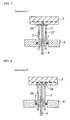
mounting structure in the wafer holder of the present invention;
Fig. 6 is a schematic sectional view depicting another specific example of
a mounting structure in the wafer holder of the present invention;
Fig. 7 is a schematic sectional view depicting a further specific example
of a mounting structure in the wafer holder of the present invention;
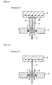
Fig. 8 is a schematic sectional view depicting yet another specific
example of a mounting structure in the wafer holder of the present invention;
Fig. 9 is a schematic sectional view depicting still another specific
example of a mounting structure in the wafer holder of the present invention;
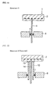
Fig. 10 is a schematic sectional view depicting a further specific example
of a mounting structure in the wafer holder of the present invention;
Fig. 11 is a schematic sectional view depicting yet another specific
example of a mounting structure in the wafer holder of the present invention;
and
Fig. 12 is a schematic sectional view depicting a specific example of a
mounting structure in a conventional wafer holder.
Best Mode for Carrying Out the Invention
In accordance with the present invention, as illustrated in Fig. 1 for
example, in a wafer holder 1 having a ceramic substrate 2 in which an electric
circuit such as a resistive heating element 3 is embedded, leads 4 for connecting
to external electrodes for supplying power to the resistive heating element 3 or
the like are housed in tubular guide members 5, and the guide members 5 are
installed penetrating the reaction chamber 6. One end of each guide member 5
is not joined to the ceramic substrate 2, and the other end thereof is
hermetically plugged at the reaction chamber 6 by means of an O-ring 7 or the
like, and at the same time a hermetic plug is also formed within the interior of
the guide member 5. It should be understood that reference numeral 8 in Fig. 1
denotes a water-cooling device provided in a bottom wall of the reaction
chamber 6.
In contrast, as illustrated in Fig. 12, in the structure set out in the
previously-mentioned Japanese Pat. Pub. No. 2525974, a tubular piece 15 that
houses a lead 14 is joined gastight to the ceramic substrate 12 by means of a
glass joint 19, and also sealed hermetically at the reaction chamber 6 by means
of an O-ring 7. As a consequence, the interior of the tubular piece 15 is the air at
atmospheric pressure, allowing heat to dissipate through the air at atmospheric
pressure within the tubular piece 15 and compromising the temperature
uniformity of the wafer holder.
In contrast to the conventional structure, the above-described wafer
holder 1 of the present invention, having the structure as illustrated in Fig. 1,
enables the atmosphere near the ceramic substrate 2 within the
internally-plugged guide member 5 to be substantially the same as the
atmosphere within the reaction chamber 6. This allows the heat escaping
through the atmosphere within the tubular guide member 5 to be remarkably
less than is conventional. Furthermore, since the guide member 5 is not joined
to the ceramic substrate 2, the amount of heat conducted to the guide member 5
is also reduced. These effects make it possible to enhance the temperature
uniformity of the wafer holder 1.
What is more, as noted above, the interior of the guide member 5 toward
the ceramic substrate 2 is substantially the same as the atmosphere within the
reaction chamber 6 at all times and does not allow the entry of ambient air.
Therefore, the high-temperature portions of the electrode terminals and the
leads 4 are shielded from the atmosphere, making their deterioration due to
oxidation unlikely to occur and leading to extended lifetime. In addition, since
the guide member 5 is not joined to the ceramic substrate 2, elevated costs due
to reduction in throughput in jointing, as was conventionally the case.
When the lead 4 is housed in the tubular guide member 5 in this way, it is
preferable that a portion of or the entirety of the lead 4 where it is disposed in
the reaction chamber 6 be covered by the guide member 5. In particular, if the
distances between a plurality of electrode terminals or leads 4 provided in the
ceramic substrate 2 are short, sparks are liable to be generated due to their
potential differences, but even in such cases, it is possible to suppress the
generation of sparks by housing a large portion of or the entirety of the lead 4
that is within the reaction chamber 6 into an insulative guide member 5.
In the present invention, it is also possible to join one end of the guide
member to the ceramic substrate, and such cases will be described later. In
cases where the reaction chamber is an insulator such as alumina or cordierite,
there is no possibility of current leakage to the reaction chamber side; therefore,
for example as illustrated in Fig. 11, it is possible to hermetically seal the
interval between the lead 4 and the reaction chamber 6 directly by means of an
O-ring 7 or the like, without using an insulative guide member. In this case as
well, it is possible to install a guide member in the reaction chamber to cover a
portion of the lead as needed.
Next, with regard to insulative guide members that house leads, the
plugging configuration at the other end of the guide member shown in Fig. 1 is
described. First, it is necessary that the guide member 5 penetrate outside the
reaction chamber 6 along where the lead 4 penetrates the reaction chamber 6.
The reason for this is because the reaction chamber 6 is generally made of metal,
current leakage can be prevented if the insulative guide member 5 covers at
least the portion of the lead 4 where it penetrates the reaction chamber 6. Thus,
the interval between the guide member 5 and the reaction chamber 6 is
hermetically sealed by means of an O-ring 7 or the like.
At the same time, within the interior of the guide member 5 as well, the
interval between the guide member 5 and the lead 4 is hermetically plugged.
For this hermetic plugging within the guide member, it is preferable to use
glass or a brazing material. Because the temperature of the lead grows high due
to the heat transmitted from the ceramic substrate, plugging using glass, which
has heat resistance, is preferable in terms of reliability. Nevertheless, plugging
using an organic resin is also possible when, for example, the working
temperature is low. With regard to the plugging location within the guide
member, preferably it is plugged in a portion that is separated as far a distance
as possible from the ceramic substrate, in order to minimize corrosion of the
lead due to the atmosphere.
A specific hermetic plugging within the guide member is explained with
reference to the drawings. A preferable method is, as illustrated in Figs. 2 and 3,
that the inner circumference of the distal end of the guide member 5 is
machined to have a step and further, that the lead 4 is formed to have a
protuberance 4a shaped so as to fit into the step in the guide member 5. The
difference between the outer diameter of the protuberance 4a on the lead 4 and
the inner diameter of the guide member 5 preferably is as small as possible;
however, it is desirable that the difference be about 0.1 mm. A larger difference
in the inner diameters reduces throughput in plugging and is therefore
disadvantageous.
In the plugging method represented in Fig. 2, after inserting a lead 4 into
this guide member 5, injecting glass 21 onto the stepped portion, and placing a
ring-shaped member 22 thereon, a heating process is carried out at a
predetermined temperature to soften the glass 21, so that the protuberance 4a
from the lead 4, the guide member 5, and the ring-shaped member 22 are
bonded together to form a hermetical plug. The glass 21 here may be powder, or
may in advance be pre-baked or a molded piece. More reliable plugging is
possible if load is applied to the glass 21 during this process.
In the plugging method represented in Fig. 3, the lead 4 is inserted into a
guide member 5 that has been machined to have a step as in the case of Fig. 2,
and the protuberance 4a from the lead 4 and the guide member 5 are joined
together using a brazing material 23; thus, a hermetical plug is formed within
the guide member 5.
In addition, as illustrated in Fig. 4, it is also possible to form a hermetic
plug by inserting a heat-resistant resin 24 into the lead member 5 and joining
the lead 4 and the guide member 5 directly. In this case of joining by means of
resin, it is desirable that the plugging be in a location distant from the ceramic
substrate to prevent the temperature of the plugged portion from becoming
elevated. Specific methods of plugging within the guide member are not limited
to the foregoing methods, but any methods may be adopted insofar as hermetic
plugging is possible.
Next, a configuration for mounting the guide member to the ceramic
substrate is explained. In a preferable mounting structure, as illustrated in Fig.
5 for example, a tubular guide member 5 in which a lead 4 is housed
advantageously is not joined to the ceramic substrate 2 constituting the wafer
holder 1, but is spaced apart from the surface on the side (back side) of the
ceramic susceptor 2 opposite its wafer retaining surface. The reason is that
within the interior of the internally-plugged guide member 5, the atmosphere
toward the ceramic substrate 2 is thereby made substantially the same as the
atmosphere within the reaction chamber 6.
In addition, in cases where the voltage is high tension, the guide member
can be joined to the ceramic substrate in order to prevent sparking by ensuring
inter-terminal insulation between the electrodes provided in the ceramic
substrate. This makes it necessary, however, to implement a machining process
on the guide member in order to introduce inside it the atmosphere within the
reaction chamber. It will be appreciated that, in this case, almost the entirety or
the major portion of the lead should be housed in the guide member, but it is
also possible to house only that portion where the risk of sparking is greatest.
For example, as shown in Figs. 6 and 7, one end of the guide member 5
and the ceramic substrate 2 may be joined together with a joint part 25 utilizing
glass, a brazing material or the like. In this case, the atmosphere within the
guide member 5 is made substantially the same as the atmosphere within the
reaction chamber 6 by means of a piercing hole 26 bored in the guide member 5
in the case of Fig. 6, or by means of an assemblage 27 in which the guide
member 5 is pieced together with a plurality of parts.
As shown in Fig. 8, one way the guide member and the ceramic substrate
may be joined is to anchor them by means of a screw joint 28 in which a screw
hole is formed in the back side of the ceramic substrate 2, and into the screw
hole, an end of the guide member 5 that has been machined into a screw is
screwed. In this case as well, it is desirable to form a piercing hole 26 in the
guide member 5 in order to make the atmospheres same within the guide
member 5 and the reaction chamber 6.
In cases where the guide member is joined to the ceramic substrate, it is
possible to prevent the escaping heat through the atmosphere within the guide
member 5 and eliminate oxidation of the lead 4 without forming a piercing hole
or the like in the guide member if within the hermetically-plugged guide
member 5 the atmosphere A as indicated in Fig. 9 on the ceramic substrate 2
side of the plug is made a vacuum. Alternatively, in cases where sparking
between the electrodes or leads provided in the ceramic substrate is unlikely to
occur, such as where the working voltage is low, it is possible to arrange the
guide member 5 only along the portion of the lead 4 where it penetrates the
reaction chamber 6, as shown in Fig. 10.
While there are no particular restrictions as to the material for the guide
member used in the present invention, inorganic ceramics, glass, and
heat-resistant organic resins may be used. These materials may be selected
according to how the wafer holder is employed. Preferable among ceramics are
those whose chief component is whichever of mullite, alumina, silicon nitride,
silicon carbide, or aluminum nitride.
When the guide member is installed either joined to or in contact with
the ceramic substrate, it is desirable that the thermal conductivity of the guide
member be lower than that of the ceramic substrate. This is because the heat
generated by the resistive heating element diffuses into the ceramic substrate,
and under the circumstances, if the thermal conductivity of the guide member
is higher than that of the ceramic substrate, the heat generated by the resistive
heating element will diffuse into the guide member before it uniformly diffuses
through the ceramic substrate, lowering the temperature of the substrate area
in contact with the guide members compared with the temperature of the rest of
the substrate and consequently making the temperature distribution of the
wafer retaining surface non-uniform.
In view of this, it is preferable that the thermal conductivity of the guide
member be as low as possible. In addition, in cases where the guide member is
joined to the ceramic substrate, it is preferable that its thermal expansion
coefficient be near that of the ceramic substrate in order to reduce the stress
incidents of at the joint. Taking these points into consideration, mullite is
particularly preferable as the substance of the guide member for its having a
very low thermal conductivity of about 1 W/mk, and also having a thermal
expansion coefficient of 4 to 6 × 10⁻⁶/K, which is closely akin to those of general
ceramics.
Although it does not particularly matter what the substance of the
ceramic susceptor is, preferable is one in which the principal component is
whichever of alumina, silicon nitride, aluminum nitride, and silicon carbide.
Because demands for uniformization of temperature distribution in wafer
holders have grown intense in recent years, materials of high conductivity are
preferable. Specifically, aluminum nitride and silicon carbide, which exhibit a
thermal conductivity of higher than 100 W/mk, are preferable, with aluminum
nitride being particularly preferable owing to the superiority of its corrosion
resistance and insulating properties.
Meanwhile silicon nitride, because the strength of the ceramic itself at
elevated temperatures is high compared with other ceramics, is ideal
particularly for susceptors employed at high temperatures. Another advantage
of the three substances, namely, silicon nitride, aluminum nitride, and silicon
carbide, is their superior resistance to thermal shock, such that these ceramics
are capable of rapid rise and fall in temperature. Alumina stands out
meanwhile in that from a cost aspect it is superior compared with the other
three ceramics. The choice as to which of these ceramics to use will as a matter
of course depend on the application.
The wafer holder of the present invention, with incorporating a resistive
heating element, a plasma-generating electrode, an electrostatic chuck
electrode, an electron-beam electrode or the like according to the application,
can be suitably installed in the reaction chambers of a variety of semiconductor
manufacturing apparatuses. Most especially, the superior temperature
uniformity of the wafer retaining surface means that the temperature
distribution of the wafer is made exceedingly uniform during every sort of
process, such as CVD and etching.
Additionally, in the wafer holder of the present invention, since the
electrodes and the leads are generally exposed to the atmosphere within the
reaction chamber, it is preferable that the gas used in the reaction chamber not
be corrosive gases. For this reason, among semiconductor manufacturing
apparatuses, use in an apparatus for low-k film baking, which does not have
many restrictions on the materials that can be inserted into the reaction
chamber, is especially suitable. Because the apparatus for low-k film baking
does not use a corrosive gas, it is unnecessary to take corrosion of electrode
terminals and leads, as well as of guide members, into consideration.
Embodiments
Embodiment 1
Slurries were prepared by adding predetermined amounts of sintering
additive, binder, solvent, and so forth to ceramic powders of AIN, Si3N4, Al2O3,
and SiC and blending the mixture with a ball mill. These slurries were
granulated by spray drying, and the obtained granules were press-molded
using dies of predetermined form. The molded objects thus produced were
degreased and then sintered at respective predetermined temperatures, and
ceramic substrates were obtained.
Using a technique such as screen printing, a resistive heating element
circuit was formed on the ceramic substrates thus obtained, as well as RF
electrodes, electrostatic-chuck electrodes, or electron-beam electrodes as needed.
Each printed substrate was baked under predetermined conditions, and a
ceramic plate was bonded over the substrate to cover the resistive heating
element, RF electrodes, and electrostatic-chuck electrodes in order to protect
them as needed. A wafer pocket for carrying a wafer was formed in the
substrate by a machining operation, and electrode terminals and leads for
connecting to the electric circuits were installed.
Meanwhile, guide members for housing electrode terminals and leads
were fabricated from the base-material ceramics set forth in Tables I to IV.
Prepared were simple tubular guide members, as well as guide members in
which, to accord with the ceramic-substrate-end mounting structures A to G
and Z shown in Figs. 5 to 12, piercing holes were formed and in which a
plurality of parts were pieced together. Here, all the guide members had an
outer diameter of 10 mm and an inner diameter of 6 mm.
Next, these guide members were attached to a side of each ceramic
substrate in accordance with Structures A to G and Z shown in Figs. 5 to 12.
Specifically, the guide members used were: tubular guide members that have
not machined for Structures A, E, F, and Z; guide members having a 2
mm-diameter piercing holes for Structures B and D; and a guide member in
which a plurality of parts are pieced together, for Structure C. To join the guide
members and the ceramic substrates, screw-joining by means of screws was
employed for Structure D, whereas glass was used for the others. However,
Structure G did not use a guide member.
Thereafter, the interior of each guide member that housed a lead was
hermetically plugged. Specifically, for the glass plug, plugging was in the
manner shown in Fig. 2 using a glass ceramic; for the braze-material plug,
plugging was in the manner shown in Fig. 3 using an active metal brazing
material; and for the resin plug, plugging was in the manner shown in Fig. 4
using a heat-resistant epoxy resin. For Structure E, plugging was done in a
vacuum so that the interior of the guide member would be a vacuum. Each of
the internally-plugged guide members was penetrated at a predetermined
location through a reaction chamber made of aluminum or alumina, having a
predetermined configuration, and the interval between the reaction chamber
and the guide member was hermetically plugged by means of an O-ring. In
Structure G, which does not use a guide member, the interval between the
reaction chamber and the lead was hermetically sealed directly by means of an
O-ring.
With each sample wafer holder thus configured, electric current was
passed through the resistive heating element to raise the temperature to the
heater temperatures set forth in Tables I to IV with an inert gas being
introduced into the reaction chamber, and the temperature uniformity was
found by measuring the temperature of the wafer retaining surface with a
wafer temperature gauge; the results obtained are set forth in the following
Tables I to IV Thereafter, each sample was cooled to room temperature, and the
degrees of oxidation of the leads were evaluated. The results are shown in
Tables I to IV, wherein those that exhibited almost no change in their surface
color are indicated as "good," those with a slight color change into blue as "fair,"
and those with a color change into yellow as "poor." In all the samples, the lead
material was a 4 mm diameter material of tungsten.
| Ceramic substrate: AlN |
| Sample | Guide member | Reaction chamber | Heater temp (°C) | Internal plug | Mounting Struct. | Temp. uniformity (%) | Lead oxidation |
| 1 | Mullite | Al | 500 | Glass plug | Struct. A | ±0.3 | Good |
| 2 | Mullite | Al | 850 | Glass plug | Struct. A | ±0.3 | Good |
| 3 | Mullite | Al | 850 | Brazing material plug | Struct. A | ±0.3 | Good |
| 4 | Mullite | Al | 850 | Glass plug | Struct. B | ±0.4 | Good |
| 5 | Mullite | Al | 850 | Glass plug | Struct. C | ±0.4 | Good |
| 6 | Mullite | Al | 850 | Glass plug | Struct. D | ±0.4 | Good |
| 7 | Mullite | Al | 850 | Brazing plug material plug | Struct. E | ±0.4 | Good |
| 8 | Mullite | Al | 850 | Glass plug | Struct. F | ±0.3 | Good |
| 9 | Mullite | Al | 500 | Resin | Struct. F | ±0.3 | Good |
| 10 | None | Al2O3 | 500 | N/A | Struct. G | ±0.3 | Good |
| 11* | Mullite | Al | 500 | None | Struct. Z | ±0.6 | Fair |
| 12* | Mullite | Al | 850 | None | Struct. Z | ±0.6 | Poor |
| 13 | Mullite-Al2O3 | Al | 500 | Glass plug | Struct. A | ±0.3 | Good |
| 14 | Mullite- Al2O3 | Al | 850 | Glass plug | Struct. A | ±0.3 | Good |
| 15 | Mullite- | Al | 850 | Glass plug | Struct. C | ±0.4 | Good |
| 16* | Mullite-Al2O3 | Al | 850 | None | Struct. Z | ±0.6 | Poor |
| 17 | Al2O3 | Al | 500 | Glass plug | Struct. A | ±0.3 | Good |
| 18 | Al2O3 | Al | 850 | Glass plug | Struct. A | ±0.3 | Good |
| 19 | Al2O3 | Al | 850 | Glass plug | Struct. C | ±0.4 | Good |
| 20* | Al2O3 | Al | 850 | None | Struct. Z | ±0.6 | Poor |
| 21 | Si3N4 | Al | 500 | Glass plug | Struct. A | ±0.3 | Good |
| 22 | Si3N4 | Al | 850 | Glass plug | Struct. A | ±0.3 | Good |
| 23 | Si3N4 | Al | 850 | Glass plug | Struct. B | ±0.4 | Good |
| 24* | Si3N4 | Al | 850 | None | Struct. Z | ±0.6 | Poor |
| 25 | Sic | Al | 500 | Glass plug | Struct. A | ±0.3 | Good |
| 26 | Sic | Al | 850 | Glass plug | Struct. A | ±0.3 | Good |
| 27 | Sic | Al | 850 | Glass plug | Struct. B | ±0.5 | Good |
| 28* | Sic | Al | 850 | None | Struct. Z | ±0.7 | Poor |
| 29 | AlN | Al | 500 | Glass plug | Struct. A | ±0.4 | Good |
| 30 | AlN | Al | 850 | Glass plug | Struct. A | ±0.4 | Good |
| 31 | AlN | Al | 850 | Glass plug | Struct. C | ±0.5 | Good |
| 32* | AlN | Al | 850 | None | Struct. Z | ±0.7 | Poor |
| (Note) Samples marked with an asterisk (*) in the table are comparative examples. |
| Ceramic substrate: Si3N4 |
| Sample | Guide member | Reaction chamber | Heater temp. (°C) | Internal plug | Mounting struct. | Temp. uniformity (%) | Lead oxidation |
| 1 | Mullite | Al | 500 | Glass | Struct. A | ±0.5 | Good |
| 2 | Mullite | Al | 850 | Glass plug | Struct. A | ±0.5 | Good |
| 3 | Mullite | Al | 1100 | Glass plug | Struct. A | ±0.5 | Good |
| 4 | Mullite | Al | 850 | Brazing material plug | Struct. A | ±0.5 | Good |
| 5 | Mullite | Al | 850 | Glass plug | Struct. B | ±0.6 | Good |
| 6 | Mullite | Al | 850 | Glass plug | Struct. C | ±0.6 | Good |
| 7 | Mullite | Al | 850 | Glass plug | Struct. D | ±0.6 | Good |
| 8 | Mullite | Al | 850 | Brazing plug material plug | Struct. E | ±0.6 | Good |
| 9 | Mullite | Al | 850 | Glass plug | Struct. F | ±0.5 | Good |
| 10 | Mullite | Al | 500 | Resin | Struct. F | ±0.5 | Good |
| 11 | None | Al2O3 | 500 | N/A | Struct. G | ±0.5 | Good |
| 12* | Mullite | Al | 500 | None | Struct. Z | ±1.3 | Fair |
| 13* | Mullite | Al | 850 | None | Struct. Z | ±1.3 | Poor |
| 14 | Mullite-Al2O3 | Al | 500 | Glass plug | Struct. A | ±0.5 | Good |
| 15 | Mullite-Al2O3 | Al | 850 | Glass plug | Struct. A | ±0.5 | Good |
| 16 | Mullite- | Al | 1100 | Glass plug | Struct. A | ±0.5 | Good |
| 17 | Mullite-Al2O3 | Al | 850 | Glass plug | Struct. C | ±0.6 | Good |
| 18* | Mullite-Al2O3 | Al | 850 | None | Struct. Z | ±L.3 | Poor |
| 19 | Al2O3 | Al | 500 | Glass plug | Struct. A | ±0.5 | Good |
| 20 | Al2O3 | Al | 850 | Glass plug | Struct. A | ±0.5 | Good |
| 21 | Al2O3 | Al | 1100 | Glass plug | Struct. A | ±0.5 | Good |
| 22 | Al2O3 | Al | 850 | Glass plug | Struct. C | ±0.6 | Good |
| 23* | Al2O3 | Al | 850 | None | Struct. Z | ±1.3 | Poor |
| 24 | Si3N4 | Al | 500 | Glass plug | Struct. A | ±0.5 | Good |
| 25 | Si3N4 | Al | 850 | Glass plug | Struct. A | ±0.5 | Good |
| 26 | Si3N4 | Al | 850 | Glass plug | Struct. B | ±0.6 | Good |
| 27* | Si3N4 | Al | 850 | None | Struct. Z | ±1.3 | Poor |
| 28 | Sic | Al | 500 | Glass plug | Struct. A | ±0.5 | Good |
| 29 | Sic | Al | 850 | Glass plug | Struct. A | ±0.5 | Good |
| 30 | Sic | Al | 850 | Glass plug | Struct. B | ±0.5 | Good |
| 31* | Sic | Al | 850 | None | Struct. Z | ±1.5 | Poor |
| 32 | AlN | Al | 500 | Glass plug | Struct. A | ±0.6 | Good |
| 33 | AlN | Al | 850 | Glass plug | Struct. A | ±0.6 | Good |
| 34 | AlN | Al | 850 | Glass plug | Struct. C | ±0.5 | Good |
| 35* | AlN | Al | 850 | None | Struct. Z | ±1.5 | Poor |
| (Note) Samples marked with an asterisk (*) in the table are comparative examples. |
| Ceramic substrate: Al2O3 |
| Sample | Guide member | Heater Reaction chamber temp. (°C) | Internal plug | Mounting struct. | Temp. uniformity (%) | Lead oxidation |
| 1 | Mullite | Al | 500 | Glass plug seal | Struct. A | ±0.5 | Good |
| 2 | Mullite | Al | 850 | Glass plug | Struct. A | ±0.5 | Good |
| 3 | Mullite | Al | 850 | Brazing material plug | Struct. A | ±0.5 | Good |
| 4 | Mullite | Al | 850 | Glass plug | Struct. B | ±0.6 | Good |
| 5 | Mullite | Al | 850 | Glass plug | Struct. C | ±0.6 | Good |
| 6 | Mullite | Al | 850 | Glass plug | Struct. D | ±0.6 | Good |
| 7 | Mullite | Al | 850 | Brazing material plug | Struct. E | ±0.6 | Good |
| 8 | Mullite | Al | 850 | Glass plug | Struct. F | ±0.5 | Good |
| 9 | Mullite | Al | 500 | Resin plug | Struct. F | ±0.5 | Good |
| 10 | None | Al2O3 | 500 | N/A | Struct. G | ±0.5 | Good |
| 11* | Mullite | Al | 500 | None | Struct. Z | ±1.3 | Fair |
| 12* | Mullite | Al | 850 | None | Struct. Z | ±1.3 | Poor |
| 13 | Mullite-Al2O3 | Al | 500 | Glass plug | Struct. A | ±0.5 | Good |
| 14 | Mullite-Al2O3 | Al | 850 | Glass plug | Struct. A | ±0.5 | Good |
| 15 | Mullite- | Al | 850 | Glass plug | Struct. C | ±0.6 | Good |
| 16* | Mullite- | Al | 850 | None | Struct. Z | ±1.3 | Poor |
| 17 | Al2O3 | Al | 500 | Glass plug | Struct. A | ±0.5 | Good |
| 18 | Al2O3 | Al | 850 | Glass plug | Struct. A | ±0.5 | Good |
| 19 | Al2O3 | Al | 850 | Glass plug | Struct. C | ±0.6 | Good |
| 20* | Al2O3 | Al | 850 | None | Struct. Z | ±1.3 | Poor |
| 21 | Si3N4 | Al | 500 | Glass plug | Struct. A | ±0.5 | Good |
| 22 | Si3N4 | Al | 850 | Glass plug | Struct. A | ±0.5 | Good |
| 23 | Si3N4 | Al | 850 | Glass plug | Struct. B | ±0.6 | Good |
| 24* | Si3N4 | Al | 850 | None | Struct. Z | ±1.3 | Poor |
| 25 | SiC | Al | 500 | Glass plug | Struct. A | ±0.5 | Good |
| 26 | SiC | Al | 850 | Glass plug | Struct. A | ±0.5 | Good |
| 27 | SiC | Al | 850 | Glass plug | Struct. B | ±0.5 | Good |
| 28* | SiC | Al | 850 | None | Struct. Z | ±1.5 | Poor |
| 29 | AlN | Al | 500 | Glass plug | Struct. A | ±0.6 | Good |
| 30 | AIN | Al | 850 | Glass plug | Struct. A | ±0.6 | Good |
| 31 | AlN | Al | 850 | Glass plug | Struct. C | ±0.5 | Good |
| 32* | AlN | Al | 850 | None | Struct. Z | ±1.5 | Poor |
| (Note) Samples marked with an asterisk (*) in the table are comparative examples. |
| Ceramic substrate: SiC |
| Sample | Guide member | Reaction chamber | Heater temp. (°C) | Internal plug | Mounting struct. | Temp. uniformity (%) | Lead oxidation |
| 1 | Mullite | Al | 500 | Glass plug | Struct. A | ±0.3 | Good |
| 2 | Mullite | Al | 850 | Glass plug | Struct. A | ±0.3 | Good |
| 3 | Mullite | Al | 850 | Brazing plug material plug | Struct. A | ±0.3 | Good |
| 4 | Mullite | Al | 850 | Glass plug | Struct. B | ±0.4 | Good |
| 5 | Mullite | Al | 850 | Glass plug | Struct. C | ±0.3 | Good |
| 6 | Mullite | Al | 850 | Glass plug | Struct. D | ±0.4 | Good |
| 7 | Mullite | Al | 850 | Brazing material plug | Struct. E | ±0.4 | Good |
| 8 | Mullite | Al | 850 | Glass plug | Struct. F | ±0.3 | Good |
| 9 | Mullite | Al | 500 | Resin plug | Struct. F | ±0.3 | Good |
| 10 | None | Al2O3 | 500 | N/A | Struct. G | ±0.3 | Good |
| 11* | Mullite | Al | 500 | None | Struct. Z | ±0.6 | Fair |
| 12* | Mullite | Al | 850 | None | Struct. Z | ±0.6 | Poor |
| 13 | Mullite- Al2O3 | Al | 500 | Glass plug | Struct. A | ±0.3 | Good |
| 14 | Mullite- Al2O3 | Al | 850 | Glass plug | Struct. A | ±0.3 | Good |
| 15 | Mullite- Al2O3 | Al | 850 | Glass plug | Struct. C | ±0.3 | Good |
| 16* | Mullite-Al2O3 | Al | 850 | None | Struct. Z | ±0.6 | Poor |
| 17 | Al2O3 | Al | 500 | Glass plug | Struct. A | ±0.3 | Good |
| 18 | Al2O3 | Al | 850 | Glass plug | Struct. A | ±0.3 | Good |
| 19 | Al2O3 | Al | 850 | Glass plug | Struct. C | ±0.3 | Good |
| 20* | Al2O3 | Al | 850 | None | Struct. Z | ±0.6 | Poor |
| 21 | Si3N4 | Al | 500 | Glass plug | Struct. A | ±0.3 | Good |
| 22 | Si3N4 | Al | 850 | Glass plug | Struct. A | ±0.3 | Good |
| 23 | Si3N4 | Al | 850 | Glass plug | Struct. B | ±0.4 | Good |
| 24* | Si3N4 | Al | 850 | None | Struct. Z | ±0.6 | Poor |
| 25 | SiC | Al | 500 | Glass plug | Struct. A | ±0.3 | Good |
| 26 | SiC | Al | 850 | Glass plug | Struct. A | ±0.3 | Good |
| 27 | SiC | Al | 850 | Glass plug | Struct. B. | ±0.5 | Good |
| 28* | SiC | Al | 850 | None | Struct. Z | ±0.7 | Poor |
| 29 | AlN | Al | 500 | Glass plug | Struct. A | ±04 | Good |
| 30 | AlN | Al | 850 | Glass plug | Struct. A | ±0.4 | Good |
| 31 | AlN | Al | 850 | Glass plug | Struct. C | ±0.5 | Good |
| 32* | AlN | Al | 850 | None | Struct. Z | ±0.7 | Poor |
| (Note) Samples marked with an asterisk (*) in the table are comparative examples. |
As will be understood from the results noted above, the wafer holders of
the present invention, in which the guide members were hermetically plugged
along the interior, achieved superior temperature uniformities in any of
Structures A to G, compared with the wafer holder of Structure Z (Fig. 12), in
which a conventional guide member is used. Moreover, the conventional wafer
holder of Structure Z oxidation of the leads was evident, whereas with every
sample of the present invention no oxidation of the leads was at all discernible.
Embodiment 2
Each sample wafer holder of the present invention fabricated according
to Embodiment 1 was installed in a low-k film baking apparatus to process a
wafer. The results were that all the wafer holders were capable of performing
low-k film baking appropriately, and in particular, the wafer holders that
exhibited a temperature uniformity of less than 0.5% yielded excellent film
quality.
Industrial Applicability
The present invention provides wafer holders in which local heat
radiation during heating is kept under control and temperature uniformity of
the wafer retaining surface is enhanced. Accordingly, using the wafer holders
makes it possible to provide semiconductor manufacturing apparatuses that
have high temperature uniformity, superior durability of electrode terminals
and leads and are suitable for processing larger-diameter wafers.