JP3832409B2 - Wafer holder and semiconductor manufacturing apparatus - Google Patents
Wafer holder and semiconductor manufacturing apparatus Download PDFInfo
- Publication number
- JP3832409B2 JP3832409B2 JP2002270951A JP2002270951A JP3832409B2 JP 3832409 B2 JP3832409 B2 JP 3832409B2 JP 2002270951 A JP2002270951 A JP 2002270951A JP 2002270951 A JP2002270951 A JP 2002270951A JP 3832409 B2 JP3832409 B2 JP 3832409B2
- Authority
- JP
- Japan
- Prior art keywords
- guide member
- wafer holder
- reaction vessel
- ceramic substrate
- lead
- Prior art date
- Legal status (The legal status is an assumption and is not a legal conclusion. Google has not performed a legal analysis and makes no representation as to the accuracy of the status listed.)
- Expired - Fee Related
Links
Images


Classifications
-
- H—ELECTRICITY
- H01—ELECTRIC ELEMENTS
- H01L—SEMICONDUCTOR DEVICES NOT COVERED BY CLASS H10
- H01L21/00—Processes or apparatus adapted for the manufacture or treatment of semiconductor or solid state devices or of parts thereof
- H01L21/02—Manufacture or treatment of semiconductor devices or of parts thereof
-
- H—ELECTRICITY
- H01—ELECTRIC ELEMENTS
- H01L—SEMICONDUCTOR DEVICES NOT COVERED BY CLASS H10
- H01L21/00—Processes or apparatus adapted for the manufacture or treatment of semiconductor or solid state devices or of parts thereof
- H01L21/67—Apparatus specially adapted for handling semiconductor or electric solid state devices during manufacture or treatment thereof; Apparatus specially adapted for handling wafers during manufacture or treatment of semiconductor or electric solid state devices or components ; Apparatus not specifically provided for elsewhere
- H01L21/683—Apparatus specially adapted for handling semiconductor or electric solid state devices during manufacture or treatment thereof; Apparatus specially adapted for handling wafers during manufacture or treatment of semiconductor or electric solid state devices or components ; Apparatus not specifically provided for elsewhere for supporting or gripping
- H01L21/687—Apparatus specially adapted for handling semiconductor or electric solid state devices during manufacture or treatment thereof; Apparatus specially adapted for handling wafers during manufacture or treatment of semiconductor or electric solid state devices or components ; Apparatus not specifically provided for elsewhere for supporting or gripping using mechanical means, e.g. chucks, clamps or pinches
- H01L21/68714—Apparatus specially adapted for handling semiconductor or electric solid state devices during manufacture or treatment thereof; Apparatus specially adapted for handling wafers during manufacture or treatment of semiconductor or electric solid state devices or components ; Apparatus not specifically provided for elsewhere for supporting or gripping using mechanical means, e.g. chucks, clamps or pinches the wafers being placed on a susceptor, stage or support
- H01L21/68757—Apparatus specially adapted for handling semiconductor or electric solid state devices during manufacture or treatment thereof; Apparatus specially adapted for handling wafers during manufacture or treatment of semiconductor or electric solid state devices or components ; Apparatus not specifically provided for elsewhere for supporting or gripping using mechanical means, e.g. chucks, clamps or pinches the wafers being placed on a susceptor, stage or support characterised by a coating or a hardness or a material
-
- H—ELECTRICITY
- H01—ELECTRIC ELEMENTS
- H01L—SEMICONDUCTOR DEVICES NOT COVERED BY CLASS H10
- H01L21/00—Processes or apparatus adapted for the manufacture or treatment of semiconductor or solid state devices or of parts thereof
- H01L21/67—Apparatus specially adapted for handling semiconductor or electric solid state devices during manufacture or treatment thereof; Apparatus specially adapted for handling wafers during manufacture or treatment of semiconductor or electric solid state devices or components ; Apparatus not specifically provided for elsewhere
- H01L21/67005—Apparatus not specifically provided for elsewhere
- H01L21/67011—Apparatus for manufacture or treatment
- H01L21/67098—Apparatus for thermal treatment
- H01L21/67103—Apparatus for thermal treatment mainly by conduction
-
- H—ELECTRICITY
- H01—ELECTRIC ELEMENTS
- H01L—SEMICONDUCTOR DEVICES NOT COVERED BY CLASS H10
- H01L21/00—Processes or apparatus adapted for the manufacture or treatment of semiconductor or solid state devices or of parts thereof
- H01L21/67—Apparatus specially adapted for handling semiconductor or electric solid state devices during manufacture or treatment thereof; Apparatus specially adapted for handling wafers during manufacture or treatment of semiconductor or electric solid state devices or components ; Apparatus not specifically provided for elsewhere
- H01L21/67005—Apparatus not specifically provided for elsewhere
- H01L21/67242—Apparatus for monitoring, sorting or marking
- H01L21/67248—Temperature monitoring
-
- H—ELECTRICITY
- H01—ELECTRIC ELEMENTS
- H01L—SEMICONDUCTOR DEVICES NOT COVERED BY CLASS H10
- H01L21/00—Processes or apparatus adapted for the manufacture or treatment of semiconductor or solid state devices or of parts thereof
- H01L21/67—Apparatus specially adapted for handling semiconductor or electric solid state devices during manufacture or treatment thereof; Apparatus specially adapted for handling wafers during manufacture or treatment of semiconductor or electric solid state devices or components ; Apparatus not specifically provided for elsewhere
- H01L21/68—Apparatus specially adapted for handling semiconductor or electric solid state devices during manufacture or treatment thereof; Apparatus specially adapted for handling wafers during manufacture or treatment of semiconductor or electric solid state devices or components ; Apparatus not specifically provided for elsewhere for positioning, orientation or alignment
Description
【0001】
【発明の属する技術分野】
本発明は、半導体製造工程においてウエハーを加熱し、所定の処理を行うためのウエハー保持体、及びそのウエハー保持体を供えた半導体製造装置に関するものである。
【0002】
【従来の技術】
従来から、半導体製造装置に使用されるウエハー保持体に関して種々の構造が提案なされている。例えば、特公平6−28258号公報には、抵抗発熱体が埋設され、反応容器内に設置されたセラミックス製のヒータ部と、このヒータ部のウエハー加熱面以外の面に設けられ、反応容器との間で気密性シールを形成する凸状支持部と、前記抵抗発熱体に接続され、反応容器の内部空間に実質的に露出しないように容器外へ取り出された電極とを有する半導体ウエハー加熱装置が提案されている。
【0003】
また、特許第2525974号公報には、上記特公平6−28258号公報記載のセラミックスヒータ部(ウエハー保持体)に、筒状体を接合した構造が提案されている。即ち、セラミックスヒータ部と、このセラミックスヒータ部を保持するために反応容器内に設置された保持部材と、ヒータ端子に連結されたリードとを有する半導体ウエハー加熱装置であって、リードの少なくとも一つを無機質絶縁材料からなる筒状体によって包囲し、この筒状体の一端をセラミックスヒータに対して気密に接合し、且つ筒状体の他端を反応容器に設けられた貫通孔に挿通して気密にシールしている。
【0004】
【発明が解決しようとする課題】
特に近年において、ウエハーの大口径化が進むとともに、ウエハー保持体に関してはウエハー保持面における温度分布の均一性が求められている。しかし、上記特公平6−28258号公報記載の装置では、ウエハー保持体であるセラミックスヒータ部が反応容器との間で気密性シールされた凸状支持部に支持され、反応容器外の大気に接しているため、大気側への放熱によってウエハー保持面の均熱性が損なわれるという欠点があった。
【0005】
上記特許第2525974号公報記載の構造においても、リードを収納した筒状体はセラミックスヒータ部に接合され且つ反応容器を挿通して容器と気密に封止されているため、必然的に筒状体内部は大気圧となる一方、反応容器内のウエハー処理雰囲気は減圧若しくは真空である。従って、筒状体内で大気圧の空気によって放散される熱量が他の部分に比較して大きくなり、その結果セラミックスヒータ部の筒状体との接合部分の温度が低下して、ウエハー保持面の均熱性が損なわれるという問題があった。また、筒状体がセラミックスヒータ部に接合されているため、この部分での熱の逃げが大きくなり、更にウエハ−保持面の均熱性が損なわれる結果となっていた。
【0006】
更には、セラミックスヒータ部に給電するためのリードは大気雰囲気に曝されると共に、セラミックスヒータ部の加熱によってリードのセラミックスヒータ部側の温度が高温になる。このため、高温になったリード部が、空気中の酸素の影響で腐食されやすいという問題もあった。また、筒状体をセラミックスヒータ部に接合し、且つ反応容器との間で気密封止するために、その接合歩留が低いことによってコストが上昇してしまうという問題も存在していた。
【0007】
本発明は、このような従来の事情に鑑み、反応容器内でウエハーを保持加熱する際の局所的な放熱を抑え、ウエハ−保持面の均熱性を高めたウエハー保持体を提供すること、及びこのウエハー保持体を用いて、大口径のウエハーの処理にも適した半導体製造装置を提供することを目的とする。
【0008】
【課題を解決するための手段】
上記目的を達成するため、本発明が提供するウェハー保持体は、セラミックス基体中に抵抗発熱体、プラズマ発生用電極、及び静電チャック用電極の少なくとも一つを有し、これらを外部電極に接続するためのリードが反応容器を貫通して設けられたウェハー保持体であって、前記リードを筒状のガイド部材内に収納し、該ガイド部材と反応容器の間及び該ガイド部材内部が気密封止されており、気密封止されたガイド部材内のセラミックス基体側の雰囲気が、反応容器内の雰囲気と実質的に同一であるか、又は真空状態であることを特徴とする。
【0009】
上記本発明のウエハー保持体においては、ガイド部材とセラミックス基体とが接合されていないことを特徴とする。また、ガイド部材内部の気密封止部において、リードがガラス又はロウ材でガイド部材に接合されていることが好ましい。更に、上記本発明のウエハー保持体では、反応容器内に配置されるリードの一部又は全部がガイド部材で覆われていることが好ましい。
【0011】
上記本発明のウエハー保持体においては、ガイド部材の主成分が、ムライト、アルミナ、窒化ケイ素、炭化ケイ素、窒化アルミニウムのいずれかであることが好ましい。一方、セラミックス基体の主成分は、アルミナ、窒化ケイ素、窒化アルミニウム、炭化ケイ素のいずれかであることが好ましい。
【0012】
本発明は、また、上記本発明のウエハー保持体が反応容器内に搭載されていることを特徴とする半導体製造装置を提供する。この本発明の半導体製造装置においては、反応容器内の雰囲気が腐食性ガスでなことが好ましい。また、この本発明の半導体製造装置は、Low−k膜焼成用として好適である。
【0013】
【発明の実施の形態】
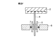
本発明において、例えば図1に示すように、セラミックス基体2中に抵抗発熱体3等の電気回路を埋設したウエハー保持体1では、抵抗発熱体3等に給電するため外部電極と接続されるリード4が筒状のガイド部材5内に収納され、そのガイド部材5は反応容器6を貫通して設置されている。また、ガイド部材5は、その一端をセラミックス基体2に接合せず、他端は反応容器6との間をO−リング7等で気密封止すると同時に、ガイド部材5の内部でも気密封止を施してある。尚、図1中の8は、反応容器6の底部壁に設けた水冷装置である。
【0014】
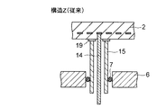
一方、上述した特許第2525974号公報記載の構造では、図12に示すように、リード14を収納した筒状体15はセラミックス基体12にガラス接合部19により気密に接合され、且つ反応容器6との間もO−リング7によって気密に封止されている。このため、筒状体15の内部は大気圧の空気となり、筒状体15内で大気圧の空気によって熱が放散され、ウエハー保持体の均熱性が低下していた。
【0015】
このような従来の構造に対して、上記した図1に示すような構造を有する本発明のウエハー保持体1では、内部封止されたガイド部材5内のセラミックス基体2側の雰囲気を、反応容器6内の雰囲気と実質的に同一にすることができる。このため、筒状のガイド部材5内の雰囲気からの熱の逃げを、従来に比較して格段に小さくすることができる。更に、ガイド部材5がセラミックス基体2に接合されていなため、ガイド部材5に伝達される熱も少なくすることができる。このような効果によって、ウエハー保持体1の均熱性を高めることができる。
【0016】
また、上記のごとくガイド部材5内のセラミックス基体2側は、常に反応容器6内の雰囲気と実質的に同一になり、大気雰囲気が侵入することがない。このため、電極端子やリード4の高温部が大気から遮断され、酸化による劣化が起こり難くなり、寿命を延ばすことができる。更に、ガイド部材5をセラミックス基体2に接合しないため、従来のような接合歩留の低下によるコスト上昇もなくなる。
【0017】
このように筒状のガイド部材5内にリード4を収納する場合、反応容器6内に配置されるリード4の一部又は全部をガイド部材5で覆うことが好ましい。特にセラミックス基体2に設けた複数の電極端子やリード4の間のそれぞれの距離が短いと、その電位差によってスパークが発生しやすいが、その場合でも反応容器6内のリード4の全部又は大部分を絶縁性のガイド部材5内に収納することによって、スパークの発生を抑えることが可能である。
【0018】
尚、本発明においては、ガイド部材の一端をセラミックス基体に接合することも可能であるが、その場合については後述する。また、反応容器がアルミナやコージェライトのような絶縁体である場合、反応容器側へ漏電する可能性がないため、絶縁性のガイド部材を用いることなく、例えば図11に示すように、リード4と反応容器6の間をO−リング7等で直接に気密封止することが可能である。この場合にも、必要に応じて、ガイド部材を反応容器内に取り付けて、リードの一部を覆うことも可能である。
【0019】
次に、リードを収納する絶縁性のガイド部材に関して、図1に示すガイド部材の他端における封止部構造について説明する。まず、リード4が反応容器6を貫通する部分で、ガイド部材5は反応容器6の外側に突き抜けていることが必要である。一般に反応容器6は金属製であるため、少なくとも反応容器6を貫通する部分のリード4を絶縁性のガイド部材5で覆うことによって、漏電を防ぐことができるからである。そして、そのガイド部材5と反応容器6の間は、O−リング7等で気密封止する。
【0020】
それと同時に、ガイド部材5の内部においても、ガイド部材5とリード4の間で気密封止を行う。このガイド部材内での気密封止には、ガラス又はロウ材を使用することが好ましい。リードはセラミックス基体から伝わる熱で高温になるため、耐熱性を有するガラスを用いて封止することが信頼性の点で好ましい。ただし、使用温度が低い場合などには、有機樹脂を用いて封止することも可能である。また、ガイド部材内での封止位置に関しては、リードの大気による腐食を最小限にするため、できるだけセラミックス基体から距離の離れた部分で封止することが好ましい。
【0021】
具体的なガイド部材内での気密封止について、図面を参照して説明する。好ましい方法としては、図2及び図3に示すように、ガイド部材5の他端内周側に段差加工を施し、更にリード4にはガイド部材5の段差に入り込む形の凸部4aを形成する。このときリード4の外径とガイド部材5の段差の内径差は、少ないほど好ましいが、概ね0.1mm程度の差にしておけばよい。この内径差が大きくなると、封止の歩留が低下するため好ましくない。
【0022】
図2の封止方法では、このガイド部材5にリード4を挿入し、その段差部分にガラス21を充填し、その上にリング状部材22を配置した後、所定の温度で熱処理を施してガラス21を軟化させ、リード4の凸部4aとガイド部材5とリング状部材22を接着して気密封止する。このときのガラス21は、粉末であっても良いし、予め仮焼成したものでも、又は成形体であっても良い。このとき、ガラス21に対して荷重をかければ、より確実な封止を行うことができる。
【0023】
また、図3の封止方法では、図2の場合と同様に段差加工したガイド部材5にリード4を挿入し、ロウ材23を用いてリード4の凸部4aとガイド部材5を接合することにより、ガイド部材5内での気密封止を行うことができる。
【0024】
更に、図4に示すように、リード部材5内に耐熱性の樹脂24を挿入し、そのままリード4とガイド部材5を接合して気密封止することも可能である。この樹脂による接合の場合には、封止部が高温にならないように、セラミックス基体から離れた位置で封止することが望ましい。尚、ガイド部材内での具体的な封止方法は、上記の各方法に限定されず、気密封止が可能であれば如何なる方法であっても良い。
【0025】
次に、ガイド部材のセラミックス基体に対する取付け構造について説明する。好ましい取付け構造では、例えば図5に示すように、リード4を収納した筒状のガイド部材5はウエハー保持体1を構成するセラミックス基体2に接合されず、そのウエハー保持面と反対側の面(裏面)から離れていることが好ましい。これにより、内部封止されたガイド部材5内のセラミックス基体2側の雰囲気が、反応容器6内の雰囲気と実質的に同一になるからである。
【0026】
また、使用する電圧が高電圧である場合には、セラミックス基体に設けた各電極端子間の絶縁を確保してスパークを防止するために、ガイド部材をセラミックス基体に接合することも可能である。しかし、この場合には、ガイド部材の内部に反応容器内の雰囲気を導入するための加工を施す必要がある。尚、この場合、リードのほぼ全部又は大部分をガイド部材に収納することが好ましいが、スパークの恐れが大きい部分のみをガイド部材に収納することも可能である。
【0027】
例えば、図6及び図7に示すように、ガイド部材5の一端とセラミックス基体2を、ガラスやロウ材等を用いた接合部25で接合封止することができる。このとき、図6ではガイド部材5に開けた貫通穴26により、また図7ではガイド部材5を複数の部材で組み合わせた組合せ部27により、それぞれガイド部材5内と反応容器6の雰囲気を実質的に同一にすることができる。
【0028】
ガイド部材とセラミックス基体の接合方法として、図8に示すように、セラミックス基体2の裏面にネジ穴を形成し、このネジ穴内にガイド部材5のネジ加工を施した一端を捻じ込み、その螺合部28により固定することもできる。この場合にも、ガイド部材5内と反応容器6の雰囲気が同一にするため、ガイド部材5に貫通穴26を開けることが望ましい。
【0029】
尚、ガイド部材をセラミックス基体に接合した場合、ガイド部材に貫通穴等を設けなくても、図9に示すように、内部封止されたガイド部材5内のセラミックス基体2側の雰囲気Aを真空状態とすることによっても、ガイド部材5内の雰囲気を伝わって熱が逃げることを防ぎ、リード4の酸化をなくすことができる。また、使用する電圧が低い場合など、セラミックス基体に設けた電極やリードの間でスパークが発生し難い場合には、図10に示すように、リード4が反応容器6を貫通する部分にだけガイド部材5を配置することも可能である。
【0030】
本発明で使用するガイド部材としては、特に制約はないが、無機質のセラミックスやガラス、耐熱性の有機樹脂等を使用することができる。これらの材料に関しては、そのウエハー保持体の用途に応じて選択することができる。また、セラミックスの中では、ムライト、アルミナ、窒化ケイ素、炭化ケイ素、窒化アルミニウムのいずれかを主成分とするものが好ましい。
【0031】
ガイド部材がセラミックス基体と接触ないし接合して取付けられ場合、ガイド部材の熱伝導率はセラミックス基体よりも低いことが望ましい。抵抗発熱体で発生した熱はセラミックス基体内へ拡散するが、このときガイド部材の熱伝導率がセラミックス基体よりも高いと、抵抗発熱体で発生した熱がセラミックス基体内へ均一に拡散する前にガイド部材内へ拡散し、ガイド部材が接触している部分の温度が他の部分の温度に比較して低くなってしまうため、ウエハー保持面の温度分布が不均一になるからである。
【0032】
このため、ガイド部材の熱伝導率は低ければ低いほど好ましい。更に、ガイド部材がセラミックス基体に接合される場合には、接合部での応力の発生を少なくするため、その熱膨張係数がセラミックス基体に近いことが好ましい。これらの点を考慮すると、ガイド部材の材質としては、熱伝導率が1W/mK程度と非常に低く、且つ熱膨張係数も4〜6×10−6/Kと一般的なセラミックスと近似しているムライトが特に好ましい。
【0033】
セラミックス基体の材質は特に問わないが、アルミナ、窒化ケイ素、窒化アルミニウム、炭化ケイ素のいずれかを主成分とするものが好ましい。近年ではウエハー保持体に対する温度分布の均一化の要求が強いことから、熱伝導率の高い材料が特に好ましい。具体的には、熱伝導率が100W/mKを超える窒化アルミニウムや炭化ケイ素等が好ましく、窒化アルミニウムは耐食性、絶縁性に優れていることから特に好ましい。
【0034】
また、窒化ケイ素に関しては、セラミックス自体の高温における強度が他のセラミックスに比較して高いため、特に高温で使用する場合に好適である。更に、窒化ケイ素、窒化アルミニウム、炭化ケイ素の3種類は耐熱衝撃性に優れているため、急速な温度の上げ下げが可能である。一方、アルミナに関しては、他の3つのセラミックスに比較してコスト面で優れているという特徴がある。これらのセラミックスに関しては、当然のことながらその用途に応じて使い分けることが必要である。
【0035】
本発明のウエハー保持体は、用途に応じて抵抗発熱体、プラズマ発生用電極、静電チャック用電極、又は電子ビーム用電極等を内蔵させることにより、各種の半導体製造装置の反応容器内に搭載して用いることができる。特にウエハー保持面の均熱性に優れているため、CVDやエッチング等の各種処理時におけるウエハーの温度分布を極めて均一にすることができる。
【0036】
更に、本発明のウエハー保持体においては、基本的に電極及びリードが反応容器内の雰囲気に曝されるため、反応容器内で使用するガスは腐食性ガスでないことが好ましい。従って、半導体製造装置の中でも、反応容器内に挿入できる材料に対して制約の少ないLow−k膜焼成用装置に用いることが特に好適である。Low−k膜焼成用装置では腐食性ガスを使用しないめ、電極端子やリード、更にはガイド部材に対する腐食も考慮する必要がない。
【0037】
【実施例】
実施例1
AlN、Si3N4、Al2O3、SiCの各セラミックス粉末に対し、必要に応じて所定量の焼結助剤、バインダー、溶剤等を加えた後、ボールミル混合してスラリーを作製した。これらのスラリーをスプレードライによって顆粒化し、得られた顆粒を所定の金型を用いてプレス成形した。これらの成形体を脱脂した後、所定の温度で焼結し、それぞれセラミックス基体を得た。
【0038】
得られた各セラミックス基体に、スクリーン印刷等の手法によって抵抗発熱体回路、必要に応じてRF電極、静電チャック電極、電子ビーム用電極を形成した。これを所定の条件で焼成し、必要に応じてこれら抵抗発熱体、RE電極、静電チャック電極、電子ビーム用電極を保護するため、その上にセラミックス板を接合して被覆した。更にウエハーを搭載するためのウエハーポケットを機械加工により形成し、各電気回路に接続するための電極端子及びリードを取り付けた。
【0039】
一方、電極端子及びリードを収納するためのガイド部材を、下記表1〜4に示す材質のセラミックスで作製した。ガイド部材は単なる筒状のものと共に、図5〜12に示すセラミックス基体側との取付け構造A〜G及びZに合わせて、貫通穴を設けたものや、複数の部材を組合わせたものも用意した。尚、全てのガイド部材について、外径は10mm、内径は6mmとした。
【0040】
次に、これらのガイド部材を、それぞれ図5〜12に示す構造A〜G又はZに従って、セラミックス基体側に取り付けた。即ち、構造A、E、F、Zでは加工なしの筒状のガイド部材、構造BとDは直径2mmの貫通穴を有するガイド部材、構造Cは複数の部材を組合わせたガイド部材をそれぞれ使用した。その際、ガイド部材とセラミックス基体の接合には、構造Dではネジによる螺合を、その他はガラスを使用した。ただし、構造Gではガイド部材を用いない。
【0041】
その後、リードを収納したガイド部材の内部を気密封止した。即ち、ガラス封止は結晶化ガラスを用いて図2の方法で封止し、ロウ材封止は活性金属ロウを用いて図3の方法で封止し、樹脂封止は耐熱性エポキシ樹脂を用いて図4の方法で封止した。ただし、構造Eでは、ガイド部材内が真空になるように、真空中で接合を実施した。それぞれ内部封止したガイド部材を、所定形状のアルミニウム製又はアルミナ製の反応容器の所定箇所に貫通させると共に、反応容器とガイド部材の間をO−リングで気密封止した。尚、ガイド部材を用いない構造Gでは、反応容器とリードの間をO−リングで直接気密封止した。
【0042】
以上のように構成した各試料のウエハー保持体について、反応容器内に不活性ガスを導入した状態で、抵抗発熱体に通電して表1〜4に示すヒータ温度に昇温させ、ウエハー保持面の温度をウエハー温度計にて測定して均熱性を求め、その結果を表1〜4に示した。その後、室温まで冷却して、リードの酸化の程度を評価した。その結果を表1〜4に、表面の変色が殆ど認められないものは〇、若干青色に変色しているものは△、黄色く変色しているものは×として示した。尚、全ての試料で、リード材は直径4mmのWを使用した。
【0043】
【表1】

【表2】
【表3】
【表4】
上記の結果から分るように、従来のガイド部材を用いた構造Z(図12)のウエハー保持体に比べて、ガイド部材の内部封止を行った本発明のウエハー保持体は、構造A〜Gのいずれでも格段に優れた均熱性が達成された。また、従来の構造Zのウエハー保持体ではリードの酸化がみられたが、本発明の各試料ではリードの酸化が全く認められなかった。
【0048】
実施例2
実施例1で作製した本発明の試料の各ウエハー保持体に関して、Low−k膜焼成用装置に搭載してウエハーの処理を行った。その結果、全てのウエハー保持体でLow−k膜焼成を適切に実施でき、特に均熱性が0.5%未満のウエハー保持体では得られる膜質が優れていた。
【0049】
【発明の効果】
本発明によれば、加熱時における局所的な放熱を抑え、ウエハ−保持面の均熱性を高めたウエハー保持体を提供することができる。従って、このウエハー保持体を用いることによって、高い均熱性と、電極端子やリードの耐久性に優れ、大口径のウエハーの処理にも適した半導体製造装置を提供することができる。
【図面の簡単な説明】
【図1】本発明のウエハー保持体と反応容器を示す概略の断面図である。
【図2】本発明のウエハー保持体におけるガイド部材の内部封止の具体例を示す概略の断面図である。
【図3】本発明のウエハー保持体におけるガイド部材の内部封止の他の具体例を示す概略の断面図である。
【図4】本発明のウエハー保持体におけるガイド部材の内部封止の他の具体例を示す概略の断面図である。
【図5】本発明のウエハー保持体における取付け構造の具体例を示す概略の断面図である。
【図6】本発明のウエハー保持体における取付け構造の他の具体例を示す概略の断面図である。
【図7】本発明のウエハー保持体における取付け構造の他の具体例を示す概略の断面図である。
【図8】本発明のウエハー保持体における取付け構造の他の具体例を示す概略の断面図である。
【図9】本発明のウエハー保持体における取付け構造の他の具体例を示す概略の断面図である。
【図10】本発明のウエハー保持体における取付け構造の他の具体例を示す概略の断面図である。
【図11】本発明のウエハー保持体における取付け構造の他の具体例を示す概略の断面図である。
【図12】従来のウエハー保持体の取付け構造の具体例を示す概略の断面図である。
【符号の説明】
1 ウエハー保持体
2、12 セラミックス基体
3 抵抗発熱体
4、14 リード
5、15 ガイド部材
6 反応容器
7 O−リング
21 ガラス
22 リング状部材
23 ロウ材
24 樹脂
25 接合部
26 貫通穴
27 組合わせ部
28 螺合部[0001]
BACKGROUND OF THE INVENTION
The present invention relates to a wafer holder for heating a wafer and performing a predetermined process in a semiconductor manufacturing process, and a semiconductor manufacturing apparatus provided with the wafer holder.
[0002]
[Prior art]
Conventionally, various structures have been proposed for a wafer holder used in a semiconductor manufacturing apparatus. For example, in Japanese Patent Publication No. 6-28258, a resistance heating element is embedded, a ceramic heater provided in a reaction vessel, and a heater provided on a surface other than the wafer heating surface, Semiconductor wafer heating apparatus having a convex support part that forms an airtight seal between the electrode and an electrode connected to the resistance heating element and taken out of the container so as not to be substantially exposed to the internal space of the reaction container Has been proposed.
[0003]
Japanese Patent No. 2525974 proposes a structure in which a cylindrical body is joined to the ceramic heater portion (wafer holder) described in Japanese Patent Publication No. 6-28258. That is, a semiconductor wafer heating apparatus having a ceramic heater portion, a holding member installed in a reaction vessel for holding the ceramic heater portion, and a lead connected to a heater terminal, wherein at least one of the leads Is surrounded by a cylindrical body made of an inorganic insulating material, one end of this cylindrical body is hermetically bonded to the ceramic heater, and the other end of the cylindrical body is inserted into a through hole provided in the reaction vessel. It is airtightly sealed.
[0004]
[Problems to be solved by the invention]
In particular, in recent years, the wafer diameter has been increased, and the uniformity of the temperature distribution on the wafer holding surface is required for the wafer holder. However, in the apparatus described in the above Japanese Patent Publication No. 6-28258, the ceramic heater part, which is a wafer holder, is supported by a convex support part hermetically sealed with the reaction container, and is in contact with the atmosphere outside the reaction container. Therefore, there is a drawback that the heat uniformity of the wafer holding surface is impaired by the heat radiation to the atmosphere side.
[0005]
Also in the structure described in the above-mentioned Japanese Patent No. 2525974, the cylindrical body containing the lead is joined to the ceramic heater part and inserted through the reaction container and hermetically sealed with the container. While the inside is at atmospheric pressure, the wafer processing atmosphere in the reaction vessel is decompressed or vacuumed. Therefore, the amount of heat dissipated by the air at atmospheric pressure in the cylindrical body becomes larger than that in other portions, and as a result, the temperature of the joint portion of the ceramic heater portion with the cylindrical body is lowered, and the wafer holding surface There was a problem that soaking was impaired. Further, since the cylindrical body is joined to the ceramic heater portion, the heat escape at this portion is increased, and the thermal uniformity of the wafer holding surface is further impaired.
[0006]
Furthermore, the lead for supplying power to the ceramic heater part is exposed to the atmosphere, and the temperature on the ceramic heater part side of the lead becomes high due to heating of the ceramic heater part. For this reason, the lead part which became high temperature also had the problem that it was easy to be corroded by the influence of oxygen in air. Further, since the cylindrical body is bonded to the ceramic heater portion and hermetically sealed with the reaction vessel, there is a problem that the cost increases due to the low bonding yield.
[0007]
In view of such a conventional situation, the present invention provides a wafer holder that suppresses local heat dissipation when holding and heating a wafer in a reaction vessel, and has improved thermal uniformity of the wafer-holding surface, and An object of the present invention is to provide a semiconductor manufacturing apparatus suitable for processing a large-diameter wafer using the wafer holder.
[0008]
[Means for Solving the Problems]
In order to achieve the above object, the wafer holder provided by the present invention has at least one of a resistance heating element, a plasma generating electrode, and an electrostatic chuck electrode in a ceramic substrate, and these are connected to an external electrode. A lead for penetrating the reaction vessel, the lead being accommodated in a cylindrical guide member, and the space between the guide member and the reaction vessel and the inside of the guide member being hermetically sealed The atmosphere on the ceramic substrate side in the guide member that is stopped and hermetically sealed is substantially the same as the atmosphere in the reaction vessel or is in a vacuum state.
[0009]
The wafer holder of the present invention is characterized in that the guide member and the ceramic substrate are not joined . Moreover, it is preferable that the lead is joined to the guide member with glass or brazing material in the hermetic sealing portion inside the guide member. Furthermore, in the wafer holder of the present invention, it is preferable that a part or all of the leads arranged in the reaction vessel are covered with a guide member .
[0011]
In the wafer holder of the present invention, the main component of the guide member is preferably any of mullite, alumina, silicon nitride, silicon carbide, and aluminum nitride. On the other hand, the main component of the ceramic substrate is preferably any of alumina, silicon nitride, aluminum nitride, and silicon carbide.
[0012]
The present invention also provides a semiconductor manufacturing apparatus in which the wafer holder of the present invention is mounted in a reaction vessel. In the semiconductor manufacturing apparatus of the present invention, it is preferable that the atmosphere in the reaction vessel is not corrosive gas. The semiconductor manufacturing apparatus of the present invention is suitable for firing a low-k film.
[0013]
DETAILED DESCRIPTION OF THE INVENTION
In the present invention, for example, as shown in FIG. 1, in a
[0014]
On the other hand, in the structure described in the above-mentioned Japanese Patent No. 2525974, as shown in FIG. 12, the
[0015]
In contrast to such a conventional structure, in the
[0016]
In addition, as described above, the
[0017]
When the
[0018]
In the present invention, it is possible to join one end of the guide member to the ceramic substrate, which will be described later. In addition, when the reaction vessel is an insulator such as alumina or cordierite, there is no possibility of leakage to the reaction vessel side, and therefore, without using an insulating guide member, for example, as shown in FIG. And the
[0019]
Next, the sealing portion structure at the other end of the guide member shown in FIG. First, it is necessary that the
[0020]
At the same time, airtight sealing is performed between the
[0021]
A specific hermetic seal in the guide member will be described with reference to the drawings. As a preferred method, as shown in FIGS. 2 and 3, a step is formed on the inner peripheral side of the other end of the
[0022]
In the sealing method of FIG. 2, the
[0023]
Further, in the sealing method of FIG. 3, the
[0024]
Furthermore, as shown in FIG. 4, it is also possible to insert a heat-resistant resin 24 into the
[0025]
Next, a structure for attaching the guide member to the ceramic substrate will be described. In a preferred mounting structure, for example, as shown in FIG. 5, the
[0026]
In addition, when the voltage to be used is a high voltage, the guide member can be joined to the ceramic substrate in order to ensure insulation between the electrode terminals provided on the ceramic substrate and prevent sparks. However, in this case, it is necessary to perform processing for introducing the atmosphere in the reaction vessel inside the guide member. In this case, it is preferable to store almost all or most of the leads in the guide member, but it is also possible to store only a portion where there is a high risk of sparking in the guide member.
[0027]
For example, as shown in FIGS. 6 and 7, one end of the
[0028]
As a method for joining the guide member and the ceramic substrate, as shown in FIG. 8, a screw hole is formed on the back surface of the
[0029]
When the guide member is joined to the ceramic substrate, the atmosphere A on the
[0030]
Although there is no restriction | limiting in particular as a guide member used by this invention, Inorganic ceramics and glass, a heat resistant organic resin, etc. can be used. These materials can be selected according to the use of the wafer holder. Further, among ceramics, those containing mullite, alumina, silicon nitride, silicon carbide, or aluminum nitride as a main component are preferable.
[0031]
When the guide member is attached in contact with or bonded to the ceramic substrate, the thermal conductivity of the guide member is preferably lower than that of the ceramic substrate. The heat generated by the resistance heating element diffuses into the ceramic substrate. At this time, if the thermal conductivity of the guide member is higher than that of the ceramic substrate, the heat generated by the resistance heating element is diffused uniformly into the ceramic substrate. This is because the temperature distribution of the wafer holding surface becomes non-uniform because the temperature of the portion that diffuses into the guide member and contacts the guide member becomes lower than the temperature of the other portions.
[0032]
For this reason, the lower the thermal conductivity of the guide member, the better. Further, when the guide member is bonded to the ceramic substrate, it is preferable that the thermal expansion coefficient thereof is close to that of the ceramic substrate in order to reduce the generation of stress at the bonded portion. Considering these points, the material of the guide member is as low as about 1 W / mK and the coefficient of thermal expansion is 4 to 6 × 10 −6 / K, which is similar to that of general ceramics. Especially preferred is mullite.
[0033]
The material of the ceramic substrate is not particularly limited, but a material mainly composed of alumina, silicon nitride, aluminum nitride, or silicon carbide is preferable. In recent years, since there is a strong demand for uniform temperature distribution on the wafer holder, a material having high thermal conductivity is particularly preferable. Specifically, aluminum nitride, silicon carbide, or the like having a thermal conductivity exceeding 100 W / mK is preferable, and aluminum nitride is particularly preferable because of excellent corrosion resistance and insulation.
[0034]
Silicon nitride is particularly suitable for use at high temperatures because the strength of the ceramic itself at high temperatures is higher than that of other ceramics. Furthermore, since the three types of silicon nitride, aluminum nitride, and silicon carbide are excellent in thermal shock resistance, the temperature can be rapidly increased and decreased. On the other hand, alumina has a feature that it is superior in cost compared with the other three ceramics. Of course, it is necessary to use these ceramics properly according to the application.
[0035]
The wafer holder of the present invention is mounted in reaction vessels of various semiconductor manufacturing apparatuses by incorporating a resistance heating element, a plasma generating electrode, an electrostatic chuck electrode, an electron beam electrode, or the like according to applications. Can be used. In particular, since the wafer holding surface is excellent in heat uniformity, the temperature distribution of the wafer during various processes such as CVD and etching can be made extremely uniform.
[0036]
Furthermore, in the wafer holder of the present invention, since the electrodes and leads are basically exposed to the atmosphere in the reaction vessel, the gas used in the reaction vessel is preferably not a corrosive gas. Therefore, the present invention is particularly suitable for use in a low-k film baking apparatus with few restrictions on materials that can be inserted into a reaction vessel among semiconductor manufacturing apparatuses. Since the low-k film baking apparatus does not use corrosive gas, it is not necessary to consider corrosion of the electrode terminals, leads, and also the guide member.
[0037]
【Example】
Example 1
A predetermined amount of a sintering aid, a binder, a solvent, and the like were added to the ceramic powders of AlN, Si 3 N 4 , Al 2 O 3 , and SiC as necessary, and then ball mill mixed to prepare a slurry. These slurries were granulated by spray drying, and the obtained granules were press-molded using a predetermined mold. These formed bodies were degreased and then sintered at a predetermined temperature to obtain ceramic substrates.
[0038]
A resistance heating element circuit and, if necessary, an RF electrode, an electrostatic chuck electrode, and an electron beam electrode were formed on each obtained ceramic substrate by a method such as screen printing. This was fired under predetermined conditions, and a ceramic plate was bonded and coated thereon to protect the resistance heating element, RE electrode, electrostatic chuck electrode, and electron beam electrode as necessary. Further, a wafer pocket for mounting the wafer was formed by machining, and electrode terminals and leads for connection to each electric circuit were attached.
[0039]
On the other hand, the guide member for accommodating the electrode terminal and the lead was made of ceramics having the materials shown in Tables 1 to 4 below. Guide members are available in simple cylindrical shapes, as well as those with through-holes or combinations of multiple members, according to the mounting structures A to G and Z on the ceramic substrate side shown in FIGS. did. In addition, about all the guide members, the outer diameter was 10 mm and the internal diameter was 6 mm.
[0040]
Next, these guide members were attached to the ceramic substrate side according to the structures A to G or Z shown in FIGS. That is, in the structures A, E, F, and Z, a cylindrical guide member without processing is used, the structures B and D are guide members having a through hole having a diameter of 2 mm, and the structure C is a guide member in which a plurality of members are combined. did. At that time, for the joining of the guide member and the ceramic substrate, screwing with a screw was used in the structure D, and glass was used for the others. However, the structure G does not use a guide member.
[0041]
Thereafter, the inside of the guide member containing the lead was hermetically sealed. That is, glass sealing is performed using crystallized glass by the method shown in FIG. 2, brazing material sealing is performed using active metal solder, and the method shown in FIG. 3 is used, and resin sealing is performed using a heat-resistant epoxy resin. And sealed by the method of FIG. However, in the structure E, bonding was performed in a vacuum so that the inside of the guide member was evacuated. Each of the internally sealed guide members was passed through a predetermined portion of a predetermined shape aluminum or alumina reaction vessel and hermetically sealed with an O-ring between the reaction vessel and the guide member. In the structure G using no guide member, the reaction vessel and the lead were hermetically sealed directly with an O-ring.
[0042]
With respect to the wafer holder of each sample configured as described above, with the inert gas introduced into the reaction vessel, the resistance heating element is energized and heated to the heater temperature shown in Tables 1 to 4, and the wafer holding surface The temperature was measured with a wafer thermometer to determine the thermal uniformity, and the results are shown in Tables 1 to 4. Then, it cooled to room temperature and evaluated the grade of the oxidation of a lead. The results are shown in Tables 1 to 4 as ◯ when almost no surface discoloration is observed, Δ when slightly discolored in blue, and × when discolored in yellow. In all samples, W of 4 mm in diameter was used as the lead material.
[0043]
[Table 1]
[Table 2]
[Table 3]
[Table 4]
As can be seen from the above results, the wafer holder of the present invention in which the guide member is internally sealed as compared with the wafer holder of the structure Z (FIG. 12) using the conventional guide member has the structure A to In any of G, the soaking performance was extremely excellent. Further, oxidation of the lead was observed in the wafer holder of the conventional structure Z, but no oxidation of the lead was observed in each sample of the present invention.
[0048]
Example 2
Each wafer holder of the sample of the present invention produced in Example 1 was mounted on a low-k film baking apparatus to process the wafer. As a result, low-k film firing can be appropriately performed on all wafer holders, and the film quality obtained is particularly excellent with wafer holders having a thermal uniformity of less than 0.5%.
[0049]
【The invention's effect】
ADVANTAGE OF THE INVENTION According to this invention, the local heat dissipation at the time of a heating can be suppressed, and the wafer holding body which improved the thermal uniformity of the wafer holding surface can be provided. Therefore, by using this wafer holder, it is possible to provide a semiconductor manufacturing apparatus which is excellent in high heat uniformity, durability of electrode terminals and leads, and suitable for processing a large-diameter wafer.
[Brief description of the drawings]
FIG. 1 is a schematic cross-sectional view showing a wafer holder and a reaction vessel according to the present invention.
FIG. 2 is a schematic cross-sectional view showing a specific example of internal sealing of a guide member in the wafer holder of the present invention.
FIG. 3 is a schematic cross-sectional view showing another specific example of the internal sealing of the guide member in the wafer holder of the present invention.
FIG. 4 is a schematic sectional view showing another specific example of the internal sealing of the guide member in the wafer holder of the present invention.
FIG. 5 is a schematic cross-sectional view showing a specific example of the mounting structure in the wafer holder of the present invention.
FIG. 6 is a schematic sectional view showing another specific example of the mounting structure in the wafer holder of the present invention.
FIG. 7 is a schematic sectional view showing another specific example of the mounting structure in the wafer holder of the present invention.
FIG. 8 is a schematic cross-sectional view showing another specific example of the mounting structure in the wafer holder of the present invention.
FIG. 9 is a schematic cross-sectional view showing another specific example of the mounting structure in the wafer holder of the present invention.
FIG. 10 is a schematic cross-sectional view showing another specific example of the mounting structure in the wafer holder of the present invention.
FIG. 11 is a schematic cross-sectional view showing another specific example of the mounting structure in the wafer holder of the present invention.
FIG. 12 is a schematic cross-sectional view showing a specific example of a conventional wafer holder mounting structure.
[Explanation of symbols]
DESCRIPTION OF
Claims (9)
Priority Applications (8)
| Application Number | Priority Date | Filing Date | Title |
|---|---|---|---|
| JP2002270951A JP3832409B2 (en) | 2002-09-18 | 2002-09-18 | Wafer holder and semiconductor manufacturing apparatus |
| EP03712775A EP1542506A4 (en) | 2002-09-18 | 2003-03-19 | Wafer holder and system for producing semiconductor |
| US10/498,460 US7268321B2 (en) | 2002-09-18 | 2003-03-19 | Wafer holder and semiconductor manufacturing apparatus |
| CN038015390A CN1593073B (en) | 2002-09-18 | 2003-03-19 | Wafer holder and system for producing semiconductor |
| PCT/JP2003/003379 WO2004028208A1 (en) | 2002-09-18 | 2003-03-19 | Wafer holder and system for producing semiconductor |
| TW092108653A TW200405444A (en) | 2002-09-18 | 2003-04-15 | Wafer holding body and semiconductor manufacturing device |
| KR1020047007498A KR100919734B1 (en) | 2002-09-18 | 2004-05-17 | Wafer holder and system for producing semiconductor |
| US11/551,726 US7408131B2 (en) | 2002-09-18 | 2006-10-23 | Wafer holder and semiconductor manufacturing apparatus |
Applications Claiming Priority (1)
| Application Number | Priority Date | Filing Date | Title |
|---|---|---|---|
| JP2002270951A JP3832409B2 (en) | 2002-09-18 | 2002-09-18 | Wafer holder and semiconductor manufacturing apparatus |
Related Child Applications (1)
| Application Number | Title | Priority Date | Filing Date |
|---|---|---|---|
| JP2006146236A Division JP2006332675A (en) | 2006-05-26 | 2006-05-26 | Wafer holder and semiconductor manufacturing apparatus |
Publications (2)
| Publication Number | Publication Date |
|---|---|
| JP2004111585A JP2004111585A (en) | 2004-04-08 |
| JP3832409B2 true JP3832409B2 (en) | 2006-10-11 |
Family
ID=32024867
Family Applications (1)
| Application Number | Title | Priority Date | Filing Date |
|---|---|---|---|
| JP2002270951A Expired - Fee Related JP3832409B2 (en) | 2002-09-18 | 2002-09-18 | Wafer holder and semiconductor manufacturing apparatus |
Country Status (7)
| Country | Link |
|---|---|
| US (2) | US7268321B2 (en) |
| EP (1) | EP1542506A4 (en) |
| JP (1) | JP3832409B2 (en) |
| KR (1) | KR100919734B1 (en) |
| CN (1) | CN1593073B (en) |
| TW (1) | TW200405444A (en) |
| WO (1) | WO2004028208A1 (en) |
Families Citing this family (49)
| Publication number | Priority date | Publication date | Assignee | Title |
|---|---|---|---|---|
| JP2005317749A (en) * | 2004-04-28 | 2005-11-10 | Sumitomo Electric Ind Ltd | Holding body for semiconductor manufacturing apparatus and semiconductor manufacturing apparatus loaded therewith |
| US7645342B2 (en) * | 2004-11-15 | 2010-01-12 | Cree, Inc. | Restricted radiated heating assembly for high temperature processing |
| JP4812288B2 (en) * | 2004-11-22 | 2011-11-09 | 京セラ株式会社 | Fuel reformer storage container and fuel reformer |
| JP4628090B2 (en) * | 2004-12-24 | 2011-02-09 | 京セラ株式会社 | Fuel reformer storage container and fuel reformer |
| JP4672597B2 (en) * | 2005-06-02 | 2011-04-20 | 日本碍子株式会社 | Substrate processing equipment |
| JP2007053280A (en) * | 2005-08-19 | 2007-03-01 | Sumitomo Electric Ind Ltd | Container for semiconductor heater |
| TWI308908B (en) * | 2005-12-27 | 2009-04-21 | Ngk Insulators Ltd | Aluminum nitride composite body, and manufacturing method of the same |
| US20080016684A1 (en) * | 2006-07-06 | 2008-01-24 | General Electric Company | Corrosion resistant wafer processing apparatus and method for making thereof |
| US20080006204A1 (en) * | 2006-07-06 | 2008-01-10 | General Electric Company | Corrosion resistant wafer processing apparatus and method for making thereof |
| US20080142755A1 (en) * | 2006-12-13 | 2008-06-19 | General Electric Company | Heater apparatus and associated method |
| JP4450106B1 (en) * | 2008-03-11 | 2010-04-14 | 東京エレクトロン株式会社 | Mounting table structure and processing device |
| US9624089B1 (en) * | 2010-11-11 | 2017-04-18 | Arctic Innovations, Llc | Cold weather hydration systems, devices, components and methods |
| US20130189022A1 (en) * | 2011-11-30 | 2013-07-25 | Component Re-Engineering Company, Inc. | Hermetically Joined Plate And Shaft Devices |
| US9132436B2 (en) | 2012-09-21 | 2015-09-15 | Applied Materials, Inc. | Chemical control features in wafer process equipment |
| US9088085B2 (en) * | 2012-09-21 | 2015-07-21 | Novellus Systems, Inc. | High temperature electrode connections |
| US10256079B2 (en) | 2013-02-08 | 2019-04-09 | Applied Materials, Inc. | Semiconductor processing systems having multiple plasma configurations |
| US11637002B2 (en) | 2014-11-26 | 2023-04-25 | Applied Materials, Inc. | Methods and systems to enhance process uniformity |
| US20160225652A1 (en) | 2015-02-03 | 2016-08-04 | Applied Materials, Inc. | Low temperature chuck for plasma processing systems |
| US9728437B2 (en) * | 2015-02-03 | 2017-08-08 | Applied Materials, Inc. | High temperature chuck for plasma processing systems |
| US9741593B2 (en) | 2015-08-06 | 2017-08-22 | Applied Materials, Inc. | Thermal management systems and methods for wafer processing systems |
| US10504700B2 (en) | 2015-08-27 | 2019-12-10 | Applied Materials, Inc. | Plasma etching systems and methods with secondary plasma injection |
| US10504754B2 (en) | 2016-05-19 | 2019-12-10 | Applied Materials, Inc. | Systems and methods for improved semiconductor etching and component protection |
| JP6767826B2 (en) * | 2016-09-23 | 2020-10-14 | 日本特殊陶業株式会社 | Heating device |
| JP6758143B2 (en) * | 2016-09-29 | 2020-09-23 | 日本特殊陶業株式会社 | Heating device |
| JP6767833B2 (en) * | 2016-09-29 | 2020-10-14 | 日本特殊陶業株式会社 | Heating device |
| US10679873B2 (en) * | 2016-09-30 | 2020-06-09 | Ngk Spark Plug Co., Ltd. | Ceramic heater |
| US10546729B2 (en) | 2016-10-04 | 2020-01-28 | Applied Materials, Inc. | Dual-channel showerhead with improved profile |
| US10431429B2 (en) | 2017-02-03 | 2019-10-01 | Applied Materials, Inc. | Systems and methods for radial and azimuthal control of plasma uniformity |
| US10943834B2 (en) | 2017-03-13 | 2021-03-09 | Applied Materials, Inc. | Replacement contact process |
| US11276590B2 (en) | 2017-05-17 | 2022-03-15 | Applied Materials, Inc. | Multi-zone semiconductor substrate supports |
| US11276559B2 (en) | 2017-05-17 | 2022-03-15 | Applied Materials, Inc. | Semiconductor processing chamber for multiple precursor flow |
| US10297458B2 (en) | 2017-08-07 | 2019-05-21 | Applied Materials, Inc. | Process window widening using coated parts in plasma etch processes |
| US10903054B2 (en) | 2017-12-19 | 2021-01-26 | Applied Materials, Inc. | Multi-zone gas distribution systems and methods |
| US11328909B2 (en) | 2017-12-22 | 2022-05-10 | Applied Materials, Inc. | Chamber conditioning and removal processes |
| US10854426B2 (en) | 2018-01-08 | 2020-12-01 | Applied Materials, Inc. | Metal recess for semiconductor structures |
| US10964512B2 (en) | 2018-02-15 | 2021-03-30 | Applied Materials, Inc. | Semiconductor processing chamber multistage mixing apparatus and methods |
| US10319600B1 (en) | 2018-03-12 | 2019-06-11 | Applied Materials, Inc. | Thermal silicon etch |
| US10886137B2 (en) | 2018-04-30 | 2021-01-05 | Applied Materials, Inc. | Selective nitride removal |
| US11049755B2 (en) | 2018-09-14 | 2021-06-29 | Applied Materials, Inc. | Semiconductor substrate supports with embedded RF shield |
| US10892198B2 (en) | 2018-09-14 | 2021-01-12 | Applied Materials, Inc. | Systems and methods for improved performance in semiconductor processing |
| US11062887B2 (en) | 2018-09-17 | 2021-07-13 | Applied Materials, Inc. | High temperature RF heater pedestals |
| US11417534B2 (en) | 2018-09-21 | 2022-08-16 | Applied Materials, Inc. | Selective material removal |
| JP7175323B2 (en) * | 2018-09-28 | 2022-11-18 | 京セラ株式会社 | Systems for ceramic structures and wafers |
| US11682560B2 (en) | 2018-10-11 | 2023-06-20 | Applied Materials, Inc. | Systems and methods for hafnium-containing film removal |
| US11121002B2 (en) | 2018-10-24 | 2021-09-14 | Applied Materials, Inc. | Systems and methods for etching metals and metal derivatives |
| US11437242B2 (en) | 2018-11-27 | 2022-09-06 | Applied Materials, Inc. | Selective removal of silicon-containing materials |
| US11721527B2 (en) | 2019-01-07 | 2023-08-08 | Applied Materials, Inc. | Processing chamber mixing systems |
| US10920319B2 (en) | 2019-01-11 | 2021-02-16 | Applied Materials, Inc. | Ceramic showerheads with conductive electrodes |
| CN110230043A (en) * | 2019-05-17 | 2019-09-13 | 苏州珂玛材料科技股份有限公司 | The preparation method of chemical vapor deposition device, ceramic heat disk and ceramic heat disk |
Family Cites Families (17)
| Publication number | Priority date | Publication date | Assignee | Title |
|---|---|---|---|---|
| JPH0628258B2 (en) | 1990-07-20 | 1994-04-13 | 日本碍子株式会社 | Semiconductor wafer heating device and manufacturing method thereof |
| EP0447155B1 (en) * | 1990-03-12 | 1995-07-26 | Ngk Insulators, Ltd. | Wafer heaters for use in semi-conductor-producing apparatus, heating units using such wafer heaters, and production of heaters |
| JP2525974B2 (en) | 1991-03-26 | 1996-08-21 | 日本碍子株式会社 | Semiconductor wafer-heating device |
| EP1120817B8 (en) * | 1991-03-26 | 2007-10-10 | Ngk Insulators, Ltd. | Use of a corrosion-resistant member |
| JP3131010B2 (en) | 1992-03-23 | 2001-01-31 | 日本碍子株式会社 | Semiconductor wafer heating equipment |
| JP2786571B2 (en) | 1992-07-07 | 1998-08-13 | 日本碍子株式会社 | Semiconductor wafer heating equipment |
| JP3180930B2 (en) | 1992-10-09 | 2001-07-03 | アネルバ株式会社 | Thin film production equipment |
| EP0628644B1 (en) * | 1993-05-27 | 2003-04-02 | Applied Materials, Inc. | Improvements in or relating to susceptors suitable for use in chemical vapour deposition devices |
| US6082297A (en) * | 1997-09-12 | 2000-07-04 | Novellus Sytems, Inc. | Encapsulated thermofoil heater apparatus and associated methods |
| JP3434721B2 (en) * | 1998-11-30 | 2003-08-11 | 東芝セラミックス株式会社 | Sealed terminal |
| JP4236329B2 (en) * | 1999-04-15 | 2009-03-11 | 日本碍子株式会社 | Plasma processing equipment |
| JP3437118B2 (en) | 1999-04-23 | 2003-08-18 | 東芝機械株式会社 | Wafer heating apparatus and control method therefor |
| JP2001068538A (en) | 1999-06-21 | 2001-03-16 | Tokyo Electron Ltd | Electrode structure, mounting base structure, plasma treatment system, and processing unit |
| JP2001319758A (en) | 2000-03-03 | 2001-11-16 | Ibiden Co Ltd | Hot plate unit |
| JP4398064B2 (en) * | 2000-05-12 | 2010-01-13 | 日本発條株式会社 | Heating device |
| JP4331901B2 (en) | 2001-03-30 | 2009-09-16 | 日本碍子株式会社 | Ceramic susceptor support structure |
| KR100744860B1 (en) * | 2003-04-07 | 2007-08-01 | 동경 엘렉트론 주식회사 | Loading table and heat treating apparatus having the loading table |
-
2002
- 2002-09-18 JP JP2002270951A patent/JP3832409B2/en not_active Expired - Fee Related
-
2003
- 2003-03-19 WO PCT/JP2003/003379 patent/WO2004028208A1/en active Application Filing
- 2003-03-19 US US10/498,460 patent/US7268321B2/en not_active Expired - Lifetime
- 2003-03-19 EP EP03712775A patent/EP1542506A4/en not_active Withdrawn
- 2003-03-19 CN CN038015390A patent/CN1593073B/en not_active Expired - Fee Related
- 2003-04-15 TW TW092108653A patent/TW200405444A/en unknown
-
2004
- 2004-05-17 KR KR1020047007498A patent/KR100919734B1/en active IP Right Grant
-
2006
- 2006-10-23 US US11/551,726 patent/US7408131B2/en not_active Expired - Fee Related
Also Published As
| Publication number | Publication date |
|---|---|
| US7408131B2 (en) | 2008-08-05 |
| US20050077284A1 (en) | 2005-04-14 |
| KR100919734B1 (en) | 2009-09-29 |
| US7268321B2 (en) | 2007-09-11 |
| EP1542506A4 (en) | 2008-06-11 |
| CN1593073B (en) | 2011-07-20 |
| CN1593073A (en) | 2005-03-09 |
| JP2004111585A (en) | 2004-04-08 |
| KR20050042070A (en) | 2005-05-04 |
| US20070044718A1 (en) | 2007-03-01 |
| WO2004028208A1 (en) | 2004-04-01 |
| TWI308366B (en) | 2009-04-01 |
| TW200405444A (en) | 2004-04-01 |
| EP1542506A1 (en) | 2005-06-15 |
Similar Documents
| Publication | Publication Date | Title |
|---|---|---|
| JP3832409B2 (en) | Wafer holder and semiconductor manufacturing apparatus | |
| US7264699B2 (en) | Workpiece holder for processing apparatus, and processing apparatus using the same | |
| KR100985970B1 (en) | Wafer holder and semiconductor manufacturing appratus | |
| JP3840990B2 (en) | Semiconductor / LCD manufacturing equipment | |
| CA2381113A1 (en) | Substrate processing apparatus | |
| US7175714B2 (en) | Electrode-built-in susceptor and a manufacturing method therefor | |
| KR101006634B1 (en) | Apparatus for manufacturing semiconductor or liquid crystal | |
| JP2004363334A (en) | Holder for semiconductor or liquid crystal production system and semiconductor or liquid crystal production system mounting it | |
| US20230055928A1 (en) | Wafer placement table | |
| US20210375647A1 (en) | Semiconductor manufacturing apparatus and wafer holding table for semiconductor manufacturing apparatus | |
| JP2004055608A (en) | Susceptor with built-in electrode | |
| JP2006332675A (en) | Wafer holder and semiconductor manufacturing apparatus | |
| JP4127174B2 (en) | Wafer holder and semiconductor manufacturing apparatus | |
| JP3720606B2 (en) | Bonded body of ceramic member and metal member and wafer support member using the same | |
| JP2004111289A (en) | Ceramic heater and manufacturing method of the same | |
| JP2003151727A (en) | Planer ceramic heater |
Legal Events
| Date | Code | Title | Description |
|---|---|---|---|
| A131 | Notification of reasons for refusal |
Free format text: JAPANESE INTERMEDIATE CODE: A131 Effective date: 20051213 |
|
| A521 | Written amendment |
Free format text: JAPANESE INTERMEDIATE CODE: A523 Effective date: 20060210 |
|
| A02 | Decision of refusal |
Free format text: JAPANESE INTERMEDIATE CODE: A02 Effective date: 20060404 |
|
| A521 | Written amendment |
Free format text: JAPANESE INTERMEDIATE CODE: A523 Effective date: 20060526 |
|
| A911 | Transfer to examiner for re-examination before appeal (zenchi) |
Free format text: JAPANESE INTERMEDIATE CODE: A911 Effective date: 20060607 |
|
| TRDD | Decision of grant or rejection written | ||
| A01 | Written decision to grant a patent or to grant a registration (utility model) |
Free format text: JAPANESE INTERMEDIATE CODE: A01 Effective date: 20060627 |
|
| A61 | First payment of annual fees (during grant procedure) |
Free format text: JAPANESE INTERMEDIATE CODE: A61 Effective date: 20060710 |
|
| R150 | Certificate of patent or registration of utility model |
Ref document number: 3832409 Country of ref document: JP Free format text: JAPANESE INTERMEDIATE CODE: R150 Free format text: JAPANESE INTERMEDIATE CODE: R150 |
|
| FPAY | Renewal fee payment (event date is renewal date of database) |
Free format text: PAYMENT UNTIL: 20090728 Year of fee payment: 3 |
|
| FPAY | Renewal fee payment (event date is renewal date of database) |
Free format text: PAYMENT UNTIL: 20100728 Year of fee payment: 4 |
|
| FPAY | Renewal fee payment (event date is renewal date of database) |
Free format text: PAYMENT UNTIL: 20110728 Year of fee payment: 5 |
|
| FPAY | Renewal fee payment (event date is renewal date of database) |
Free format text: PAYMENT UNTIL: 20110728 Year of fee payment: 5 |
|
| FPAY | Renewal fee payment (event date is renewal date of database) |
Free format text: PAYMENT UNTIL: 20120728 Year of fee payment: 6 |
|
| FPAY | Renewal fee payment (event date is renewal date of database) |
Free format text: PAYMENT UNTIL: 20120728 Year of fee payment: 6 |
|
| FPAY | Renewal fee payment (event date is renewal date of database) |
Free format text: PAYMENT UNTIL: 20130728 Year of fee payment: 7 |
|
| R250 | Receipt of annual fees |
Free format text: JAPANESE INTERMEDIATE CODE: R250 |
|
| R250 | Receipt of annual fees |
Free format text: JAPANESE INTERMEDIATE CODE: R250 |
|
| R250 | Receipt of annual fees |
Free format text: JAPANESE INTERMEDIATE CODE: R250 |
|
| R250 | Receipt of annual fees |
Free format text: JAPANESE INTERMEDIATE CODE: R250 |
|
| R250 | Receipt of annual fees |
Free format text: JAPANESE INTERMEDIATE CODE: R250 |
|
| R250 | Receipt of annual fees |
Free format text: JAPANESE INTERMEDIATE CODE: R250 |
|
| LAPS | Cancellation because of no payment of annual fees |