EP1542269A1 - High-resistance silicon wafer and process for producing the same - Google Patents
High-resistance silicon wafer and process for producing the same Download PDFInfo
- Publication number
- EP1542269A1 EP1542269A1 EP03741140A EP03741140A EP1542269A1 EP 1542269 A1 EP1542269 A1 EP 1542269A1 EP 03741140 A EP03741140 A EP 03741140A EP 03741140 A EP03741140 A EP 03741140A EP 1542269 A1 EP1542269 A1 EP 1542269A1
- Authority
- EP
- European Patent Office
- Prior art keywords
- wafer
- oxygen
- heat treatment
- donor
- atoms
- Prior art date
- Legal status (The legal status is an assumption and is not a legal conclusion. Google has not performed a legal analysis and makes no representation as to the accuracy of the status listed.)
- Granted
Links
Images




Classifications
-
- C—CHEMISTRY; METALLURGY
- C30—CRYSTAL GROWTH
- C30B—SINGLE-CRYSTAL GROWTH; UNIDIRECTIONAL SOLIDIFICATION OF EUTECTIC MATERIAL OR UNIDIRECTIONAL DEMIXING OF EUTECTOID MATERIAL; REFINING BY ZONE-MELTING OF MATERIAL; PRODUCTION OF A HOMOGENEOUS POLYCRYSTALLINE MATERIAL WITH DEFINED STRUCTURE; SINGLE CRYSTALS OR HOMOGENEOUS POLYCRYSTALLINE MATERIAL WITH DEFINED STRUCTURE; AFTER-TREATMENT OF SINGLE CRYSTALS OR A HOMOGENEOUS POLYCRYSTALLINE MATERIAL WITH DEFINED STRUCTURE; APPARATUS THEREFOR
- C30B33/00—After-treatment of single crystals or homogeneous polycrystalline material with defined structure
-
- C—CHEMISTRY; METALLURGY
- C30—CRYSTAL GROWTH
- C30B—SINGLE-CRYSTAL GROWTH; UNIDIRECTIONAL SOLIDIFICATION OF EUTECTIC MATERIAL OR UNIDIRECTIONAL DEMIXING OF EUTECTOID MATERIAL; REFINING BY ZONE-MELTING OF MATERIAL; PRODUCTION OF A HOMOGENEOUS POLYCRYSTALLINE MATERIAL WITH DEFINED STRUCTURE; SINGLE CRYSTALS OR HOMOGENEOUS POLYCRYSTALLINE MATERIAL WITH DEFINED STRUCTURE; AFTER-TREATMENT OF SINGLE CRYSTALS OR A HOMOGENEOUS POLYCRYSTALLINE MATERIAL WITH DEFINED STRUCTURE; APPARATUS THEREFOR
- C30B29/00—Single crystals or homogeneous polycrystalline material with defined structure characterised by the material or by their shape
- C30B29/02—Elements
- C30B29/06—Silicon
-
- H—ELECTRICITY
- H10—SEMICONDUCTOR DEVICES; ELECTRIC SOLID-STATE DEVICES NOT OTHERWISE PROVIDED FOR
- H10P—GENERIC PROCESSES OR APPARATUS FOR THE MANUFACTURE OR TREATMENT OF DEVICES COVERED BY CLASS H10
- H10P36/00—Gettering within semiconductor bodies
- H10P36/20—Intrinsic gettering, i.e. thermally inducing defects by using oxygen present in the silicon body
-
- H—ELECTRICITY
- H10—SEMICONDUCTOR DEVICES; ELECTRIC SOLID-STATE DEVICES NOT OTHERWISE PROVIDED FOR
- H10P—GENERIC PROCESSES OR APPARATUS FOR THE MANUFACTURE OR TREATMENT OF DEVICES COVERED BY CLASS H10
- H10P90/00—Preparation of wafers not covered by a single main group of this subclass, e.g. wafer reinforcement
- H10P90/19—Preparing inhomogeneous wafers
- H10P90/1904—Preparing vertically inhomogeneous wafers
- H10P90/1906—Preparing SOI wafers
- H10P90/1908—Preparing SOI wafers using silicon implanted buried insulating layers, e.g. oxide layers [SIMOX]
-
- H—ELECTRICITY
- H10—SEMICONDUCTOR DEVICES; ELECTRIC SOLID-STATE DEVICES NOT OTHERWISE PROVIDED FOR
- H10W—GENERIC PACKAGES, INTERCONNECTIONS, CONNECTORS OR OTHER CONSTRUCTIONAL DETAILS OF DEVICES COVERED BY CLASS H10
- H10W10/00—Isolation regions in semiconductor bodies between components of integrated devices
- H10W10/10—Isolation regions comprising dielectric materials
- H10W10/181—Semiconductor-on-insulator [SOI] isolation regions, e.g. buried oxide regions of SOI wafers
-
- Y—GENERAL TAGGING OF NEW TECHNOLOGICAL DEVELOPMENTS; GENERAL TAGGING OF CROSS-SECTIONAL TECHNOLOGIES SPANNING OVER SEVERAL SECTIONS OF THE IPC; TECHNICAL SUBJECTS COVERED BY FORMER USPC CROSS-REFERENCE ART COLLECTIONS [XRACs] AND DIGESTS
- Y10—TECHNICAL SUBJECTS COVERED BY FORMER USPC
- Y10T—TECHNICAL SUBJECTS COVERED BY FORMER US CLASSIFICATION
- Y10T428/00—Stock material or miscellaneous articles
- Y10T428/21—Circular sheet or circular blank
Definitions
- the present invention relates to a high-resistance silicon wafer used in a support substrate and the like in a high-frequency communication device or an analog-digital device and its manufacturing method.
- a demand for high-resistance substrate is increased along with the widespread use of a high-frequency communication device used in a short-distance wireless LAN.
- a compound semiconductor substrate such as GaAs has been mainly used as a support substrate of a RF (Radio Frequency : high frequency) circuit which requires high resistance.
- the compound semiconductor substrate is very expensive.
- CMOS complementary metal-oxide-semiconductor
- a high-resistance silicon wafer which is excellent in RF characteristics and excellent in economical efficiency such as a mirror-surface silicon wafer and a SOI (Silicon On Insulator) wafer using high-resistance crystal grown by the Czochralski method (CZ method) has attracted a lot of attention instead of the substrate of the compound semiconductor such as GaAs.
- Fig. 1 is a graph showing a relation between the oxygen donor and the wafer resistivity.
- the oxygen donor slightly affects the resistivity of the wafer, there is no problem in a real operation.
- the dopant when it is an n type, the resistivity is considerably reduced as the oxygen donor is increased.
- the resistivity is considerably increased along with the increase of the oxygen donor at first, if the oxygen donor is kept increasing, the p type is converted to the n type, so that the resistivity is considerably decreased.
- the oxygen donor In order to solve the above problem such that the resistivity considerably varies along with the increase of the oxygen donor, there is taken measures to prevent the oxygen donor from being formed by using a low-oxygen silicon wafer which is manufactured using a special crucible in which oxygen is prevented from being fused by a MCZ method or an inner face SiC coating.
- the low-oxygen silicon wafer which needs to use the MCZ method or the special crucible is surely expensive as compared with the general-purpose silicon wafer having a relatively high oxygen concentration which is manufactured by the normal CZ method.
- the oxygen lowering has a technical limitation.
- concentration of 6 ⁇ 10 17 atoms/cm 3 or less is difficult to be implemented and a degree of 8 ⁇ 10 17 atoms/cm 3 is a limit in a wafer of 300 mm.
- concentration of 6 ⁇ 10 17 atoms/cm 3 or less is difficult to be implemented and a degree of 8 ⁇ 10 17 atoms/cm 3 is a limit in a wafer of 300 mm.
- the manufacturing cost of the initial wafer becomes low because the general-purpose silicon wafer having a high initial oxygen concentration is used.
- the general-purpose silicon wafer having the high initial oxygen concentration is used, since the oxygen precipitating heat treatment is performed on the silicon wafer, the remaining oxygen concentration is lowered. Therefore, an oxygen donor is effectively prevented from being generated in a heat treatment for forming a circuit which is to be performed on the side of a device manufacturer.
- a large amount of oxygen precipitate (BMD) is generated. Therefore, a gettering ability of the wafer is improved.
- the second problem is a heat treatment cost. That is, in order to generate a large amount of oxygen precipitate, the heat treatment for forming the oxygen precipitate nucleus and the heat treatment for growing the oxygen precipitate at a high temperature for a long time are needed. Therefore, the heat treatment cost is increased. As a result, although the manufacturing cost of the primary wafer is inexpensive, a price of a final product wafer becomes expensive.
- the inventors of the present invention have determined that a cause of the above problems lies in the excessive generation of the oxygen precipitate (BMD) and the considerable lowering of the remaining oxygen concentration in the product wafer caused by the excessive generation thereof, and studied about measures for preventing the generation of oxygen donor instead of the generation of the oxygen precipitate (BMD) in the high-resistance silicon wafer.
- the appropriate amount of carbon doping in the high-resistance wafer can effectively prevent the generation of the oxygen donor in the heat treatment for forming the circuits which is to be implemented on the side of the device manufacturer, it becomes unnecessary to excessively generate the oxygen precipitate (BMD), so that the heat treatment cost can be lowered. In addition, it is not necessary to considerably lower the remaining oxygen concentration in the product wafer, so that the mechanical strength of the wafer can be improved. Furthermore, as described in a document (M. Akatsuka and K. Sueoka, Jpn. J. Appln. Phys., 40 (2001) 1240), further improvement in mechanical strength can be implemented by the appropriate amount of carbon doping. In addition, since generation of dislocation cluster when the single crystal is grown can be prevented by the carbon doping, non-defect crystal region in the growth of the single crystal can be expected to be enlarged.
- the reason why the carbon doping is effective in preventing the generation of the oxygen thermal donor is not completely figured out, according to A. B. Bean and R. C. Newman J. Phycs. Chem. Solids, 1972, Vol. 33, pp. 255-268, for example, the reason is thought as follows. That is, the oxygen thermal donor is an On cluster in which 4 to 20 oxygen atoms are collected and it is generated at 400 to 500°C. When a carbon atom exists at an early stage of generation of such cluster, the carbon is captured by O 2 cluster which is a precursor to an electrically inactive thermal donor and C-O 2 cluster is generated. Therefore, subsequent generation of the electrically active On (n ⁇ 4) can be prevented.
- the silicon wafer having a normal resistance such as several ⁇ cm to several tens of ⁇ cm
- a high-concentration carbon such as 1 ⁇ 10 18 atoms/cm 3 is needed in order to prevent the generation of the thermal donor having such density.
- the carbon doping amount to prevent this generation can be reduced to 5 ⁇ 10 15 to 5 ⁇ 10 17 atoms/cm 3 .
- the high-resistance silicon wafer of the present invention is completed based on the above knowledge and it is a CZ silicon wafer having resistivity 100 ⁇ or more, in which a carbon concentration is 5 ⁇ 10 15 to 5 ⁇ 10 17 atoms/cm 3 .
- a heat treatment which is effective in preventing the generation of the oxygen donor, and preferably a high-temperature heat treatment at 1100°C or higher is performed on the silicon wafer having the resistivity of 100 ⁇ or more and a carbon concentration of 5 ⁇ 10 15 to 5 ⁇ 10 18 atoms/cm 3 .
- the carbon concentration in the high-resistance silicon wafer according to the present invention is 5 ⁇ 10 15 to 5 ⁇ 10 17 atoms/cm 3 , the generation of the oxygen thermal donor can be prevented while the remaining oxygen concentration is maintained at high level, and the mechanical strength and the slipping resistance of the wafer can be improved by the high-concentration remaining oxygen and the carbon doping.
- excellent gettering ability can be provided by the generation of an appropriate amount of oxygen precipitate (BMD) which is not influenced by the remaining oxygen concentration.
- the carbon concentration in the wafer is less than 5 ⁇ 10 15 atoms/cm 3 , the effect in preventing the generation of the oxygen donor is not sufficient. Meanwhile, when it is more than 5 ⁇ 10 17 atoms/cm 3 , dislocation could occur while the crystal is grown and single crystal crystallization becomes difficult.
- An especially preferable carbon concentration is 5 ⁇ 10 15 to 3 ⁇ 10 17 atoms/cm 3 .
- the preferable remaining oxygen concentration in the wafer is 6.5 ⁇ 10 17 atoms/cm 3 (Old-ASTM) or more. When this is less than 6.5 ⁇ 10 17 atoms/cm 3 , the mechanical strength is lowered.
- an upper limit of the remaining oxygen concentration is not especially defined, it is preferably 25 ⁇ 10 17 atoms/cm 3 or less in view of concern of defect generation on the substrate surface because of excessive oxygen precipitate depending on a device heat treatment condition which is to be implemented on the side of the user because the oxygen precipitate is increased as the oxygen concentration is increased, or a limit of an initial oxygen concentration as will be described below.
- its lower limit is beyond 8 ⁇ 10 17 atoms/cm 3 and its upper limit is 20 ⁇ 10 17 atoms/cm 3 or less and more preferably, 16 ⁇ 10 17 atoms/cm 3 or less.
- the high-resistance silicon wafer of the present invention can be any type. The type will be illustrated below.
- the oxygen donor especially the thermal donor can be effectively prevented from being generated while the remaining oxygen concentration is maintained at high level.
- the heat treatment at 1100°C or higher is performed in addition to the carbon doping, not only the thermal donor but also the new donor can be effectively prevented from being generated, so that the resistivity can be stabilized by both of them.
- the initial oxygen concentration (oxygen concentration before the heat treatment) in the silicon wafer is selected from a range such that the remaining oxygen concentration becomes 6.5 ⁇ 10 17 atoms/cm 3 or more (Old-ASTM) in view of the generation amount of the BMD.
- oxygen concentration oxygen concentration before the heat treatment
- the initial oxygen concentration in the silicon wafer is selected from a range such that the remaining oxygen concentration becomes 6.5 ⁇ 10 17 atoms/cm 3 or more (Old-ASTM) in view of the generation amount of the BMD.
- the BMD is preferably beyond 8 ⁇ 10 17 atoms/cm 3 , and more preferably 10 ⁇ 10 17 atoms/cm 3 or more.
- an upper limit of the initial oxygen concentration in view of solid solution limit of oxygen and excessive oxygen precipitate as will be described below, it is preferably 25 ⁇ 10 17 atoms/cm 3 or less, and more preferably 20 ⁇ 10 17 atoms/cm 3 or less, and further preferably 18 ⁇ 10 17 atoms/cm 3 or less.
- the oxygen concentration is extremely high, since the oxygen precipitate is excessively generated, a secondary defect such as a defect in the oxygen precipitate or in a laminated layer or dislocation is generated in a device active layer of the wafer surface layer, which deteriorates the device characteristics.
- the upper limit can be allowed to be until 25 ⁇ 10 17 atoms/cm 3 .
- the remaining oxygen concentration after the heat treatment is preferably not less than 6.5 ⁇ 10 17 atoms/cm 3 and not more than 25 ⁇ 10 17 atoms/cm 3 (Old-ASTM) for the reason described above. In this case also, since some users do not care about the oxygen precipitate, the upper limit is allowed to be until 25 ⁇ 10 17 atoms/cm 3 .
- the CZ silicon wafer receives various kinds of heat treatments which is peculiar to its type.
- These existing heat treatments such as the oxygen out-diffusion heat treatment, the RTA treatment, the SIMOX heat treatment, the bonding heat treatment, the COP elimination annealing which are peculiar to the wafer type can be used also as the heat treatment which can be effective in preventing the generation of the oxygen donor as described above.
- an exclusive treatment which is effective in preventing the generation of the oxygen donor is also effective.
- the heat treatment for forming the oxygen precipitate nucleus to generate the oxygen precipitate and also the heat treatment for growing the oxygen precipitate can be implemented exclusively or commonly.
- the oxygen out-diffusion heat treatment is preferably performed at 1100 to 1350°C for 1 to 5 hours.
- the oxygen is reduced in the wafer surface layer by the oxygen out-diffusion heat treatment and since the oxygen precipitate is prevented from being generated and grown, the DZ layer is formed. Furthermore, the oxygen donor is prevented from being generated.
- the high-temperature oxidation heat treatment for forming the BOX layer in manufacturing the SIMOX wafer is normally performed at 1250 to 1400°C for 1 to 20 hours.
- the heat treatment atmosphere in the treatment comprises oxygen gas, argon gas or mixture of these.
- the oxidation treatment is performed at 1100°C or higher in order to bond the support substrate and the active layer substrate. This heat treatment is also effective in preventing the generation of the oxygen donor.
- the COP can be sufficiently eliminated in the heat treatment performed at 1100°C or higher for 1 hour or more in a non-oxidizing gas atmosphere and the heat treatment can be used also as the heat treatment which is effective in preventing the generation of the oxygen donor.
- the heat treatment atmosphere a hydrogen gas atmosphere, an argon gas atmosphere or an atmosphere of mixture of these gas is preferable, and the heat treatment is preferably performed at 1150 to 1200°C for 1 to 5 hours. If the temperature is less than 1110°C and the time is less than 1 hour, the oxygen donor is not sufficiently prevented from being generated. Meanwhile, if the temperature is beyond 1350°C, the slip dislocation is likely to be generated, so that the heat treatment is desirably performed within 5 hours in view of productivity.
- the heat treatment for generating the oxygen precipitate nucleus is preferably performed at relatively low temperature such as 550 to 950°C for 1 to 16 hours, and the heat treatment for growing the oxygen precipitate is preferably performed at high temperature such as 900 to 1100°C for 1 to 20 hours.
- the latter heat treatment for growing the oxygen precipitate is effective in preventing the generation of the oxygen donor.
- the generation of the oxygen thermal donor can be prevented by the carbon doping
- the generation of the oxygen donor can be effectively prevented in many kinds of wafers by using various kinds of heat treatments which are peculiar to the wafer type without using any special operation. Therefore, the generation of the thermal donor and the new donor can be prevented only by carbon doping substantially. As a result, lowering of unstable resistivity because of the generation of the oxygen donor can be prevented with extremely economical efficiency.
- a high-oxygen, high-resistance and carbon-doped silicon single crystal is formed by a normal CZ method.
- a primary substrate in which for example, an amount of oxygen is 10 to 18 ⁇ 10 17 atoms/cm 3 , an amount of carbon is 5 ⁇ 10 15 to 5 ⁇ 10 17 atoms/cm 3 and resistance is high (100 ⁇ cm or more) is formed from the silicon single crystal.
- an OD treatment is performed on the primary substrate at 1100 to 1200°C for 1 to 4 hours.
- an oxygen precipitate BMD
- BMD oxygen precipitate
- a DZ (Denuded Zone) layer is formed at least 5 ⁇ m or more in depth from a surface of a product wafer.
- the OD treatment can be performed in an atmosphere of a mixed gas of nitrogen gas and oxygen gas.
- it can be performed in a hydrogen gas atmosphere.
- it can be performed in argon gas atmosphere.
- it can be performed in an atmosphere of a mixed gas of hydrogen gas and argon gas.
- a heat treatment for forming a nucleus of the oxygen precipitate is performed on the primary substrate at 550 to 950°C for 1 hour or more. It is performed at 700°C or more preferably. Then, as a heat treatment for growing the oxygen precipitate, a heat treatment is performed at 900 to 1100°C for 1 hour or more.
- the oxygen precipitate (BMD) is formed at a density of 1 ⁇ 10 4 pieces/cm 2 or more in a silicon wafer having high resistance of 100 ⁇ cm or more.
- the oxygen concentration in the wafer is reduced, for example, to be not less than 6.5 ⁇ 10 17 atoms/cm 3 and not more than 16 ⁇ 10 17 atoms/cm 3 .
- the silicon wafer product as thus manufactured is shipped to a device manufacturer.
- the characteristics of the product are described below.
- a grown-in defect can be reduced or vanished and a density of a LPD (Light Point Defect) having a size of 0.12 ⁇ m or more observed on the wafer surface can be reduced to 0.2 pieces/cm 2 or less.
- LPD Light Point Defect
- a high-oxygen, high-resistance and carbon-doped silicon single crystal is formed by a normal CZ method.
- a primary substrate in which for example, an amount of oxygen is 10 to 18 ⁇ 10 17 atoms/cm 3 or more, an amount of carbon is 5 ⁇ 10 15 to 5 ⁇ 10 17 atoms/cm 3 and resistance is high (100 ⁇ cm or more) is formed from the silicon single crystal.
- an OD treatment is performed on the primary substrate at 1100 to 1200°C for 1 to 4 hours.
- a heat treatment for forming an oxygen precipitate nucleus is performed under a condition of at 550 to 950°C for 1 hour or more.
- a heat treatment is performed at 900 to 1100°C for 1 hour or more as a heat treatment for forming a nucleus of the oxygen precipitate and as a heat treatment for growing the oxygen precipitate.
- an epitaxial growth process for growing an epitaxial layer having a thickness 5 ⁇ m is performed at about 1130°C.
- An epitaxial silicon wafer product as thus manufactured has the following characteristics.
- a heat treatment for generating the thermal donor is performed at 400°C for 2 hours and a heat treatment for generating the new donor is performed at 750°C for 8 hours on the respective wafers. There is no oxygen donor formed in the wafer on which epitaxial layer is grown at any step.
- the wafer on which the epitaxial layer is grown after the second step it is most superior in cost and it is effective as an epitaxial silicon wafer in which resistivity is not varied by generation of the oxygen donor even through the heat treatment of the device process.
- the BMD is not precipitated on the surface of the substrate during the epitaxial growing process or the heat treatment of the device process, so that it is effective as a high-definition epitaxial silicon wafer in which the generation of a defect due to the BMD precipitation does not offur in the epitaxial layer BMD is precipitated.
- the DZ layer is also formed and oxygen precipitate nucleus sufficiently exists in the wafer, when it is used in the device process including a heat treatment at high temperature for a long time, it can be expected that the oxygen precipitate is sufficiently grown by the heat treatment of the device process, so that it is effective as a epitaxial silicon wafer which is superior in a gettering ability.
- the DZ layer is also formed and the BMD has been already sufficiently grown, it is effective as a epitaxial silicon wafer which provides enough gettering ability from an initial stage of the device process.
- a high-oxygen, high-resistance and carbon-doped silicon single crystal is formed by a normal CZ method.
- a primary substrate in which for example, an amount of oxygen is 10 to 18 ⁇ 10 17 atoms/cm 3 or more, an amount of carbon is 5 ⁇ 10 15 to 5 ⁇ 10 17 atoms/cm 3 and resistance is high (100 ⁇ cm or more) is formed from the silicon single crystal.
- oxygen ions are accelerated to 30 to 200keV and ion injection is performed in a surface of the primary substrate at a density of about 10 18 atoms/cm 3 .
- a heat treatment is performed on the substrate provided at the third step at 1250 to 1400°C for 1 to 20 hours in an atmosphere of oxygen gas or argon gas or mixed oxygen and argon gas, to form a BOX layer (buried oxide film layer) in the substrate.
- the SIMOX wafer product as thus manufactured has following characteristics.
- a general-purpose silicon wafer having a relatively high oxygen concentration is used as a primary substrate, it is superior in economical efficiency. Since a final oxygen concentration is relatively high and carbon is doped, it is superior in mechanical strength and slipping resistance. Because of an inhibitory action of oxygen thermal donor by the doped carbon and an inhibitory action of oxygen donor by various kinds of high-temperature heat treatments in the wafer manufacturing process, although the final oxygen concentration is at a relatively high level, a resistance value is prevented from being varied unstably because of generation of the oxygen donor in the heat treatment for forming the circuit which is to be performed on the side of the device manufacturer.
- a high-oxygen, high-resistance and carbon-doped silicon single crystal is formed by a normal CZ method.
- a primary substrate in which for example, an amount of oxygen is 10 to 18 ⁇ 10 17 atoms/cm 3 or more, an amount of carbon is 5 ⁇ 10 15 to 5 ⁇ 10 17 atoms/cm 3 and resistance is high (100 ⁇ cm or more) is formed from the silicon single crystal.
- the third step although it depends on a manufacturing method of a bonded SOI wafer, a heat treatment is performed at about 1000°C in an atmosphere of oxygen in a series of wafer manufacturing steps and a thermally oxidized film serving as a BOX oxide film is formed on the surface of the primary substrate.
- the above primary substrate as a support substrate is bonded to another substrate serving as an active layer by heat treatment of about 1150°C.
- a high-resistance silicon substrate which is doped with carbon may be used similar to the support substrate.
- the wafer on the side of the active layer is ground and etched to a thickness 0.5 ⁇ m.
- the bonded SOI wafer product as thus manufactured has the following characteristics.
- a general-purpose silicon wafer having a relatively high oxygen concentration is used as a primary substrate, it is superior in economical efficiency. Since a final oxygen concentration is relatively high and carbon is doped, it is superior in mechanical strength and slipping resistance. Because of an inhibitory action of oxygen thermal donor by the doped carbon and an inhibitory action of oxygen donor by various kinds of high-temperature heat treatments, although the final oxygen concentration is at a relatively high level, a resistance value is prevented from being varied unstably because of generation of the oxygen donor in the heat treatment for forming the circuit which is to be performed on the side of the device manufacturer.
- the following two kinds of 8-inch sample wafers were cut out from a silicon single crystal grown by the CZ method.
- the first sample wafer is a P type carbon non-doped product in which resistivity is 1000 ⁇ cm and an oxygen concentration is 5 ⁇ 10 17 atoms/cm 3 .
- the second sample wafer is a P type carbon doped product in which resistivity is 1000 ⁇ cm, an oxygen concentration is 5 ⁇ 10 17 atoms/cm 3 , and a carbon concentration is 1 ⁇ 10 16 atoms/cm 3 .
- a heat treatment for eliminating the oxygen donor was performed on both wafers at 650°C for 30 minutes and then the following three patterns of heat treatments were performed.
- the first pattern only an OD treatment was performed at 1150°C for 3.5 hours in a nitrogen atmosphere containing 3% of oxygen.
- an isothermal heat treatment was performed at 700°C for 1 to 8 hours or 750°C for 2 to 16 hours in the nitrogen atmosphere containing 3% of oxygen as a heat treatment for forming oxygen precipitate nucleus.
- a high-temperature heat treatment was further performed at 1000°C for 16 hours in the nitrogen atmosphere as a heat treatment for growing the oxygen precipitate.
- a heat treatment for generating a thermal donor was performed on the carbon non-doped wafer and the carbon doped wafer on which the DK treatment was performed (subsequent heat treatment was not performed) at 400°C for 1 to 4 hours in the nitrogen atmosphere.
- an oxygen donor density was measured in such a manner that resistivity was measured by using a 4-probe method and an amount of oxygen donor was found from a difference between the resistivities after the DK treatment. The result is shown in Fig. 2. It is shown that the oxygen donor is prevented from being generated by the carbon doping only. Especially, until the treatment at 400°C for 2 hours, the oxygen donor is prevented from being generated on the carbon doped wafer as compared with the carbon non-doped wafer.
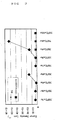
- the result after the second pattern of heat treatment was performed on the carbon doped wafer is shown in Fig. 3.
- the isothermal heat treatment at 700°C for 1 to 8 hours or at 750°C for 2 to 16 hours is the heat treatment for forming the oxygen precipitate nucleus, and also the heat treatment for generating a new donor.
- the OD treatment at 1150°C for 3.5 hours is performed, the oxygen donor is prevented from being generated after the isothermal heat treatment.
- the oxygen donor is more prevented from being generated until the heat treatment at 400°C for 2 hours by the OD treatment at 1150°C for 3.5 hours or the subsequent heat treatment for generating the oxygen precipitate nucleus at 750°C.
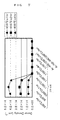
- the high-temperature heat treatment at 1000°C for 16 hours as the heat treatment for growing the oxygen precipitate is more effective in preventing the oxygen donor generation and its effectiveness is not influenced by the remaining oxygen concentration.
- the result when the third heat treatment was performed on the carbon non-doped wafer is shown in Fig. 5(a) and 5(b).
- Fig. 5(a) when the OD treatment is performed, the remaining oxygen concentration is not sufficiently lowered even if the treatment time at the isothermal heat treatment is increased, and it is difficult to prevent the oxygen thermal donor from being generated.
- Fig. 5(b) when the OD treatment is not performed, the remaining oxygen concentration is lowered (the oxygen precipitate is increased) as the treatment time in the isothermal heat treatment is increased and accordingly the oxygen donor is prevented from being generated, but its effect is not so much as the effect provided by the carbon doping shown in Fig. 4(c).
- the DZ layer is not provided by the heat treatment without the OD treatment, it cannot be applied to the device.
- the OD treatment was performed on the carbon non-doped wafer having an initial oxygen concentration of 15 ⁇ 10 17 atoms/cm 3 and the heat treatments at 700°C for 64 hours and at 1000°C for 16 hours were performed.
- the remaining oxygen concentration is only lowered to 12 ⁇ 10 17 atoms/cm 3 and the oxygen thermal donor is not sufficiently prevented from being generated, so that a further long time unrealistic heat treatment is needed.
- a sintering heat treatment is performed at 400°C or 350°C for about 30 minutes after a wiring process of metal such as Al or Cu.
- This metal wiring is laminated to be several layers and the above described heat treatment is performed on each layer. Therefore, even when the heat treatment at 400°C for about 2 hours is performed, it is necessary to maintain resistivity which is 100 ⁇ cm or more and preferably 1000 ⁇ cm or more. Since there is a measurement error in the 4-probe measurement, in the case of the p type after the DK treatment, a value lower than the resistance value is provided in some cases. Its variation is within 5 ⁇ 10 12 atoms/cm 3 in terms of a donor amount.
- the following 5 kinds of 8-inch sample wafers were cut out from a silicon single crystal grown by the CZ method.
- the first sample wafer is a P type carbon non-doped product in which resistivity is 1000 ⁇ cm and an oxygen concentration is 15 ⁇ 10 17 atoms/cm 3 .
- the second to fifth sample wafers are P type carbon doped products in which resistivity is 1000 ⁇ cm, an oxygen concentration is 15 ⁇ 10 17 atoms/cm 3 , and a carbon concentration is 5 ⁇ 10 15 , 1 ⁇ 10 16 , 5 ⁇ 10 16 , 1 ⁇ 10 17 atoms/cm 3 .
- a heat treatment for eliminating the oxygen donor was performed on each of the above wafers at 650°C for 30 minutes and then the OD treatment was performed at 1150°C for 3.5 hours in a nitrogen atmosphere containing 3% of oxygen. Then, an isothermal heat treatment was performed in a nitrogen atmosphere containing 3% of oxygen as a heat treatment for forming oxygen precipitate nucleus at 700°C for 8 hours on the carbon non-doped wafer and at 750°C for 2 hours on the carbon doped wafer, and then, a high-temperature heat treatment was performed on these wafers in the nitrogen atmosphere as a heat treatment for growing the oxygen precipitate at 1000°C for 16 hours.
- a heat treatment for generating the oxygen thermal donor was performed at 400°C for 4 hours in the nitrogen atmosphere on each of the DZ-IG processed wafer.
- An amount of oxygen donors was calculated from the result from measurement of resistivity of each wafer after the heat treatment.
- variation in resistivity is small and the amount of oxygen donors is within an allowable range, meanwhile in the case of the carbon non-doped wafer, the oxygen donors are generated beyond the allowable value.
- the oxygen donor is effectively prevented from being generated when the carbon concentration.is 5 ⁇ 10 15 atoms/cm 3 or more.
- the following 2 kinds of 8-inch sample wafers were cut out from a silicon single crystal grown by the CZ method.
- the first sample wafer is a P type carbon non-doped product in which resistivity is 1000 ⁇ cm and an oxygen concentration is 15 ⁇ 10 17 atoms/cm 3 .
- the second sample wafer is a P type carbon doped product in which resistivity is 1000 ⁇ cm, an oxygen concentration is 15 ⁇ 10 17 atoms/cm 3 , and carbon concentration is 1 ⁇ 10 16 atoms/cm 3 .
- the carbon doped wafer was annealed with hydrogen at 800 to 1150°C for 1 to 4 hours. Then, a heat treatment was performed at 1200°C for 1 hour in an atmosphere of argon gas and an atmosphere of mixture gas of argon gas and hydrogen gas besides in the hydrogen gas atmosphere.
- the used wafers were both the second sample wafers.
- the heat treatment for generating the oxygen donor was performed on each wafer in the nitrogen atmosphere at 450°C in which the oxygen donor is likely to be generated more than at 400°C, changing the time for 1 hour, 2 hours and 4 hours.
- the resistivity of each wafer after the heat treatment was measured and an amount of oxygen donor generated was found from the above result. The oxygen donor amount is shown in Fig. 7.
- the oxygen donor was generated beyond the allowable value until the heat treatment at 1000°C for 1 hour, the amount of oxygen donor generated was not more than the allowable value at 1100°C or more for 1 hour or more.
- the heat treatment was performed at 1200°C for 1 hour in the argon gas atmosphere and in the atmosphere of the mixture gas of argon gas and hydrogen gas, the amount of oxygen donor generated is not more than the allowable value. That is, it is found that the oxygen donor can be effectively prevented from being generated when the heat treatment is performed at 1100°C or more for 1 hour or more in a non-oxidizing gas atmosphere.
- a 8-inch wafer was cut out from a silicon single crystal grown by the CZ method.
- the wafer is a P type wafer in which resistivity is 2000 ⁇ cm, an oxygen concentration is 15 ⁇ 10 17 atoms/cm 3 , and a carbon concentration is 1 ⁇ 10 16 atoms/cm 3 .
- the heat treatment for eliminating the oxygen donor was performed on the wafer at 650°C for 30 minutes and then the following heat treatment was performed.
- the OD treatment was performed at 1150°C for 3.5 hours in the nitrogen atmosphere containing 3% of oxygen, and then the heat treatment for forming the oxygen precipitate nucleus was performed at 750°C for 2 hours in the similar atmosphere.
- epitaxial growing treatment was performed on the wafer so as to provide a P type layer having resistivity 10 ⁇ cm and a thickness 5 ⁇ m.
- the resistivity of the substrate is maintained at 2000 ⁇ cm or more which is the same as that after the DK treatment.
- the following 2 kinds of 8-inch sample wafers were cut out from a silicon single crystal grown by the CZ method.
- the first sample wafer is a P type carbon non-doped product in which resistivity is 1000 ⁇ cm and an oxygen concentration is 15 ⁇ 10 17 atoms/cm 3 .
- the second sample wafer is a P type carbon doped product in which resistivity is 1000 ⁇ cm, an oxygen concentration is 15 ⁇ 10 17 atoms/cm 3 , and a carbon concentration is 1 ⁇ 10 16 atoms/cm 3 .
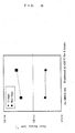
- the heat treatment for generating the thermal donor was performed at 400°C for 4 hours in the nitrogen atmosphere on the SIMOX wafers which was manufactured from the carbon doped wafer and the carbon non-doped wafer.
- the result from the measurement of the oxygen donor density after the heat treatment for generating the thermal donor is shown in Fig. 8.
- the oxygen donor is prevented from being generated in the carbon-doped SIMOX wafer. Meanwhile, although the generation of the oxygen donor is prevented a little in the carbon non-doped SIMOX wafer, its effect is not so much as the effect in the carbon-doped SIMOX wafer.
- the following 2 kinds of 8-inch sample wafers were cut out from a silicon single crystal grown by the CZ method.
- the first sample wafer is a P type carbon non-doped product in which resistivity is 1000 ⁇ cm and an oxygen concentration is 15 ⁇ 10 17 atoms/cm 3 .
- the second sample wafer is a P type carbon doped product in which resistivity is 1000 ⁇ cm, an oxygen concentration is 15 ⁇ 10 17 atoms/cm 3 , and a carbon concentration is 1 ⁇ 10 16 atoms/cm 3 .
- the heat treatment for generating the thermal donor was performed at 400°C for 4 hours in the nitrogen atmosphere on the bonded SOI wafers which were manufactured with the carbon doped wafer and the carbon non-doped wafer.
- An oxygen donor density was measured after the heat treatment for generating the thermal donor. Resistivity of the bonded carbon-doped wafer was small in variation from the resistivity after the DK treatment and generation of the oxygen donor was prevented within an allowable range. Meanwhile, according to the bonded carbon non-doped wafer, although the generation of the oxygen donor was prevented a little, its effect was not so much as that in the bonded carbon doped wafer.
- the high-resistance silicon wafer of the present invention generation of the oxygen donor can be prevented in the heat treatment for forming circuits which is to be performed on the side of the device manufacturer by carbon doping without lowering a remaining oxygen concentration.
- the mechanical strength of the wafer can be maintained and heat treatment costs can be lowered.
- an appropriate amount of oxygen precipitate is generated without being influenced by the remaining oxygen concentration, an excellent gettering ability can be provided.
- the generation of the oxygen donor can be effectively prevented by performing the heat treatment which is effective in preventing the generation of the oxygen donor in addition to the carbon doping. Furthermore, since various kinds of heat treatments which are peculiar to a wafer type can be used as the above heat treatment, an increase in heat treatment costs can be avoided and excellent economical efficiency is provided.
Landscapes
- Chemical & Material Sciences (AREA)
- Engineering & Computer Science (AREA)
- Crystallography & Structural Chemistry (AREA)
- Materials Engineering (AREA)
- Metallurgy (AREA)
- Organic Chemistry (AREA)
- Crystals, And After-Treatments Of Crystals (AREA)
Abstract
Description
Claims (17)
- A high-resistance silicon wafer having resistivity of 100 Ωcm or more, wherein a carbon concentration is 5 × 10¹⁵ to 5 × 10¹⁷ atoms/cm3.
- The high-resistance silicon wafer according to claim 1, wherein an oxygen concentration in the wafer is beyond 8 × 10¹⁷ atoms/cm3 (Old-ASTM).
- The high-resistance silicon wafer according to claim 1 or 2, wherein a DZ (Denuded Zone) layer is formed at least 5 µm or more in depth from a surface of the wafer.
- The high-resistance silicon wafer according to any one of claims 1 to 3, wherein a density of a LPD (Light Point Defect) having a size of 0.12 µm or more and observed on a surface of the wafer is controlled so as to be 0.2/cm2 or less.
- An epitaxial wafer having a high-resistance silicon wafer according to any one of claims 1 to 4 as a base wafer.
- An SOI wafer having a high-resistance silicon wafer according to any one of claims 1 to 5 as a base wafer.
- The SOI wafer according to claim 6, which is a bonded wafer or a SIMOX wafer.
- A method of manufacturing a high-resistance silicon wafer, characterized in that a heat treatment which is effective in preventing an oxygen donor from being generated is performed on a silicon wafer having a resistivity of 100 Ωcm or more and a carbon concentration of 5 × 10¹⁵ to 5 × 10¹⁷ atoms/cm3.
- The method of manufacturing a high-resistance silicon wafer according to claim 8, wherein a remaining oxygen concentration after the heat treatment is 6.5 × 10¹⁷ atoms/cm3 (Old-ASTM) or more.
- The method of manufacturing a high-resistance silicon wafer according to claim 8, wherein the heat treatment is a high-temperature heat treatment at 1100°C or higher.
- The method of manufacturing a high-resistance silicon wafer according to claim 8, wherein the heat treatment is an oxygen out-diffusion treatment for forming a DZ (Denuated Zone) layer on a wafer surface.
- The method of manufacturing a high-resistance silicon wafer according to claim 11, characterized in that after the oxygen out-diffusion treatment, a heat treatment for forming an oxygen precipitate nucleus, or the heat treatment for forming the oxygen precipitate nucleus and a heat treatment for growing an oxygen precipitate are performed.
- The method of manufacturing a high-resistance silicon wafer according to claim 8, wherein the heat treatment is high-temperature annealing treatment for eliminating a COP which is a void defect caused by a hole from a wafer surface.
- A method of manufacturing an SOI wafer, characterized by manufacturing an SIMOX type of SOI wafer comprising a high-resistance silicon wafer having resistivity of 100 Ωcm or more and a carbon concentration of 5 × 10¹⁵ to 5 × 10¹⁷ atoms/cm3 as a base wafer.
- The method of manufacturing an SOI wafer according to claim 14, wherein a high-temperature heat treatment for forming a BOX layer in a SIMOX type of SOI wafer manufacturing process serves also as a heat treatment which is effective in preventing generation of an oxygen donor.
- A method of manufacturing an SOI wafer, characterized by manufacturing a bonded type of SOI wafer comprising a high-resistance silicon wafer having resistivity of 100 Ωcm or more and a carbon concentration of 5 × 10¹⁵ to 5 × 10¹⁷ atoms/cm3 as a base wafer.
- The method of manufacturing the SOI wafer according to claim 16, wherein the high-temperature heat treatment performed in the bonded type of SOI wafer manufacturing process serves also as a heat treatment which is effective in preventing the generation of the oxygen donor.
Applications Claiming Priority (3)
| Application Number | Priority Date | Filing Date | Title |
|---|---|---|---|
| JP2002208515 | 2002-07-17 | ||
| JP2002208515 | 2002-07-17 | ||
| PCT/JP2003/008333 WO2004008521A1 (en) | 2002-07-17 | 2003-06-30 | High-resistance silicon wafer and process for producing the same |
Publications (3)
| Publication Number | Publication Date |
|---|---|
| EP1542269A1 true EP1542269A1 (en) | 2005-06-15 |
| EP1542269A4 EP1542269A4 (en) | 2008-03-05 |
| EP1542269B1 EP1542269B1 (en) | 2016-10-05 |
Family
ID=30112847
Family Applications (1)
| Application Number | Title | Priority Date | Filing Date |
|---|---|---|---|
| EP03741140.2A Expired - Lifetime EP1542269B1 (en) | 2002-07-17 | 2003-06-30 | A method of manufacturing a high-resistance silicon wafer |
Country Status (6)
| Country | Link |
|---|---|
| US (1) | US7316745B2 (en) |
| EP (1) | EP1542269B1 (en) |
| JP (1) | JP4970724B2 (en) |
| KR (1) | KR100685161B1 (en) |
| TW (1) | TWI246543B (en) |
| WO (1) | WO2004008521A1 (en) |
Cited By (3)
| Publication number | Priority date | Publication date | Assignee | Title |
|---|---|---|---|---|
| EP1895027A4 (en) * | 2005-06-20 | 2009-06-24 | Sumco Corp | PROCESS FOR PUSHING SINGLE SILICON CRYSTAL AND PROCESS FOR PRODUCING SILICON WAFER |
| EP2098620A1 (en) * | 2008-03-05 | 2009-09-09 | Sumco Corporation | Method of manufacturing silicon substrate |
| US7819972B2 (en) | 2005-06-20 | 2010-10-26 | Sumco Corporation | Method for growing silicon single crystal and method for manufacturing silicon wafer |
Families Citing this family (38)
| Publication number | Priority date | Publication date | Assignee | Title |
|---|---|---|---|---|
| CN100461349C (en) * | 2003-10-21 | 2009-02-11 | 株式会社上睦可 | Method for producing high-resistance silicon wafer, epitaxial wafer, and method for producing SOI wafer |
| JP2006073580A (en) * | 2004-08-31 | 2006-03-16 | Sumco Corp | Silicon epitaxial wafer and manufacturing method thereof |
| KR100749935B1 (en) | 2004-11-16 | 2007-08-16 | 주식회사 실트론 | Silicon Monocrystalline and Silicon Wafers |
| JP2006261632A (en) * | 2005-02-18 | 2006-09-28 | Sumco Corp | Heat treatment method for silicon wafer |
| JP5188673B2 (en) * | 2005-06-09 | 2013-04-24 | 株式会社Sumco | Silicon wafer for IGBT and method for manufacturing the same |
| JP2007045662A (en) * | 2005-08-10 | 2007-02-22 | Sumco Corp | Semiconductor silicon wafer and method for manufacturing the same |
| JP5103745B2 (en) * | 2006-01-31 | 2012-12-19 | 株式会社Sumco | High frequency diode and manufacturing method thereof |
| JP5076326B2 (en) * | 2006-01-31 | 2012-11-21 | 株式会社Sumco | Silicon wafer and manufacturing method thereof |
| JP4760729B2 (en) * | 2006-02-21 | 2011-08-31 | 株式会社Sumco | Silicon single crystal wafer for IGBT and manufacturing method of silicon single crystal wafer for IGBT |
| CN101351890A (en) * | 2006-09-07 | 2009-01-21 | 胜高股份有限公司 | Semiconductor substrate of solid-state image sensing device, solid-state image sensing device, and manufacturing method thereof |
| TW200818327A (en) * | 2006-09-29 | 2008-04-16 | Sumco Techxiv Corp | Silicon wafer heat treatment method |
| ATE493755T1 (en) * | 2007-05-02 | 2011-01-15 | Siltronic Ag | SILICON WAFER AND PRODUCTION PROCESS THEREOF |
| JP5239265B2 (en) * | 2007-09-07 | 2013-07-17 | 株式会社Sumco | Seed crystal for pulling silicon single crystal and method for producing silicon single crystal using the seed crystal |
| JP2009283533A (en) * | 2008-05-20 | 2009-12-03 | Sumco Corp | Wafer for back-illuminated solid-state image sensor, method of manufacturing the same, and back-illuminated solid-state image sensor |
| JP2010027959A (en) * | 2008-07-23 | 2010-02-04 | Sumco Corp | Method for manufacturing high-resistance simox wafer |
| JP5696349B2 (en) * | 2008-09-05 | 2015-04-08 | 株式会社Sumco | Manufacturing method of wafer for back irradiation type solid-state imaging device |
| EP2412849B1 (en) * | 2009-03-25 | 2016-03-23 | SUMCO Corporation | Silicon wafer and method for manufacturing same |
| JP5407473B2 (en) | 2009-03-25 | 2014-02-05 | 株式会社Sumco | Silicon wafer manufacturing method |
| FR2953640B1 (en) * | 2009-12-04 | 2012-02-10 | S O I Tec Silicon On Insulator Tech | METHOD FOR MANUFACTURING A SEMICONDUCTOR TYPE STRUCTURE ON INSULATION, WITH REDUCED ELECTRICAL LOSSES AND CORRESPONDING STRUCTURE |
| JP5544859B2 (en) * | 2009-12-15 | 2014-07-09 | 信越半導体株式会社 | Manufacturing method of silicon epitaxial wafer |
| JP2011138955A (en) * | 2009-12-28 | 2011-07-14 | Siltronic Japan Corp | Silicon wafer and manufacturing method therefor |
| CN103545169A (en) * | 2012-07-11 | 2014-01-29 | 上海华虹Nec电子有限公司 | Method for preventing wafer from buckling deformation |
| WO2014041736A1 (en) * | 2012-09-13 | 2014-03-20 | パナソニック株式会社 | Nitride semiconductor structure |
| JP5630527B2 (en) * | 2013-04-12 | 2014-11-26 | 株式会社Sumco | Manufacturing method of bonded SOI wafer |
| US8923439B1 (en) * | 2013-06-07 | 2014-12-30 | Intel IP Corporation | Complementary signal mixing |
| JP2015140270A (en) * | 2014-01-28 | 2015-08-03 | グローバルウェーハズ・ジャパン株式会社 | silicon wafer |
| US20150294868A1 (en) * | 2014-04-15 | 2015-10-15 | Infineon Technologies Ag | Method of Manufacturing Semiconductor Devices Containing Chalcogen Atoms |
| JP2015008314A (en) * | 2014-08-14 | 2015-01-15 | 株式会社Sumco | Method of producing epitaxial wafer and epitaxial wafer |
| FR3051968B1 (en) * | 2016-05-25 | 2018-06-01 | Soitec | METHOD FOR MANUFACTURING HIGH RESISTIVITY SEMICONDUCTOR SUBSTRATE |
| JP6669133B2 (en) * | 2017-06-23 | 2020-03-18 | 株式会社Sumco | Method for predicting thermal donor generation behavior of silicon wafer, method for evaluating silicon wafer, and method for manufacturing silicon wafer |
| JP6878188B2 (en) | 2017-07-26 | 2021-05-26 | グローバルウェーハズ・ジャパン株式会社 | How to measure the resistivity of a silicon wafer |
| JP6988737B2 (en) * | 2018-08-21 | 2022-01-05 | 株式会社Sumco | Manufacturing method of silicon wafer and silicon wafer |
| JP7090295B2 (en) * | 2020-06-24 | 2022-06-24 | グローバルウェーハズ・ジャパン株式会社 | Silicon wafers and methods for manufacturing silicon wafers |
| FR3112239B1 (en) * | 2020-07-03 | 2022-06-24 | Soitec Silicon On Insulator | SUPPORTING SUBSTRATE FOR SELF STRUCTURE AND ASSOCIATED METHOD OF MANUFACTURING |
| TWI865954B (en) * | 2021-11-04 | 2024-12-11 | 日商Sumco股份有限公司 | Silicon wafer and epitaxial silicon wafer |
| JP7658332B2 (en) | 2021-11-04 | 2025-04-08 | 株式会社Sumco | Silicon wafers and epitaxial silicon wafers |
| TWI854344B (en) * | 2021-11-04 | 2024-09-01 | 日商Sumco股份有限公司 | Silicon wafer and epitaxial silicon wafer |
| JP7616088B2 (en) | 2022-01-05 | 2025-01-17 | 信越半導体株式会社 | Nitride semiconductor substrate and method for producing same |
Family Cites Families (15)
| Publication number | Priority date | Publication date | Assignee | Title |
|---|---|---|---|---|
| JP2770091B2 (en) * | 1991-11-22 | 1998-06-25 | コマツ電子金属株式会社 | Silicon wafer processing method |
| KR0139730B1 (en) * | 1993-02-23 | 1998-06-01 | 사또오 후미오 | Semiconductor substrate and manufacturing method thereof |
| JPH10150048A (en) * | 1996-11-15 | 1998-06-02 | Sumitomo Sitix Corp | Semiconductor substrate |
| JPH11312649A (en) * | 1998-04-30 | 1999-11-09 | Nippon Asm Kk | Cvd device |
| EP1087041B1 (en) | 1999-03-16 | 2009-01-07 | Shin-Etsu Handotai Co., Ltd | Production method for silicon wafer and silicon wafer |
| JP2001217251A (en) * | 1999-11-26 | 2001-08-10 | Mitsubishi Materials Silicon Corp | Method of heat-treating silicon wafer |
| JP4605876B2 (en) * | 2000-09-20 | 2011-01-05 | 信越半導体株式会社 | Silicon wafer and silicon epitaxial wafer manufacturing method |
| US6673147B2 (en) * | 2001-12-06 | 2004-01-06 | Seh America, Inc. | High resistivity silicon wafer having electrically inactive dopant and method of producing same |
| EP1493179B1 (en) * | 2002-04-10 | 2007-12-12 | MEMC Electronic Materials, Inc. | Silicon wafer and process for controlling denuded zone depth in an ideal oxygen precipitating silicon wafer |
| JP2004006615A (en) * | 2002-04-26 | 2004-01-08 | Sumitomo Mitsubishi Silicon Corp | High resistance silicon wafer and method of manufacturing the same |
| US6905771B2 (en) * | 2002-11-11 | 2005-06-14 | Sumitomo Mitsubishi Silicon Corporation | Silicon wafer |
| CN100461349C (en) * | 2003-10-21 | 2009-02-11 | 株式会社上睦可 | Method for producing high-resistance silicon wafer, epitaxial wafer, and method for producing SOI wafer |
| JP5010091B2 (en) * | 2003-11-13 | 2012-08-29 | 株式会社Sumco | High resistance silicon wafer |
| JP4604889B2 (en) * | 2005-05-25 | 2011-01-05 | 株式会社Sumco | Silicon wafer manufacturing method and silicon single crystal growing method |
| US7485928B2 (en) * | 2005-11-09 | 2009-02-03 | Memc Electronic Materials, Inc. | Arsenic and phosphorus doped silicon wafer substrates having intrinsic gettering |
-
2003
- 2003-06-30 EP EP03741140.2A patent/EP1542269B1/en not_active Expired - Lifetime
- 2003-06-30 US US10/519,837 patent/US7316745B2/en not_active Expired - Lifetime
- 2003-06-30 KR KR1020057000629A patent/KR100685161B1/en not_active Expired - Lifetime
- 2003-06-30 WO PCT/JP2003/008333 patent/WO2004008521A1/en not_active Ceased
- 2003-06-30 JP JP2004521140A patent/JP4970724B2/en not_active Expired - Lifetime
- 2003-07-16 TW TW092119396A patent/TWI246543B/en not_active IP Right Cessation
Cited By (3)
| Publication number | Priority date | Publication date | Assignee | Title |
|---|---|---|---|---|
| EP1895027A4 (en) * | 2005-06-20 | 2009-06-24 | Sumco Corp | PROCESS FOR PUSHING SINGLE SILICON CRYSTAL AND PROCESS FOR PRODUCING SILICON WAFER |
| US7819972B2 (en) | 2005-06-20 | 2010-10-26 | Sumco Corporation | Method for growing silicon single crystal and method for manufacturing silicon wafer |
| EP2098620A1 (en) * | 2008-03-05 | 2009-09-09 | Sumco Corporation | Method of manufacturing silicon substrate |
Also Published As
| Publication number | Publication date |
|---|---|
| TWI246543B (en) | 2006-01-01 |
| JP4970724B2 (en) | 2012-07-11 |
| WO2004008521A1 (en) | 2004-01-22 |
| KR20050035862A (en) | 2005-04-19 |
| US7316745B2 (en) | 2008-01-08 |
| JPWO2004008521A1 (en) | 2005-11-17 |
| US20050250349A1 (en) | 2005-11-10 |
| EP1542269B1 (en) | 2016-10-05 |
| EP1542269A4 (en) | 2008-03-05 |
| KR100685161B1 (en) | 2007-02-22 |
| TW200404924A (en) | 2004-04-01 |
Similar Documents
| Publication | Publication Date | Title |
|---|---|---|
| US7316745B2 (en) | High-resistance silicon wafer and process for producing the same | |
| US7397110B2 (en) | High resistance silicon wafer and its manufacturing method | |
| US7803228B2 (en) | Process for producing high-resistance silicon wafers and process for producing epitaxial wafers and SOI wafers | |
| KR100319413B1 (en) | Method for manufacturing semiconductor silicon epitaxial wafer and semiconductor device | |
| KR101020436B1 (en) | Silicon Single Crystal Wafer and Manufacturing Method Thereof | |
| EP1471578A1 (en) | Soi wafer manufacturing method and soi wafer | |
| JP2008294112A (en) | Silicon single crystal wafer and manufacturing method thereof | |
| JP4013276B2 (en) | Manufacturing method of silicon epitaxial wafer | |
| KR20090006878A (en) | Method for manufacturing SIO substrate and SIO substrate obtained by the method | |
| WO2002049091A1 (en) | Anneal wafer manufacturing method and anneal wafer | |
| JP5103745B2 (en) | High frequency diode and manufacturing method thereof | |
| JP2011054656A (en) | High resistivity silicon wafer and manufacturing method thereof | |
| KR100834231B1 (en) | Manufacturing Method of SIOMO Substrate | |
| JP2010062291A (en) | Semiconductor substrate and its manufacturing method | |
| JP2011054655A (en) | Silicon wafer for high-frequency device and manufacturing method thereof | |
| JP5922858B2 (en) | Manufacturing method of high resistance silicon wafer | |
| JP2005175390A (en) | Simox substrate and its manufacturing method | |
| JP5922860B2 (en) | Manufacturing method of high resistance silicon wafer | |
| JP2006332689A (en) | Method of manufacturing silicon epitaxial wafer | |
| JP2004087665A (en) | High resistor silicon wafer | |
| JP2003142668A (en) | Method and manufacturing simox substrate | |
| JP2020031105A (en) | Manufacturing method of silicon wafer and silicon wafer |
Legal Events
| Date | Code | Title | Description |
|---|---|---|---|
| PUAI | Public reference made under article 153(3) epc to a published international application that has entered the european phase |
Free format text: ORIGINAL CODE: 0009012 |
|
| 17P | Request for examination filed |
Effective date: 20050105 |
|
| AK | Designated contracting states |
Kind code of ref document: A1 Designated state(s): AT BE BG CH CY CZ DE DK EE ES FI FR GB GR HU IE IT LI LU MC NL PT RO SE SI SK TR |
|
| RAP1 | Party data changed (applicant data changed or rights of an application transferred) |
Owner name: SUMCO CORPORATION |
|
| A4 | Supplementary search report drawn up and despatched |
Effective date: 20080131 |
|
| 17Q | First examination report despatched |
Effective date: 20110512 |
|
| REG | Reference to a national code |
Ref country code: DE Ref legal event code: R079 Ref document number: 60349461 Country of ref document: DE Free format text: PREVIOUS MAIN CLASS: H01L0021322000 Ipc: C30B0029060000 |
|
| GRAP | Despatch of communication of intention to grant a patent |
Free format text: ORIGINAL CODE: EPIDOSNIGR1 |
|
| RIC1 | Information provided on ipc code assigned before grant |
Ipc: H01L 21/322 20060101ALI20160503BHEP Ipc: H01L 21/762 20060101ALI20160503BHEP Ipc: H01L 27/12 20060101ALI20160503BHEP Ipc: C30B 29/06 20060101AFI20160503BHEP Ipc: C30B 33/00 20060101ALI20160503BHEP |
|
| INTG | Intention to grant announced |
Effective date: 20160520 |
|
| RIN1 | Information on inventor provided before grant (corrected) |
Inventor name: TAKAO, HIROYUKI, C/O SUMITOMO MITSUBISHI Inventor name: SADAMITSU, SHINSUKE, C/O SUMITOMO MITSUBISHI Inventor name: SUEOKA, KOUJI, C/O SUMITOMO MITSUBISHI Inventor name: HORAI, MASATAKA, C/O SUMITOMO MITSUBISHI Inventor name: TAKASE, NOBUMITSU, C/O SUMITOMO MITSUBISHI |
|
| GRAS | Grant fee paid |
Free format text: ORIGINAL CODE: EPIDOSNIGR3 |
|
| GRAA | (expected) grant |
Free format text: ORIGINAL CODE: 0009210 |
|
| AK | Designated contracting states |
Kind code of ref document: B1 Designated state(s): AT BE BG CH CY CZ DE DK EE ES FI FR GB GR HU IE IT LI LU MC NL PT RO SE SI SK TR |
|
| REG | Reference to a national code |
Ref country code: GB Ref legal event code: FG4D |
|
| REG | Reference to a national code |
Ref country code: CH Ref legal event code: EP |
|
| REG | Reference to a national code |
Ref country code: AT Ref legal event code: REF Ref document number: 834772 Country of ref document: AT Kind code of ref document: T Effective date: 20161015 |
|
| REG | Reference to a national code |
Ref country code: IE Ref legal event code: FG4D |
|
| REG | Reference to a national code |
Ref country code: DE Ref legal event code: R096 Ref document number: 60349461 Country of ref document: DE |
|
| REG | Reference to a national code |
Ref country code: NL Ref legal event code: MP Effective date: 20161005 |
|
| REG | Reference to a national code |
Ref country code: AT Ref legal event code: MK05 Ref document number: 834772 Country of ref document: AT Kind code of ref document: T Effective date: 20161005 |
|
| PG25 | Lapsed in a contracting state [announced via postgrant information from national office to epo] |
Ref country code: GR Free format text: LAPSE BECAUSE OF FAILURE TO SUBMIT A TRANSLATION OF THE DESCRIPTION OR TO PAY THE FEE WITHIN THE PRESCRIBED TIME-LIMIT Effective date: 20170106 Ref country code: SE Free format text: LAPSE BECAUSE OF FAILURE TO SUBMIT A TRANSLATION OF THE DESCRIPTION OR TO PAY THE FEE WITHIN THE PRESCRIBED TIME-LIMIT Effective date: 20161005 |
|
| PG25 | Lapsed in a contracting state [announced via postgrant information from national office to epo] |
Ref country code: FI Free format text: LAPSE BECAUSE OF FAILURE TO SUBMIT A TRANSLATION OF THE DESCRIPTION OR TO PAY THE FEE WITHIN THE PRESCRIBED TIME-LIMIT Effective date: 20161005 Ref country code: NL Free format text: LAPSE BECAUSE OF FAILURE TO SUBMIT A TRANSLATION OF THE DESCRIPTION OR TO PAY THE FEE WITHIN THE PRESCRIBED TIME-LIMIT Effective date: 20161005 Ref country code: PT Free format text: LAPSE BECAUSE OF FAILURE TO SUBMIT A TRANSLATION OF THE DESCRIPTION OR TO PAY THE FEE WITHIN THE PRESCRIBED TIME-LIMIT Effective date: 20170206 Ref country code: AT Free format text: LAPSE BECAUSE OF FAILURE TO SUBMIT A TRANSLATION OF THE DESCRIPTION OR TO PAY THE FEE WITHIN THE PRESCRIBED TIME-LIMIT Effective date: 20161005 Ref country code: ES Free format text: LAPSE BECAUSE OF FAILURE TO SUBMIT A TRANSLATION OF THE DESCRIPTION OR TO PAY THE FEE WITHIN THE PRESCRIBED TIME-LIMIT Effective date: 20161005 Ref country code: BE Free format text: LAPSE BECAUSE OF FAILURE TO SUBMIT A TRANSLATION OF THE DESCRIPTION OR TO PAY THE FEE WITHIN THE PRESCRIBED TIME-LIMIT Effective date: 20161005 |
|
| REG | Reference to a national code |
Ref country code: DE Ref legal event code: R097 Ref document number: 60349461 Country of ref document: DE |
|
| PG25 | Lapsed in a contracting state [announced via postgrant information from national office to epo] |
Ref country code: EE Free format text: LAPSE BECAUSE OF FAILURE TO SUBMIT A TRANSLATION OF THE DESCRIPTION OR TO PAY THE FEE WITHIN THE PRESCRIBED TIME-LIMIT Effective date: 20161005 Ref country code: DK Free format text: LAPSE BECAUSE OF FAILURE TO SUBMIT A TRANSLATION OF THE DESCRIPTION OR TO PAY THE FEE WITHIN THE PRESCRIBED TIME-LIMIT Effective date: 20161005 Ref country code: CZ Free format text: LAPSE BECAUSE OF FAILURE TO SUBMIT A TRANSLATION OF THE DESCRIPTION OR TO PAY THE FEE WITHIN THE PRESCRIBED TIME-LIMIT Effective date: 20161005 Ref country code: SK Free format text: LAPSE BECAUSE OF FAILURE TO SUBMIT A TRANSLATION OF THE DESCRIPTION OR TO PAY THE FEE WITHIN THE PRESCRIBED TIME-LIMIT Effective date: 20161005 Ref country code: RO Free format text: LAPSE BECAUSE OF FAILURE TO SUBMIT A TRANSLATION OF THE DESCRIPTION OR TO PAY THE FEE WITHIN THE PRESCRIBED TIME-LIMIT Effective date: 20161005 |
|
| PLBE | No opposition filed within time limit |
Free format text: ORIGINAL CODE: 0009261 |
|
| STAA | Information on the status of an ep patent application or granted ep patent |
Free format text: STATUS: NO OPPOSITION FILED WITHIN TIME LIMIT |
|
| PG25 | Lapsed in a contracting state [announced via postgrant information from national office to epo] |
Ref country code: BG Free format text: LAPSE BECAUSE OF FAILURE TO SUBMIT A TRANSLATION OF THE DESCRIPTION OR TO PAY THE FEE WITHIN THE PRESCRIBED TIME-LIMIT Effective date: 20170105 Ref country code: IT Free format text: LAPSE BECAUSE OF FAILURE TO SUBMIT A TRANSLATION OF THE DESCRIPTION OR TO PAY THE FEE WITHIN THE PRESCRIBED TIME-LIMIT Effective date: 20161005 |
|
| 26N | No opposition filed |
Effective date: 20170706 |
|
| PG25 | Lapsed in a contracting state [announced via postgrant information from national office to epo] |
Ref country code: SI Free format text: LAPSE BECAUSE OF FAILURE TO SUBMIT A TRANSLATION OF THE DESCRIPTION OR TO PAY THE FEE WITHIN THE PRESCRIBED TIME-LIMIT Effective date: 20161005 |
|
| PG25 | Lapsed in a contracting state [announced via postgrant information from national office to epo] |
Ref country code: MC Free format text: LAPSE BECAUSE OF FAILURE TO SUBMIT A TRANSLATION OF THE DESCRIPTION OR TO PAY THE FEE WITHIN THE PRESCRIBED TIME-LIMIT Effective date: 20161005 |
|
| REG | Reference to a national code |
Ref country code: CH Ref legal event code: PL |
|
| GBPC | Gb: european patent ceased through non-payment of renewal fee |
Effective date: 20170630 |
|
| REG | Reference to a national code |
Ref country code: FR Ref legal event code: ST Effective date: 20180228 |
|
| REG | Reference to a national code |
Ref country code: IE Ref legal event code: MM4A |
|
| PG25 | Lapsed in a contracting state [announced via postgrant information from national office to epo] |
Ref country code: LU Free format text: LAPSE BECAUSE OF NON-PAYMENT OF DUE FEES Effective date: 20170630 Ref country code: IE Free format text: LAPSE BECAUSE OF NON-PAYMENT OF DUE FEES Effective date: 20170630 Ref country code: CH Free format text: LAPSE BECAUSE OF NON-PAYMENT OF DUE FEES Effective date: 20170630 Ref country code: LI Free format text: LAPSE BECAUSE OF NON-PAYMENT OF DUE FEES Effective date: 20170630 Ref country code: GB Free format text: LAPSE BECAUSE OF NON-PAYMENT OF DUE FEES Effective date: 20170630 |
|
| PG25 | Lapsed in a contracting state [announced via postgrant information from national office to epo] |
Ref country code: FR Free format text: LAPSE BECAUSE OF NON-PAYMENT OF DUE FEES Effective date: 20170630 |
|
| PG25 | Lapsed in a contracting state [announced via postgrant information from national office to epo] |
Ref country code: HU Free format text: LAPSE BECAUSE OF FAILURE TO SUBMIT A TRANSLATION OF THE DESCRIPTION OR TO PAY THE FEE WITHIN THE PRESCRIBED TIME-LIMIT; INVALID AB INITIO Effective date: 20030630 |
|
| PG25 | Lapsed in a contracting state [announced via postgrant information from national office to epo] |
Ref country code: CY Free format text: LAPSE BECAUSE OF NON-PAYMENT OF DUE FEES Effective date: 20161005 |
|
| PG25 | Lapsed in a contracting state [announced via postgrant information from national office to epo] |
Ref country code: TR Free format text: LAPSE BECAUSE OF FAILURE TO SUBMIT A TRANSLATION OF THE DESCRIPTION OR TO PAY THE FEE WITHIN THE PRESCRIBED TIME-LIMIT Effective date: 20161005 |
|
| PGFP | Annual fee paid to national office [announced via postgrant information from national office to epo] |
Ref country code: DE Payment date: 20220620 Year of fee payment: 20 |
|
| REG | Reference to a national code |
Ref country code: DE Ref legal event code: R071 Ref document number: 60349461 Country of ref document: DE |