EP1540844B1 - Verfahren zum senden einer signalform mit steuerbarer dämpfung und ausbreitungsgeschwindigkeit - Google Patents
Verfahren zum senden einer signalform mit steuerbarer dämpfung und ausbreitungsgeschwindigkeit Download PDFInfo
- Publication number
- EP1540844B1 EP1540844B1 EP03793136.7A EP03793136A EP1540844B1 EP 1540844 B1 EP1540844 B1 EP 1540844B1 EP 03793136 A EP03793136 A EP 03793136A EP 1540844 B1 EP1540844 B1 EP 1540844B1
- Authority
- EP
- European Patent Office
- Prior art keywords
- time
- transmission medium
- waveform
- computing
- pulse
- Prior art date
- Legal status (The legal status is an assumption and is not a legal conclusion. Google has not performed a legal analysis and makes no representation as to the accuracy of the status listed.)
- Expired - Lifetime
Links
Images


Classifications
-
- H—ELECTRICITY
- H04—ELECTRIC COMMUNICATION TECHNIQUE
- H04L—TRANSMISSION OF DIGITAL INFORMATION, e.g. TELEGRAPHIC COMMUNICATION
- H04L25/00—Baseband systems
- H04L25/02—Details ; arrangements for supplying electrical power along data transmission lines
- H04L25/12—Compensating for variations in line impedance
-
- G—PHYSICS
- G01—MEASURING; TESTING
- G01R—MEASURING ELECTRIC VARIABLES; MEASURING MAGNETIC VARIABLES
- G01R31/00—Arrangements for testing electric properties; Arrangements for locating electric faults; Arrangements for electrical testing characterised by what is being tested not provided for elsewhere
- G01R31/08—Locating faults in cables, transmission lines, or networks
- G01R31/088—Aspects of digital computing
-
- H—ELECTRICITY
- H04—ELECTRIC COMMUNICATION TECHNIQUE
- H04B—TRANSMISSION
- H04B3/00—Line transmission systems
- H04B3/02—Details
- H04B3/46—Monitoring; Testing
- H04B3/462—Testing group delay or phase shift, e.g. timing jitter
-
- H—ELECTRICITY
- H04—ELECTRIC COMMUNICATION TECHNIQUE
- H04B—TRANSMISSION
- H04B3/00—Line transmission systems
- H04B3/02—Details
- H04B3/46—Monitoring; Testing
- H04B3/462—Testing group delay or phase shift, e.g. timing jitter
- H04B3/466—Testing attenuation in combination with at least one of group delay and phase shift
-
- G—PHYSICS
- G01—MEASURING; TESTING
- G01R—MEASURING ELECTRIC VARIABLES; MEASURING MAGNETIC VARIABLES
- G01R31/00—Arrangements for testing electric properties; Arrangements for locating electric faults; Arrangements for electrical testing characterised by what is being tested not provided for elsewhere
- G01R31/08—Locating faults in cables, transmission lines, or networks
- G01R31/11—Locating faults in cables, transmission lines, or networks using pulse reflection methods
Definitions
- the invention relates generally to the field of signal transmission. More particularly, a representative embodiment of the invention relates to transmission line testing and communication.
- Transmission lines with their characteristic loss of signal as well as inherent time delay, may create problems in designing systems that employ a plurality of signals, which may be subject to delay and distortion.
- Typical signals used to generate inputs to transmission lines generally exhibit delay or propagation times that are not easily determinable. The propagation velocity of these waves is also variable with displacement along the transmission line.
- a Time Domain Reflectometer is a test instrument used to find faults in transmission lines and to empirically estimate transmission line lengths and other parameters characterizing the line, such as: inductance per unit length, capacitance per unit length, resistance per unit length and conductance per unit length.
- time-of-flight of a test pulse generated by the instrument and applied to the line.
- the time-of-flight may be measured by timing the passage of the pulse detected at two locations along the line.
- time-of-flight measurements can allow one to obtain the distance between measurement points or, in the case of a reflected wave, the distance from the pulse launch point to the location of the impedance change causing the pulse to be reflected and returned.
- TDR technology A fundamental limitation in TDR technology is the poor accuracy of TOF measurements in lossy, dispersive transmission lines.
- the relatively high TDR accuracy of TOF values obtainable in short low loss, low dispersion transmissions lines is possible only because the propagating test pulses keep their shape and amplitude in tact over the distances they travel during TOF measurements.
- dispersive, lossy long transmission lines the test pulses used in the art change shape, amplitude, and speed as they travel.
- An example can be found in WO167628 .
- an apparatus for determining an attenuation coefficient and a propagation velocity comprises: an exponential waveform generator; an input recorder coupled to an output of the exponential waveform generator; a transmission line under test coupled to the output of the exponential waveform generator; an output recorder coupled to the transmission line under test; an additional transmission line coupled to the transmission line under test; and a termination impedance coupled to the additional transmission line and to a ground.
- the context of the invention can include signal transmission.
- the context of the invention can include a method and/or apparatus for measuring and estimating transmission line parameters.
- the context of the invention can also include a method and/or apparatus for performing high-speed communication over a lossy, dispersive transmission line.
- a practical application of the invention that has value within the technological arts is in time domain reflectometry. Further, the invention is useful in conjunction with lossy transmission lines. The invention is also useful in conjunction with frequency dependent transmission lines. Another practical application of the invention that has value within the technological arts is high-speed communications. There are virtually imnumerable other uses for the invention. In fact, any application involving the transmission of a signal may benefit.
- a method for transmitting a waveform having a controllable attenuation and propagation velocity can be cost effective and advantageous.
- the invention improves quality and/or reduces costs compared to previous approaches.
- the invention includes a method and/or apparatus for utilizing a truncated waveform, coined a Speedy Delivery (SD) waveform by the inventors.
- SD Speedy Delivery
- An analysis of SD propagation in coupled lossy transmission lines is presented and practical considerations associated with truncating the SD waveforms are addressed.
- Parameters used to describe the propagation of the SD waveform are defined and techniques for determining their values are presented. These parameters include the Speedy Delivery propagation velocity, v SD , the Speedy Delivery attenuation coefficient, A SD , and the Speedy Delivery impedance, Z SD . These parameters may depend on properties of a transmission media as well as an exponential coefficient ⁇ (SD input signal parameter).
- the invention describes SD signal propagation in coupled transmission lines. An embodiment involving two transmission lines is illustrated. More complex configurations that include a larger number of coupled lines may be readily developed by one of ordinary skill in the art in light of this disclosure. Additionally, the behavior of the propagation of a slowly varying envelope of an optical pulse containing a truncated SD signal in a single mode communication fiber is described.
- the invention teaches a method for using SD test pulses to obtain empirical estimates of the SD signal propagation parameters, A SD and v SD , in lossy transmission lines, including those with frequency dependent parameters.
- the invention provides a method for utilizing a wideband, non-SD waveform in order to develop an empirical transfer function for a calibration length of a given transmission media.
- This transfer function may be used to simulate the transmission of SD waveforms with a wide range of values for the exponential coefficient ⁇ .
- the SD parameters A SD( ⁇ ) and v SD( ⁇ ) can be determined from these simulated waveforms.
- the inclusion of a simulation step in the calibration process can significantly reduce the experimental measurements needed to determine the values of A SD( ⁇ ) and v SD( ⁇ ) for a variety of values for ⁇ .
- the SD behavior of a media can then be determined by simulation, without the need for an SD waveform generator.
- the invention teaches a method for determining the SD impedance of a transmission line. It also illustrates the predicable variation of Z SD as a function of ⁇ . This predictability can allow a designer to control the transmission line SD impedance by appropriately selecting the parameter ⁇ .
- the invention also describes an alternate precision distance measurement method using truncated SD test pulses with high loss, long lines. As the test pulses travel down these lines, the attenuation can be so extensive that their amplitudes are too small for common threshold crossing time of flight measurements to be feasible.
- the invention includes a method for predicting an attenuation and overcoming this difficulty, extracting accurate length measurements for long lossy lines.
- the invention demonstrates the utility of the SD test waveform in accurately determining distances to impedance discontinuities. Examples show how to use SD wave propagation as the basis for an accurate time domain reflectometry (TDR) unit.
- This unit may include an SD waveform generator, a means of coupling with the transmission media, a means of measuring the applied and reflected waveforms, a display, memory storage, and computational ability to analyze and interpret the SD waveforms.
- the invention can also include a computer.
- the invention can include a method which can be applied to modify currently available TDR units to increase their accuracy. This modification may be a TDR software modification resulting in a nonrecurring unit manufacturing cost.
- a standard TDR waveform may be used to determine an empirical transfer function for the line under test, and this transfer function may then be used to simulate the propagation of the SD waveform. This process allows all the advantages of SD to be incorporated into currently available units with only a modification of existing computational algorithms, creating a virtual SD TDR unit.
- the truncated SD test pulse approach can also be applied to the propagation of acoustic waves in sonar and geophysical applications. Reflected acoustic signals can be used to accurately determine the location of underwater objects and to determine locations of geophysical strata boundaries. Empirical transfer functions can be determined and used to simulate SD pulse propagation eliminating the need to physically generate complex acoustic pulses.
- the invention provides an SD waveform that has several propagation properties in lossy, frequency dependent transmission media, which make it suitable for enhancing a data transmission scheme.
- the invention provides a method to increase the number of bits transmitted per pulse by varying the value of ⁇ to encode data on truncated SD waveforms.
- the example provided utilizes SD pulses with four different ⁇ 's sequentially transmitted on a 2kft cable. These SD pulses are received at the end of the cable with the exponential constants undistorted. The four pulses may be transmitted as positive or negative signals resulting in eight possible states. Therefore, each pulse represents three bits of transmitted information in each symbol period. This strategy can be used with short, low loss transmission lines.
- the invention also teaches the use of SD propagation properties to generate a set of pulses consisting of linear combinations of truncated SD waveforms that are orthogonal at the receiver. Data can be encoded on these pulses by varying their amplitude, and these amplitude-modulated pulses may be transmitted simultaneously on a transmission line. The individual pulse amplitudes are computed at the receiver taking advantage of their orthogonality. This method provides improved noise immunity, and can be used with longer, higher loss transmission lines.
- the invention also teaches the use of SD waveforms in digital circuits, specifically, on-chip clock circuits. It provides a method for utilizing truncated SD clock waveforms to reduce clock skew.
- V(x,t) De -A SD [x-v SD t]
- a SD is the exponential coefficient describing the attenuation of the SD signal as a function of distance along the line at a fixed time instant
- v SD is the SD signal propagation velocity.
- This analysis includes the net cross capacitance, C ij , and the net cross inductances, M i
- the SD solution is:
- V x t P ⁇ 1 ⁇ e ⁇ ⁇ ⁇ 1 ⁇ x ⁇ P ⁇ 1 ⁇ 1 ⁇ D 1 ⁇ e ⁇ 1 ⁇ t 0 + P ⁇ 2 ⁇ e ⁇ ⁇ ⁇ 2 ⁇ x ⁇ P ⁇ 1 ⁇ 2 ⁇ 0 D 2 ⁇ e ⁇ 2 ⁇ t , where P( ⁇ i ) is a real matrix.
- V 1 x t A 11 ⁇ e ⁇ ⁇ 1 ⁇ 1 ⁇ x e ⁇ 1 ⁇ t + A 21 ⁇ e ⁇ ⁇ 2 ⁇ 1 ⁇ x e ⁇ 1 ⁇ t + A 12 ⁇ e ⁇ ⁇ 1 ⁇ 2 ⁇ x e ⁇ 2 ⁇ t + A 22 ⁇ e ⁇ ⁇ 2 ⁇ 2 ⁇ x e ⁇ 2 ⁇ t
- a SD 11 ⁇ 1 ⁇ 1
- a SD 12 ⁇ 1 ⁇ 2
- a SD 21 ⁇ 2 ⁇ 1
- a SD 22 ⁇ 2 ⁇ 2
- v SD 11 ⁇ 1 ⁇ 1 ⁇ 1
- v SD 12 ⁇ 2 ⁇ 1 ⁇ 2
- v SD 21 ⁇ 1 ⁇ 2 ⁇ 1
- v SD 22 ⁇ 2 ⁇ 2 ⁇ 2 .
- Truncation may be accomplished by several methods, as is known in the art.
- the attenuation of the traveling SD wave may be viewed from the perspective of a moving reference frame traveling at the speed / LC 1 .
- V x ⁇ t ⁇ De ⁇ A SD ⁇ ⁇ x ⁇ ⁇ v SD ⁇ ⁇ t ⁇ + x ⁇ ⁇ LC
- V x ⁇ t ⁇ De ⁇ ⁇ t ⁇ e ⁇ A SD ⁇ ⁇ 1 ⁇ v SD ⁇ ⁇ LC ⁇ x ⁇ .
- V l , t ⁇ De ⁇ ⁇ t ⁇ e ⁇ A SD ⁇ ⁇ 1 ⁇ v SD ⁇ ⁇ LC ⁇ l .
- Coupled transmission lines can be treated in a similar fashion.
- V 1 l , t j V 1 0 t j A 11 ⁇ e ⁇ A SD 11 1 ⁇ v SD 11 L ⁇ C ⁇ l + A 21 ⁇ e ⁇ A SD 21 1 ⁇ v SD 21 L ⁇ C ⁇ l A 11 + A 21 + A 12 + A 22 ⁇ e ⁇ 2 ⁇ ⁇ 1 t i + A 12 ⁇ e ⁇ A SD 12 1 ⁇ v SD 12 L ⁇ C ⁇ l + A 22 ⁇ e ⁇ A SD 22 1 ⁇ v SD 22 L ⁇ C ⁇ l A 11 + A 21 ⁇ e ⁇ 1 ⁇ ⁇ 2 t i + A 12 + A 22 .
- Another example includes of the evolution of a slowly varying envelope, E(x, t), of an optical pulse in a single mode communication fiber.
- the Schrodinger partial differential equation [3], ⁇ E ⁇ x + ⁇ 1 ⁇ E ⁇ t ⁇ j 2 ⁇ 2 ⁇ 2 E ⁇ t ⁇ 1 6 ⁇ 3 ⁇ 3 E ⁇ t 3 ⁇ ⁇ 2 E , describes the evolution of the shape of the propagating pulse envelope undergoing chromatic dispersion in fiber.
- / ⁇ o ⁇ o is the phase velocity of the pulse.
- / ⁇ 1 1 is the group velocity
- ⁇ 2 is the group velocity dispersion (GVD) parameter which causes the pulse to broaden as it propagates in the fiber.
- ⁇ 3 is the third-order dispersion (TOD) parameter [4]
- the higher order derivatives of ⁇ with respect to ⁇ are assumed negligible. However, they may be added in these analyses by anyone familiar with the art.
- the fiber attenuation is represented by the parameter ⁇ .
- the receiver detector in a fiber optic communication network responds to the square of the magnitude
- the SD propagation speed in this moving reference frame is v ⁇ sd T o
- in x ⁇ , t ⁇ frame 1 T o ⁇ 2 ⁇ ⁇ 3 6 T o 3 ,
- This example teaches how SD test pulses may be used to obtain empirical estimates of the transmission line parameters, A SD and v SD , that describe the propagation of SD waveforms in lossy, dispersive lines, including those with frequency dependent parameters.
- the numerical values of A SD and v SD as a function of ⁇ can be determined empirically.
- FIG. 2 an experimental set up that may be used to determine these parameters for a copper, twisted wire pair transmission line is depicted.
- the test length of the transmission line, d, and the value of ⁇ for the applied SD input signal are measured.
- An additional length of transmission line that is identical to the line under test is attached as shown and terminated with an open circuit.
- the cables are two 24 AWG, individually shielded, twisted wire pairs in a 1002 ft coil of T1 cable.
- the values of D, ⁇ and the duration of the SD signal were chosen to prevent the occurrence of reflections at the measurement point, d, during the initial time of flight of the SD signal propagating in the test line.
- the additional length of transmission line also ensures that all reflections occurring in the test line are delayed until well after the propagating SD waveform measurement at d is complete.
- the SD signal time of flight can be directly measured by timing the propagating SD waveform crossing of constant voltage thresholds ( FIG. 3 ).
- the times of flight for these waveforms shown again in FIG. 4A at thresholds from 1.2 volts to 4.8 volts are plotted in FIG. 4B .
- the calculated A SD obtained from the waveforms shown in FIG.
- this type of threshold crossing TOF measurement can be used to determine the unknown length of another sample of the same transmission line.
- the average TOF for the threshold overlap region shown in FIG. 5B is 3,418 ns. This time of flight together with the previously calibrated v SD , results in an estimated distance of 1,996 ft, or 99.6% of the actual length (2004 ft).
- FIG. 5A also indicates a potential difficulty in longer lines caused by the attenuation of the truncated SD pulse.
- the region of SD threshold overlap grows smaller as the pulse propagates, and is attenuated over longer distances. The accuracy of this measurement can be improved, and the difficulty caused by the reduced region of threshold overlap can be overcome for very long transmission lines using the TOF measurement technique discussed in example 4.
- the high accuracy of this method results from the use of an average of TOF measurements taken over a range of signal threshold amplitudes. It is feasible to use the average of these values to improve the accuracy of the measurement of TOF since all points on the leading SD edge of the waveform travel at the same speed. This is in contrast with the current time domain reflectometry art in which a measurement of the time of emergence of the dispersing test pulse is attempted. This is equivalent to attempting to accurately measure the threshold crossing time of the pulse at a zero threshold level when the slope of the pulse is also nearly zero.
- the method described in example 1 can be limiting in that it should be experimentally repeated for each exponential coefficient ⁇ . This may require a lengthy laboratory calibration time for each cable type. Simulation can be included in the calibration process to significantly reduce the experimental measurements needed to determine the values of A SD and v SD .
- the use of simulation in this process requires a transfer function that describes the response of the specific type of cable.
- the ⁇ 's analyzed for the T1 cable range from 1x10 5 sec -1 to 1x10 7 sec -1 . This range of ⁇ 's corresponds to the frequency band of 16 kHz to 1.6 MHz, so the transfer function must be accurate for this range.
- FFT fast Fourier transforms
- FIG. 6A shows a measured input pulse applied to the T1.
- FIG. 6B shows the output pulse measured at 1002 ft.
- FIGS. 7A-B show the Power Spectral Density of the measured pulses. -The range of ⁇ 's is indicated to show that there is sufficient energy in the frequency band of interest to empirically estimate an accurate transfer function. The magnitude and the phase of the transfer function determined from the measured signals are shown in FIG. 8 .
- FIG. 9 shows the time of flight plots determined using the input signal measured in section two, and the 1002 ft waveform predicted by simulation using the empirical transfer function.
- the simulation TOF result ( FIG. 9 ) of 1,714 nsec is almost identical to the experimentally measured ( FIG. 5B ) TOF of 1,716 nsec.
- FIG. 10 shows the difference between the measured waveform at 1002 ft and the simulated waveform at 1002 ft ( FIG. 9 , Top). During the SD propagation region the difference is on the order of ⁇ 20 mV.
- FIGS. 11-12 show the simulated input and 1002 ft curves for the endpoint ⁇ 's of 1x10 5 sec -1 and 1x10 7 sec -1 along with their respective constant threshold times of flight curves.
- v SD and A SD from simulation are presented in FIGS 13A-B , illustrated in Table I for the range of ⁇ 's, as set forth below (* values in parenthesis obtained using methods of example 1, with measured input and output SD signals along actual T1 Line): Table I v SD and A SD Determined By Simulation with Empirical Transfer Function Alpha (sec -1 ) 1002 Simulation TOF ( ⁇ sec) Simulation v SD (x10 8 ft/sec) Simulation A SD (x10 -3 1/ft) 1x10 5 4.487 2.233 0.448 2x10 5 3.068 3.266 0.612 3x10 5 2.608 3.842 0.781 4x10 5 2.382 4.207 0.951 5x10 5 2.271 4.412 1.133 6x10 5 2.172 4.613 1.301 7x10 5 2.103 4.765 1.469 8x10 5 2.040 4.912 1.629 9x10 5 1.999 5.013 1.796 1x10 6 1.973 5.079 1.969 2x10 6 1.7
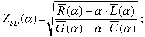
- the SD line impedance, Z SD ( ⁇ ); may also be experimentally determined for a test transmission line by measuring the SD portion of the voltage waveform across various known, termination impedances and computing the value Z SD ( ⁇ ) from the measurements.
- the measured SD waveform at a termination, V SD (R t ) consists of the sum of the incident SD waveform, V SD + , and a reflected SD wave.
- the reflected wave is the product of the SD reflection coefficient, r, and the incident wave.
- the experimental setup used to determine Z SD from line measurements is shown in FIG. 14 .
- the measured input and termination waveforms of the voltages for a 1002 ft of T1 line, are shown in FIG. 15A . These measurements were made with an ⁇ of 1.5x 10 6 1/sec and termination resistances of 49.5 ohms, 98.6 ohms and an open circuit.
- This example describes an alternate precision TOF measurement method of SD test pulses for higher loss, longer lines whose attenuation of the test pulses is so extensive that their amplitudes become too small as they travel down the line for a common threshold crossing measurement to be feasible.
- the time of flight measured at a constant voltage threshold becomes more difficult to estimate as the waveform is attenuated. This can be seen by examining the voltage traces along an approximately 6-kft, 24 AWG, fifty twisted wire pair, telephone cable (See FIG. 17 ). Three pairs of the fifty have been connected in series to generate an approximately 18-kft, cable with three equal length sections.
- the applied SD input waveform is De ⁇ t , with a D of 0.19 volts and an ⁇ of 3.5 ⁇ 10 5 / sec 1 . This ⁇ is approximately one tenth of the ⁇ used for the 2-kft T1 cable.
- the smaller ⁇ is required here to reduce the attenuation of the truncated SD leading edge of the propagating pulse over these longer distances as discussed in section two. This allows signal detection over longer distances.
- FIG. 17 shows the voltage traces measured at the input, ⁇ 6 kft, ⁇ 12 kft, and ⁇ 18 kft distances, and it also shows the preservation of shape of the SD region of the highly attenuated propagating waveform.
- the ⁇ 18 kft trace is corrected for the reflection from the open termination by dividing the measured waveform in half. The last two traces show that even with this smaller ⁇ , beyond 12,000 ft there is little or no SD signal above 0.19 volts. This is the value of the input SD waveform parameter D, thus there is little or no SD voltage threshold common to the input SD waveform and the SD waveforms at these longer distances.
- the first step in precisely measuring highly attenuated SD pulse time of flight is to detect the SD region of the propagating pulse, V(t), measured and recorded at the distance l along the cable. This is done by computing the / dt dV t V t of the measured pulse waveform. In the. SD cable. This is done by computing the ratio / dt dV t V t of the measured pulse waveform. In the SD region of the pulse, this ratio is ⁇ . The end of the SD region is then found by detecting the time that this ratio diverges from ⁇ . The ratio / dt 2 d 2 V t / dt dV t can also be used to detect the end of the SD region. In the SD region, this ratio is also ⁇ .
- the later ratio of the second and first derivative responds more quickly, but is also more susceptible to noise than the ratio of the first derivative and the signal.
- These ratios as a function of time are plotted in FIG. 18 for the SD waveform measured at 12-kft.
- the ratio of ⁇ n V x t ⁇ n t ⁇ n ⁇ 1 V x t ⁇ n ⁇ 1 t for any positive n will have this property.
- the ratio will converge on ⁇ as time progresses.
- This ratio diverges at the end of the SD region.
- the end of the estimated SD region can provide a good marker to determine the speed of light in the medium.
- the truncated SD leading edge of the pulse does not disperse, even with frequency dependent parameters.
- the high frequency components of the closing pulse do undergo dispersion. These fast, high frequency components tend to erode the end of the truncated SD region as the pulse propagates. At long distances, these high frequency components are also more highly attenuated so the amount of SD region erosion is not proportional to the distance traveled.
- the detected end of the SD region serves as an initial estimate of the pulse time of flight or the distance the wave has traveled and serves to define the region examined for more precise time of flight measurements in the next step.
- the attenuation of the truncated SD signal propagating a distance d was shown to be e ⁇ A sd ⁇ 1 ⁇ v sd ⁇ LC d .
- the parameter / LC 1 is commonly referred to as Vp and is given as a fraction of the speed of light in a vacuum.
- Vp time domain reflectometry
- the value of the ratio used in this analysis is 0.59. The reason for this can be seen in FIG. 19 .
- the input waveform is attenuated and time shifted assuming the end of the SD region of the traveling wave corresponds to the point of truncation of the initial SD waveform, ( FIG. 20 , top).
- the input waveform is then incrementally translated in time and attenuated based on each new estimated distance traveled. At each distance estimate, this shifted and attenuated input waveform is subtracted from the measured waveform. If there is no dc voltage offset and no noise, this difference will be zero in the SD region when the estimated distance is equal to the actual distance.
- FIG. 21 shows the calculated standard deviation of the difference of the shifted and attenuated input waveform and the SD waveform measured at the splice between the second and third twisted wire pairs as a function of estimated distance. The minimum occurs at an estimated distance of 12,216 ft.
- FIG. 22A shows the difference of the two waveforms and the variance of the difference of the waveforms at the minimum.
- FIG. 22A indicates that there is a five to ten millivolt differential dc offset between the two measuring points.
- FIG. 22B is presented to show how the variance has increased when the estimated distance is 38 ft longer than the distance associated with the minimum.
- TDR Time Domain Reflectometer
- a Time Domain Reflectometer is a test instrument used to find faults in transmission lines and to empirically estimate transmission line lengths and other parameters characterizing the line such as inductance per unit length, capacitance per unit length, resistance per unit length and conductance per unit length.
- a fundamental measurement in TDR test technology is the time of flight (TOF) of a test pulse generated by the instrument and applied to the line. This time of flight may be measured by timing the passage of the pulse detected at two locations along the line, referred to as Time Domain Transmission measurements (TDT). Or by Time Domain Reflection measurements which estimate the launch time of a pulse at one position and the subsequent return time of the pulse back to the same location after the pulse has been reflected from a fault or other impedance change some distance along the line.
- TOF time of flight
- TTT Time Domain Transmission measurements
- TDR technology A fundamental limitation in TDR technology is the poor accuracy of these TOF measurements in lossy, dispersive transmission lines.
- the relatively high TDR accuracy of TOF values obtainable in short low loss, low dispersion transmissions lines is possible only because the propagating test pulses keep their shape and amplitude in tact over the distances they travel during TOF measurements.
- dispersive, lossy long transmission lines the test pulses used in the art change shape, change amplitude and speed as they travel.
- the TOF measurements used in the art under these circumstances focus on estimating the emergence time of the leading profile of the test pulses. This part of the signature of test pulses used in the art has characteristically a low signal level and low signal slope making an accurate pulse emergence time measurement difficult to obtain.
- TDR technology for lossy, dispersive transmission lines by using a test pulse that contains a truncated SD signal in its leading edge.
- This truncated SD leading edge travels at a constant speed along these transmission lines without changing shape.
- the speed of propagation of this SD edge is a function of the line parameters and the SD signal parameter alpha and is controllable by changing alpha.
- the truncated SD leading edge of the test pulse will be attenuated as it travels along a lossy line.
- this rate of attenuation is also a function of the line parameters and the SD signal parameter alpha and is controllable by changing alpha.
- TDR time of flight and distance estimates
- the accuracy of the SD test waveform in a TDR application can be demonstrated by an example using the T1 cable, as discussed in examples 1 and 2.
- the two twisted wire pairs inside the T1 cable are connected in series to form a 2004 ft cable and the truncated SD signal is applied to the input.
- the voltage trace is measured at the splice of the two lines at 1002 ft. This can eliminate the need to correct for any line impedance mismatch at the point of measurement.
- the exponential coefficient ⁇ of the applied wave is 6.7x10 6 sec -1
- the SD parameters, A SD and v SD are obtained from the empirical transfer function analysis presented in example 2. Interpolating from the data of table I gives an A SD of 10.703x10 -3 ft -1 and a v SD of 6.276x10 8 ft/sec for this ⁇ .
- the first demonstration terminates the cable with an open circuit.
- the reflected coefficient of an open circuit is +1, which results in a positive reflection.
- FIG. 24 shows the voltage waveform measured at the 1002 ft point showing the forward traveling applied wave and the wave reflected from an open termination at the end of the cable.
- FIG. 25 shows the result of the measured reflected wave together with the applied wave time shifted and attenuated according to the procedure of example 4. The total distance traveled by the reflected wave is measured to be 2004 ft by this process, or exactly two times the 1002 ft length of this twisted wire pair section.
- FIGS. 26A-B show the constant threshold timing method result for TOF discussed in example 1.
- This method results in a time of flight of 3,203 nsec, which gives an estimated total distance traveled of 2010 ft. This results in an estimated twisted wire pair section length of 1005 ft, or 3 ft in error (+0.3%).
- the accuracy of this method may decline more in cases where the test pulse experiences even more attenuation. This level of attenuation may not generally occur in digital circuits.
- the maximum attenuation of digital signals in interconnects is generally less than one-half of the driving signal.
- the constant threshold TOF measurements with the SD wave should be preferably more accurate than current TDR methods using estimated time of emergence of the reflected pulses.
- FIG. 27 shows the voltage waveform measured at the 1002 ft point showing the forward traveling applied wave and the wave reflected from a short circuit termination at the end of the second twisted wire pair.
- FIG. 28 shows the result of the inverted reflected wave and the applied wave time shifted and attenuated according to the procedure of example 4. The total distance traveled is measured to be 2004 ft by this process, or exactly two times the 1002 ft twisted wire pair length.
- FIGS. 29A-B show the constant threshold timing method of estimating TOF discussed in example 1. This method results in a time of flight of 3,200 nsec, which gives an estimated total distance traveled of 2008 ft. This results in an estimated twisted wire pair section length of 1004 ft, or 2 ft in error (+0.2%).
- the utility of the SD waveform to the TDR process can be increased by using an empirical transfer function obtained with the use of a non-SD pulse applied to the line in a way similar to the process discussed in example 2.
- an experimental voltage pulse is generated by an arbitrary function generator connected to a single unterminated twisted wire pair from the T1 cable. This waveform is shown in FIGS. 30-31 (dotted).
- the same waveform can be applied by the signal generator to a variable resistor load substituted-for the 1002 ft twisted wire pair. The resistor is adjusted until the waveform approximates the shape and magnitude of the waveform applied by the arbitrary waveform generator to the twisted wire pair, see FIGS. 30-31 (solid).
- the waveform match is not exact because the resistor does not have the exact same frequency response as that of the twisted wire pair.
- a load resistance equal to the characteristic impedance, Z o , of the twisted wire pair results in a waveform that is closely matched to the waveform applied to the cable and has similar frequency content.
- the difference between the signal measured with the resistive load and the signal measured with the transmission line consists of the response of the transmission line to the applied signal and contains any reflected waves from impedance mismatches on the transmission line.
- This function shown in FIG. 32 , can be used to evaluate the reflected transmission line response to a SD pulse.
- the test signal applied to the line was similar to the type obtained form a commercial TDR instrument for testing communication cables with lengths ranging up to 5-kft.
- the measurements resulting from this test line voltage were used to obtain an empirical line transfer function.
- the SD TOF and the line distance estimates were all obtained computationally by simulating the SD propagation along the line utilizing this empirical line transfer function estimated with non-SD signals.
- the SD waveform has several properties that make it suitable as the basis for a data transmission scheme. For example: the exponential shape is maintained as it propagates at constant speed in a uniform cable; the attenuation of the SD waveform is adjustable by changing the exponential waveform parameter ⁇ ; the propagating speed of the SD waveform is adjustable by changing the exponential waveform parameter ⁇ ; and the SD waveforms with different ⁇ 's are linearly independent.
- This example teaches using the first property as the basis for a method of transmitting data using SD waveforms.
- the signals are transmitted 2004 ft along a transmission line consisting of the two twisted wire pairs in a 1002 ft T1 cable connected in series.
- the second twisted wire pair is terminated with a 100-ohm resistor.
- the data is encoded on four SD waveforms, each having a distinct ⁇ .
- Each waveform can be transmitted with a positive or a negative D, resulting in eight total states for three bits per symbol.
- One symbol is transmitted every three microseconds, giving a data rate of 1 Mbps.
- several other communication schemes can be readily derived from the teachings contained herein.
- the symbols can consist of a two-microsecond truncated SD leading edge period followed by a one-microsecond recovery period.
- This recovery period includes a variable width half-sine compensating pulse adjusted to shorten the time required for the transmission line to return to a zero voltage.
- the need for this recovery period and compensating pulse is illustrated in FIGS. 36A-B and FIGS. 37A-B.
- FIG. 36A shows the transmitted pulse without the compensating pulse
- FIG. 36B shows the received pulse without the compensating pulse.
- the truncated SD waveform in the leading edge of the input pulse is closed with a simple ramp signal, which is rounded due to the line response.
- FIGS. 37A - B show the effect of the compensating pulse in eliminating this inter-symbol interference.
- Each truncated SD waveform may requires a different amount of compensation so the width of the half-sine pulse can be varied based on observing the pulse at the terminated end of the second twisted wire pair.
- FIG. 38 shows a series of four symbols applied to the twisted wire pair input. Each symbol has a unique ⁇ , and a unique D.
- the ⁇ 's are equally spaced 1.1x10 6 sec -1 apart at 2.2x10 6 sec -1 , 3.3x10 6 sec -1 , 4.4x10 6 sec -1 , and 5.5x10 6 sec -1 .
- the order ⁇ 's used for this illustration of four successive symbols in FIG. 9.3 is 4.4x10 6 sec -1 , 2.2x10 6 sec -1 , 3.3x10 6 sec -1 , and 5.5x10 6 sec -1 .
- the D's were chosen to maintain an approximately equal maximum and minimum symbol voltage. For this demonstration, the fourth waveform is inverted.
- FIG. 39 The signal measured at the 100-ohm termination at a distance of 2004-ft is shown in FIG. 39 .
- FIG. 40 shows the natural log of the signal within each symbol period for the signal of FIG. 39 .
- a set of matched filters could be used to detect the individual ⁇ 's.
- the slopes of the least square linear fits of the linear regions of these waveforms are shown in Table II (set forth below).
- the decision level for this demonstration would be one half of the step size in ⁇ (1.1x10 6 sec -1 ) of 0.55x10 6 sec - 1 All errors are well below this threshold.
- This example discusses using the fourth SD waveform property, that SD waveforms with different ⁇ 's are linearly independent.
- This property can be utilized to generate an orthogonal set of pulses. Data can be encoded on these pulses by varying their amplitude. These amplitude-modulated orthogonal pulses are transmitted simultaneously on the transmission line. At the receiver, the individual pulse amplitudes are computed by taking advantage of their orthogonality. The basic pulses derived from the SD waveforms must be orthogonal at the receiver for this scheme to work.
- the repetitive transmission of data may require closed pulses.
- closed pulses As shown in example 6, that the SD portion of the leading edge of a closed propagating pulse maintains its shape, while the shape used to close the pulse will disperse as it propagates.
- the attenuation and propagation speed of the truncated SD leading region of the pulse is a function of the SD parameter ⁇ . Therefore, the orthogonality of a set of these pulses with a variety of ⁇ values will be reduced as the pulses propagate. Fortunately, the pulses only have to be orthogonal at the receiver. Techniques can be used to generate a set of orthogonal pulses from linearly independent component pulses. The effect of the transmission line on these component pulses can be determined empirically.
- the five waveforms are shown for a seven-microsecond interval in FIG. 41 .
- the waveforms are linearly independent on this time interval.
- these SD waveforms have a polynomial structure, i.e. each waveform is equal to e ( ⁇ ) ⁇ t times the previous waveform.
- the waveforms show the trailing effects of dispersion beyond the 12 ⁇ sec symbol period, see FIG. 44 . If the spread of the pulses into the following symbol periods is not removed, this inter-symbol interference at the receiver will render data encoded at the transmitter unreadable.
- the compensation pulse, C(t) is one cycle of 1 ⁇ cos ⁇ 2.9 ⁇ 10 ⁇ 6 ⁇ t delayed one microsecond after the start of the symbol period, see FIG. 45.
- FIGS. 46 , 47 show the waveforms at the input and at 8 kft with appropriately sized compensating pulses added to each signal. The duration of these compensated component pulses at the receiver are now shorter than the desired 12 ⁇ sec symbol period (see FIG. 47 ), so any linear combination of these pulses will not interfere with the next symbol.
- the PCD method is preferable because it takes into account the entire inner-product space spanned by all of the components.
- the process makes use of the eigenvectors of the entire inner-product space to generate the transformation matrix.
- the transformation matrix can be easily manipulated to order the eigenvalues. In this example the four largest eigenvalues were selected by truncating the transformation matrix.
- This process yields a transformation matrix, B , that generates four waveforms that are orthonormal at 8-kft by linearly combining the five component signals. These waveforms are shown in FIG. 48 (the transmitted signals) and FIG. 49 (the received orthogonal signals).
- the orthonormal set S is orthogonal and normalized at the receiver.
- the process accounts for the effects of the channel and allows the transmitter input waveforms to be easily constructed as a linear combination of defined components prior to transmission.
- This set S can be used as the basis functions for an orthogonal pulse amplitude modulation data transmission scheme. This process is depicted in FIG. 50 .
- the data can be encoded by amplitude modulation with five bits on each of the four orthonormal pulses, S.
- Five bits requires thirty-two states. Each state corresponds to one amplitude level, a i , on each orthogonal pulse, S i .
- the amplitude levels were ⁇ 0.5, ⁇ 1.5, ... ⁇ 15.5.
- the symbol is transmitted and decoded at the receiver by using the orthogonality of the pulses.
- the applied signal on orthogonal pulse one can be found by taking the inner product of the symbol, Q, with the pulse one signal, S 1 . This is done by multiplying the received symbol by the known orthogonal pulse, integrating over the symbol period, and normalizing the result.
- FIG. 51 shows three successive symbols at the output of the transmitter and FIG. 52 shows the same three symbols at the input of the receiver.
- FIG. 53 is a histogram of the error in detected level, a expected -a detected , for one second, or 1.67x10 6 bits, of data transmitted with -140 dBm additive white gaussian noise (AWGN) present [7].
- the standard deviations of the error distributions are 0.016, 0.018, 0.020, and 0.018 with maximum detected errors of 0.074, 0.071, 0.083, and 0.078.
- the decoding amplitude decision level is ⁇ 0.5.
- This example teaches the use of SD waveforms in digital circuits, specifically, in on-chip clock circuits.
- On-chip clock circuits may behave like transmission lines with the increased clock rates.
- a major design advantage of the SD waveforms when used as clock signals is that the delay in an RC line RC / ⁇ ⁇ l is linear with length, l, instead of quadratic with length as it is with the commonly assumed step signal. Linear delay with length LC 1 + R L ⁇ ⁇ l is also true for the SD signal in an RLC line. In contrast, the delay in RLC transmission lines excited by a conventional signal exhibit an exponentially growing increase in delay with length [8].
- Time Skew Clock control is a major issue limiting system performance.
- a solution to this problem includes equalizing conductor lengths to the various locations on the chip where the clock signal is needed.
- Several geometrical patterns are commonly used (H, etc.) to equalize the signal path lengths, thereby equalizing signal delays. This requires equalizing the path lengths along the traces delivering the clock signal to pin locations that are physically close to the master chip clock driver with those clock signal path lengths to pin locations at the longest distances from the master driver.
- Small adjustments to equalize the delays may be accomplished by adjusting the line widths to modify the line parameters and thereby the delay per unit length and alternatively by active means such as varying the delay of delayed-locked loops embedded in the clock lines.
- the invention provides a method and/or apparatus for utilizing truncated SD clock waveforms to reduce the clock skew.
- An advantage of the invention is that the delay per unit length can be adjusted with the exponential coefficient, ⁇ , chosen in the clock line driver design. This controllable delay per unit length has been demonstrated for a 100-ft coaxial cable in the initial patent application [9]. The minimum coaxial cable delay measured was increased by a factor of 1.8.
- an SD waveform driver may also be made to create an SD clock signal with adjustable delay by including a mechanism for adjusting the exponential coefficient ⁇ in the clock generator. This adjustable delay of the SD clock signal may provide a larger delay adjustment range than the delayed-locked loops utilized in the current technology.
- the invention can include transmission media.
- the invention can include a method and/or apparatus for a time domain reflectometer. Further, the invention can include a method and/or apparatus for high-speed communication over a transmission line.
- the invention can also include a method and/or apparatus for high-speed clock signals in an integrated circuit.
- a or an, as used herein, are defined as one or more than one.
- the term plurality, as used herein, is defined as two or more than two.
- the term another, as used herein, is defined as at least a second or more.
- the terms including and/or having, as used herein, are defined as comprising (i.e., open language).
- the term coupled, as used herein, is defined as connected, although not necessarily directly, and not necessarily mechanically.
- the term approximately, as used herein, is defined as at least close to a given value (e.g., preferably within 10% of, more preferably within 1% of, and most preferably within 0.1% of).
- substantially is defined as at least approaching a given state (e.g., preferably within 10% of, more preferably within 1% of, and most preferably within 0.1% of).
- means as used herein, is defined as hardware, firmware and/or software for achieving a result.
- program or phrase computer program as used herein, is defined as a sequence of instructions designed for execution on a computer system.
- a program, or computer program may include a subroutine, a function, a procedure, an object method, an object implementation, an executable application, an applet, a servlet, a source code, an object code, a shared library/dynamic load library and/or other sequence of instructions designed for execution on a computer system.
Landscapes
- Engineering & Computer Science (AREA)
- Computer Networks & Wireless Communication (AREA)
- Signal Processing (AREA)
- Physics & Mathematics (AREA)
- Mathematical Physics (AREA)
- Theoretical Computer Science (AREA)
- General Physics & Mathematics (AREA)
- Power Engineering (AREA)
- Dc Digital Transmission (AREA)
- Measurement Of Resistance Or Impedance (AREA)
- Monitoring And Testing Of Transmission In General (AREA)
Claims (48)
- Ein Verfahren umfassend:Anlegen einer Eingangswellenform an ein Übertragungsmedium, wobei die Eingangswellenform eine Vorderflanke aufweist, die durch den Ausdruck De αt charakterisiert ist, wobei D eine Konstante ungleich Null ist, α eine Konstante ungleich Null ist und t die Zeit ist;Aufzeichnen der Eingangswellenform;Aufzeichnen einer Ausgangswellenform, wobei die Ausgangswellenform durch das Übertragungsmedium in Reaktion auf die Eingangswellenform erzeugt wird;Bestimmen einer Sequenz von Laufzeitwerten (time-of-flight values) zwischen der aufgezeichneten Eingangswellenform und der aufgezeichneten Ausgangswellenform, wobei jeder der Laufzeitwerte (time-of-flight values) durch Subtrahieren einer Zeit t1(Y) von einer Zeit t2(Y) bestimmt wird, wobei die Zeit t1(Y) die Zeit ist, wenn die Vorderflanke der Eingangswellenform einen Schwellenwertsignalpegel überschreitet, wobei die Zeit t2(Y) die Zeit ist, wenn eine Vorderflanke der Ausgangswellenform den Schwellenwertsignalpegel überschreitet, wobei jeder der Laufzeitwerte (time-of-flight values) unter Verwendung eines anderen Wertes des Schwellenwertsignalpegels Y bestimmt wird; undBerechnen eines Mittelwerts der Laufzeitwerte (time-of-flight values), um einen mittleren Laufzeitwert (time-of-flight value) zu bestimmen.
- Das Verfahren nach Anspruch 1, wobei die Eingangswellenform an das Übertragungsmedium an einer ersten Stelle angelegt wird, wobei die Ausgangswellenform an einer zweiten Stelle des Übertragungsmediums aufgezeichnet wird und das Verfahren ferner das Berechnen einer Entfernung zwischen der ersten Stelle und der zweiten Stelle auf der Grundlage des mittleren Laufzeitwerts (time-of-flight value) und einer bekannten Ausbreitungsgeschwindigkeit umfasst.
- Das Verfahren nach Anspruch 1, wobei die Ausgangswellenform aufgrund einer Impedanzdiskontinuität in dem Übertragungsmedium einer Reflexion entspricht und das Verfahren ferner das Berechnen einer Entfernung zu der Impedanzdiskontinuität auf der Grundlage des mittleren Laufzeitwerts (time-of-flight value) und einer bekannten Ausbreitungsgeschwindigkeit umfasst.
- Das Verfahren nach Anspruch 3, wobei das Übertragungsmedium eine elektrische Übertragungsleitung ist, wobei die Impedanzdiskontinuität an einem Ende der elektrischen Übertragungsleitung auftritt.
- Das Verfahren nach Anspruch 1, ferner umfassend:Berechnen einer Ausbreitungsgeschwindigkeit VSD(α) auf der Grundlage des mittleren Laufzeitwerts (time-of-flight value) und einer Länge des Übertragungsmediums.
- Das Verfahren nach Anspruch 5, das ferner das Berechnen eines räumlichen Dämpfungskoeffizienten ASD(α) auf der Grundlage der berechneten Ausbreitungsgeschwindigkeit VSD(α) und der Konstanten α, die ungleich Null ist, nach der Beziehung ASD(α) = α / VSD(α) umfasst.
- Das Verfahren nach Anspruch 2, ferner umfassend:Anlegen einer zweiten Eingangswellenform an ein zweites Übertragungsmedium, wobei die zweite Eingangswellenform eine Vorderflanke aufweist, die proportional ist zu eαt ;Messen einer Umlauflaufzeit (round trip time-of-flight) zwischen der zweiten Eingangswellenform und einer reflektierten Wellenform aufgrund einer Impedanzdiskontinuität in dem zweiten Übertragungsmedium; undBerechnen einer Entfernung zu der Impedanzdiskontinuität auf der Grundlage der Umlauflaufzeit (round trip time-of-flight) und der Ausbreitungsgeschwindigkeit v.
- Das Verfahren nach Anspruch 1, das ferner das Steuern der Impedanz der Übertragungsleitung durch die Wahl eines Exponential-Koeffizienten α umfasst.
- Das Verfahren nach Anspruch 1, ferner umfassend
Berechnen einer Sequenz an Varianzwerten, die jeweils auf einer Sequenz an Kandidaten-Laufzeitwerten (candidate time-of-flight values) basieren, wobei jeder der Varianzwerte berechnet wird durch:Dämpfen und Zeitversetzen der Eingangswellenform auf der Grundlage des entsprechenden Kandidaten-Laufzeitwertes (candidate time-of-flight value); undBerechnen einer Differenz zwischen der gedämpften und zeitversetzten Wellenform und der Ausgangswellenform, um ein Differenzsignal zu erhalten; undBerechnen einer Varianz des Differenzsignals;Minimierung der Varianz in Bezug auf die Laufzeit (time-of-flight) unter Verwendung der Sequenz an Varianzwerten, um eine verfeinerte Laufzeitschätzung (time-of-flight estimate) zu bestimmen. - Das Verfahren nach Anspruch 1, das ferner das Erzeugen eines Satzes an Impulsen umfasst, die lineare Kombinationen der exponentiellen Wellenformen umfassen.
- Das Verfahren nach Anspruch 10, wobei der Satz an Impulsen an einem Empfänger orthogonal ist.
- Das Verfahren nach Anspruch 11, wobei die Daten in jedem Satz an Impulsen durch Variieren jeder Impulsamplitude kodiert sind.
- Das Verfahren nach Anspruch 11, das ferner das Übertragen einer linearen Kombination aus dem Satz an Impulsen an einen Empfänger über das Übertragungsmedium umfasst.
- Das Verfahren nach Anspruch 1, ferner umfassend:Auswählen eines Satzes an Amplitudenpegeln {ai} basierend auf einem Satz an Eingangsdatenbits, die zu kodieren sind;Erzeugen eines Sendesymbols durch Berechnen einer linearen Kombination eines Satzes an Wellenformen {Si} unter Verwendung des Satzes an Amplitudenpegeln {ai}, wobei der Satz an Wellenformen {Si} mit einem Satz an Wellenformen {Zi} über eine Matrix B in Beziehung steht, wobei der Satz an Wellenformen {Zi} mit einem Satz an Wellenformen {Y'i} und einem Kompensationsimpuls C durch den Ausdruck Z = Y'+ bC in Beziehung steht, wobei b ein Koeffizientenvektor ist, wobei der Satz an Wellenformen {Y'i} mit einem Satz an Wellenformen {X'i} über eine Matrix A in Beziehung steht, wobei der Satz an Wellenformen {X'i} gleich {W(t)X1(t), W(t)X2(t), ..., W(t)XN(t)} ist, wobei N eine ganze Zahl größer oder gleich zwei ist, wobei X1(t), X2(t), ..., XN(t) Wellenformen sind, die exponentielle Vorderflanken aufweisen, wobei W(t) ein sinusförmiger Fensterimpuls ist;Übertragen des Symbols auf das Übertragungsmedium.
- Das Verfahren nach Anspruch 14, ferner umfassend:Übertragen eines Kompensationsimpuls C an einen Empfänger über das Übertragungsmedium;Übertragen des Satzes an Wellenformen {Y'i} an den Empfänger durch das Übertragungsmedium;Empfangen der Matrix B und des Vektors b von dem Empfänger, wobei die Matrix B und des Vektors b so konfiguriert sind, dass die Wellenformen des Satzes {Si} am Empfänger zueinander orthogonal sind.
- Das Verfahren nach Anspruch 1, ferner umfassend:Empfangen eines Kompensationsimpulses C von einem Sender über das Übertragungsmedium;Empfangen eines Satzes an Wellenformen {Y'i} von dem Sender über das Übertragungsmedium;Erzeugen eines Satzes an Wellenformen {Zi} aus dem Satz {Y'i} auf der Grundlage der Beziehung Z=Y'+bC, wobei b ein konstanter Vektor ist, wobei das Erzeugen des Satzes an Wellenformen das Auswählen des konstanten Vektors b umfasst, so dass die Zeitdauern der Wellenformen {Zi} kleiner sind als eine Symbolperiode; (siehe Beschreibung auf Seite 37, Zeile 18 bis Seite 38 Zeile 6)Erzeugen eines Satzes an zueinander orthogonalen Wellenformen {Si} aus dem Satz {Zi}, wobei die Erzeugung des Satzes an zueinander orthogonalen Wellenformen {Si} eine Matrix B erzeugt, die den Satz {Si} dem Satz {Zi} zuordnet;Senden der Matrix B an den Sender.
- Das Verfahren nach Anspruch 16, ferner umfassend:Empfangen eines Symbols Q von dem Übertragungsmedium;Berechen der inneren Produkte {<Q,Si>} zwischen dem Symbol Q und den Wellenformen des Satzes {Si};Normalisierten der inneren Produkte um normalisierte Amplitudenwerten zu bestimmen;Dekodieren der Informationen von den normalisierten Amplitudenwerten.
- Das Verfahren nach Anspruch 1, das ferner das Ausgleichen einer Taktausbreitungsverzögerung umfasst.
- Das Verfahren nach Anspruch 18, das ferner das Reduzieren eines Taktversatzes umfasst.
- Das Verfahren nach Anspruch 1, ferner umfassend:Berechnen eines Dämpfungswertes, der ein Verhältnis von einer maximalen Amplitude der Ausgangswellenform zu einer maximalen Amplitude der Eingangswellenform darstellt, wobei der Dämpfungswert basierend auf dem folgenden Ausdruck berechnet wird:
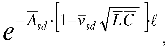
wobei ℓ eine Ausbreitungsstrecke in dem Übertragungsmedium ist,
wobeiL eine Induktivität pro Längeneinheit des Übertragungsmediums darstellt, wobeiC eine Kapazität pro Längeneinheit des Übertragungsmediums darstellt, wobei
und
wobeiR ein Widerstand pro Längeneinheit des Übertragungsmediums darstellt, wobeiG eine Leitfähigkeit pro Längeneinheit des Übertragungsmediums darstellt. - Verfahren nach Anspruch 1, wobei das Übertragungsmedium ein Paar an gekoppelten Übertragungsleitungen umfasst, wobei die Vorderflanke der Eingangswellenform bei einem maximalen Signalpegel zur Zeit ti abgeschnitten wird, wobei sich eine Dämpfung eines Signals an einem Punkt, tj , so dass 0 ≤ tj ≤ ti, der sich in dem Paar an gekoppelten Übertragungsleitungen ausbreitet wenn er bei einer Distanz ℓ in einem Bezugsrahmen t' gemessen wird, der sich mit einer Geschwindigkeit


wobeiL eine Induktivität pro Längeneinheit darstellt undC eine Kapazität pro Längeneinheit. - Das Verfahren nach Anspruch 1, wobei das Übertragungsmedium eine Single-Mode-Kommunikationsfaser ist, wobei das Anlegen der Eingangswellenform eine Ausbreitung eines optischen Impulses mit einer Hülle E(x,t) in einer Single-Mode-Kommunikationsfaser bewirkt, wobei die Vorderflanke der Eingangswellenform bei einem maximalen Signalpegel zu einem Zeitpunkt ti abgeschnitten wird, wobei sich eine Dämpfung der Hülle E(x,t) in einem Punkt, tj, so dass 0 ≤ tj ≤ ti, der sich in der Single-Mode-Kommunikationsfaser ausbreitet, wenn er bei einer Distanz ℓ in einem Referenzrahmen t' gemessen wird, der sich mit einer Gruppengeschwindigkeit 1/β1 ausbreitet, zu α gemäß der folgenden Gleichung verhält:

wobei T0=1/α und β3 ein Dispersionsparameter dritter Ordnung der optischen Single-Mode-Faser ist und γ ein Faserdämpfungsparameter ist. - Das Verfahren nach Anspruch 1, wobei das Übertragungsmedium eine Single-Mode-Kommunikationfaser ist, wobei das Anlegen der Eingangswellenform eine Ausbreitung einer Signalhülle innerhalb der Single-Mode-Kommunikationsfaser bewirkt, wobei das Verfahren ferner das Berechnen einer Ausbreitungsgeschwindigkeit Vsd(T0) einer Vorderflanke des Signals gemäß der folgenden Gleichung umfasst:

wobei T0=1/α, wobei 1/β1 eine Gruppengeschwindigkeit ist, wobei β3 ein Dispersionparameter dritter Ordnung der Single-Mode-Kommunikationsfaser ist und wobei γ ein Faserdämpfungsparameter der Single-Mode-Kommunikationsfaser ist. - Das Verfahren nach Anspruch 1, wobei das Übertragungsmedium eine Single-Mode-Kommunikations-Faser ist, wobei das Anlegen der Eingangswellenform die Ausbreitung eines Signalhülle innerhalb der Single-Mode-Kommunikationsfaser bewirkt, wobei das Verfahren ferner das Berechnen eines Dämpfungsparameters Asd(T0) der Signalhülle gemäß der folgenden Gleichung umfasst:

wobei T0=1/α, wobei 1/β1 eine Gruppengeschwindigkeit ist, wobei β3 ein Dispersionparameter dritter Ordnung der Single-Mode-Kommunikationsfaser ist und wobei γ ein Faserdämpfungsparameter der Single-Mode-Kommunikationsfaser ist. - Das Verfahren nach Anspruch 1, wobei das Übertragungsmedium eine elektrische Übertragungsleitung ist, wobei das Verfahren ferner das Berechnen einer Impedanz ZSD(α) der elektrischen Übertragungsleitung gemäß der folgenden Gleichung umfasst:

wobei L eine Induktivität pro Längeneinheit der elektrischen Übertragungsleitung darstellt, C eine Kapazität pro Längeneinheit der elektrischen Übertragungsleitung darstellt, R einen Widerstand pro Längeneinheit der elektrischen Übertragungsleitung darstellt und G eine Leitfähigkeit pro Längeneinheit der elektrischen Übertragungsleitung darstellt. - Das Verfahren nach Anspruch 1, wobei das Übertragungsmedium eine elektrische Übertragungsleitung ist, wobei das Verfahren ferner das Berechnen einer Impedanz ZSD(α) der elektrischen Übertragungsleitung gemäß der folgenden Gleichung umfasst:
wobeiL (s) eine Laplace-Transformation einer frequenzabhängigen Induktivität pro Längeneinheit der elektrischen Übertragungsleitung darstellt, wobeiL (α) istL (s) ausgewertet bei s=α, wobeiC (s) eine Laplace-Transformation einer frequenzabhängigen Kapazität pro Längeneinheit der elektrischen Übertragungsleitung darstellt, wobeiC (α) istC (s) ausgewertet bei s=α, wobeiR (s) eine Laplace-Transformation eines frequenzabhängigen Widerstands pro Längeneinheit der elektrischen Übertragungsleitung darstellt, wobeiR (α) istR (s) ausgewertet bei s=α und wobeiG (s) eine Laplace-Transformation einer frequenzabhängigen Leitfähigkeit pro Längeneinheit der elektrischen Übertragungsleitung darstellt, wobeiG (α) istG (s) ausgewertet bei s=α. - Das Verfahren nach Anspruch 1, wobei das Übertragungsmedium eine elektrische Übertragungsleitung ist.
- Das Verfahren nach Anspruch 1, wobei das Übertragungsmedium eine Single-Mode-Kommunikationsfaser ist.
- Das Verfahren nach Anspruch 1, wobei das Übertragungsmedium ein akustisches Medium ist.
- Das Verfahren nach Anspruch 1, wobei das Übertragungsmedium ein verlustbehaftetes Übertragungsmedium ist.
- Ein Verfahren umfassend:Anlegen eines Eingangsimpulses an ein Übertragungsmedium;Aufzeichnen des Eingangsimpulses;Aufzeichnen eines Antwortimpulses, das von dem Übertragungsmedium in Reaktion auf das Anlegen des Eingangsimpulses erzeugt wird;Berechnen einer Übertragungsfunktion des Übertragungsmediums basierend auf dem aufgezeichneten Eingangsimpuls und dem aufgezeichneten Antwortimpuls;Berechnen eines simulierten Antwortsignals unter Verwendung der Übertragungsfunktion und eines simulierten Eingangssignals, wobei das simulierte Eingangssignal eine Vorderflanke der Form Deαt aufweist, wobei D eine Konstante ungleich Null ist, wobei α eine Konstante ungleich Null ist, wobei t die Zeit ist;Berechnen einer Sequenz an Laufzeitwerten (time-of-flight values) zwischen dem simulierten Eingangssignal und dem simulierten Antwortsignal, wobei jeder der Laufzeitwerte (time-of-flight values) durch Subtrahieren einer Zeit t1(Y) von einer Zeit t2(Y) berechnet wird, wobei die Zeit t1(Y) die Zeit ist, wenn die Vorderflanke des simulierten Eingangssignals einen Schwellenwertsignalpegel Y überschreitet, wobei die Zeit t2(Y) die Zeit ist, wenn eine Vorderflanke des simulierten Antwortsignals den Schwellenwertsignalpegel Y überschreitet, wobei jeder der Laufzeitwerte (time-of-flight values) unter Verwendung eines unterschiedlichen Wertes des Schwellenwertsignalpegels Y berechnet wird; undBerechnen eines Mittelwerts der Laufzeitwerte (time-of-flight values).
- Das Verfahren nach Anspruch 31, wobei der Eingangsimpuls an einer ersten Stelle des Übertragungmediums angelegt wird, wobei der Antwortimpuls an einer zweiten Stelle des Übertragungsmediums aufgezeichnet wird und das Verfahren ferner das Berechnen einer Entfernung zwischen der ersten Stelle und der zweiten Stelle des Übertragungsmediums auf der Grundlage des mittleren Laufzeitwerts (time-of-flight value) und einer bekannten Ausbreitungsgeschwindigkeit in dem Übertragungsmedium umfasst.
- Das Verfahren nach Anspruch 31, wobei der Antwortimpuls durch eine Reflexion an einer Impedanzdiskontinuität in dem Übertragungsmedium erzeugt wird und das Verfahren ferner das Berechnen einer Entfernung zu der Impedanzdiskontinuität innerhalb des Übertragungsmediums auf der Grundlage des mittleren Laufzeitwerts (time-of-flight value) und einer bekannten Ausbreitungsgeschwindigkeit in dem Übertragungsmedium umfasst.
- Das Verfahren nach Anspruch 31, das ferner das Berechnen einer Ausbreitungsgeschwindigkeit vSD auf der Grundlage der mittleren Laufzeit (time-of-flight) und einer bekannten Länge umfasst, die mit dem Übertragungsmedium in Verbindung steht.
- Das Verfahren nach Anspruch 34, das ferner das Berechnen eines räumlichen Schwächungskoeffizienten ASD basierend auf dem Ausdruck ASD=α/VSD umfasst.
- Das Verfahren nach Anspruch 34, ferner umfassend:Wiederholen eines Satzes an Operationen einschließlich des Berechnens des simulierten Antwortsignals, des Berechnens der Sequenz an Laufzeitwerten (flight-of-time values) und des Berechnens des Mittelwertes, wobei jede der Wiederholungen einen anderen Wert für die Konstante α, die ungleich Null ist, benutzt;Berechnen einer Ausbreitungsgeschwindigkeit für jede der Wiederholungen auf der Grundlage des entsprechenden Mittelwerts und der bekannten Länge.
- Das Verfahren nach Anspruch 31, wobei das Berechnen der Übertragungsfunktion das Teilen einer Fourier-Transformation des Antwortimpulses durch eine Fourier-Transformation des Eingangsimpulses umfasst.
- Das Verfahren nach Anspruch 31, wobei das Übertragungsmedium eine verlustbehaftetes Übertragungsmedium ist.
- Ein Verfahren umfassend:Anlegen eines Eingangsimpulses an ein erstes Ende eines Übertragungsmediums;Aufzeichnen eines ersten Signals, das an dem ersten Ende des Übertragungsmediums auftritt, wobei das erste Signal eine Kombination aus dem Eingangsimpuls und einem reflektierten Impuls umfasst, wobei der reflektierte Impuls durch das Übertragungsmedium in Reaktion auf das Anlegen des Eingangsimpuls erzeugt wird;wiederholtes Anlegen des Eingangsimpulses auf eine variable Widerstandslast und Aufzeichnen eines zweiten Signals, das an der variablen Widerstandslast auftritt;Verändern des Widerstands der variablen Widerstandslast bis das aufgezeichnete zweite Signal dem aufgezeichneten ersten Signals in etwa entspricht;Berechnen einer Übertragungsfunktion des Übertragungsmediums auf der Grundlage des aufgezeichneten ersten Signals und des aufgezeichneten zweiten Signals, das dem aufgezeichneten erste Signal in etwa entspricht;Berechnen eines simulierten Antwortsignal unter Verwendung der Übertragungsfunktion und eines simulierten Eingangssignals, wobei das simulierte Eingangssignal eine Vorderflanke der Form Deαt aufweist, wobei D eine Konstante ungleich Null ist, wobei α eine Konstante ungleich Null ist, wobei t die Zeit ist;Berechnen einer Sequenz an Laufzeitwerten (time-of-flight values) zwischen dem simulierten Eingangssignal und dem simulierten Antwortsignal, wobei jeder der Laufzeitwerte (time-of-flight values) durch Subtrahieren einer Zeit t1(Y) von einer Zeit t2(Y) berechnet wird, wobei die Zeit t1(Y) die Zeit ist, wenn die Vorderflanke des simulierten Eingangssignals einen Schwellenwertsignalpegel Y überschreitet, wobei die Zeit t2(Y) die Zeit ist, wenn eine Vorderflanke des simulierten Antwortsignals den Schwellenwertsignalpegel Y überschreitet, wobei jeder der Laufzeitwerte (time-of-flight values) unter Verwendung eines anderen Wertes des Schwellensignalpegels Y berechnet wird; undBerechnen eines Mittelwerts der Laufzeitwerte (flight-of-time values).
- Das Verfahren nach Anspruch 39, wobei der reflektierte Impuls eine Reflexion eines Fehlers in dem Übertragungsmedium ist.
- Das Verfahren nach Anspruch 39, wobei das Übertragungsmedium ein verlustbehaftetes Übertragungsmedium ist.
- Eine Vorrichtung, umfassend:einen Wellenformgenerator, der konfiguriert ist, um eine Eingangswellenform zu erzeugen, die eine Vorderflanke gekennzeichnet durch den Ausdruck Deαt aufweist, wobei D eine Konstante ungleich Null ist, α eine Konstante ungleich Null ist und t die Zeit ist;einen Eingangsrekorder, der konfiguriert ist, um die Eingangswellenform aufzuzeichnen;eine Ausgangsrekorder, der konfiguriert ist, um eine Ausgangswellenform, die von einem Übertragungsmedium in Reaktion auf die Eingangswellenform, die an das Übertragungsmedium angelegt wird, erzeugt wird; undeinen Computer, der konfiguriert ist, um eine Sequenz an Laufzeitwerten (time-of-flight values) zwischen der aufgezeichneten Eingangswellenform und der aufgezeichneten Ausgangswellenform zu berechnen und um einen Mittelwert der Laufzeitwerte (time-of-flight values) zu berechnen, wobei jeder der Laufzeitwerte (time-of-flight values) durch Subtrahieren einer Zeit t1(Y) von einer Zeit t2(Y) berechnet wird, wobei t1(Y) die Zeit ist, wenn die Vorderflanke der Eingangswellenform einen Schwellenwertsignalpegel Y überschreitet, wobei t2(Y) die Zeit ist, wenn eine Vorderflanke der Ausgangswellenform den Schwellenwertsignalpegel Y überschreitet, wobei jeder der Laufzeitwerte (time-of-flight values) unter Verwendung eines anderen Wertes des Schwellensignalpegels Y berechnet wird.
- Die Vorrichtung nach Anspruch 42, wobei das Übertragungsmedium eine elektrische Übertragungsleitung ist, wobei die Vorrichtung ferner ein Übertragungsmedium-Verbinder zur Kopplung an die elektrische Übertragungsleitung umfasst, wobei der Wellenformgenerator, der Eingangsrekorder und der Ausgangsrekorder an den elektrischen Verbinder gekoppelt sind.
- Die Vorrichtung nach Anspruch 43, wobei die Ausgangswellenform einer Reflexion einer Impedanzdiskontinuität in der elektrischen Übertragungsleitung entspricht, wobei der Computer konfiguriert ist, um einen Abstand zur Impedanzdiskontinuität auf der Grundlage der mittleren Laufzeit und einer bekannten Ausbreitungsgeschwindigkeit in dem Übertragungsmedium zu berechnen.
- Die Vorrichtung nach Anspruch 42, wobei der Computer ferner konfiguriert ist, um eine Ausbreitungsgeschwindigkeit vSD auf der Grundlage der mittleren Laufzeit (time-of-flight) und einem Abstand zu berechnen, der mit dem Übertragungsmedium in Verbindung steht.
- Die Vorrichtung nach Anspruch 45, wobei der Computer ferner konfiguriert ist, um einen räumlichen Schwächungskoeffizienten ASD für das Übertragungsmedium nach dem Ausdruck ASD =α/vSD zu berechnen.
- Die Vorrichtung nach Anspruch 42, wobei das Übertragungsmedium eine Single-Mode-Kommunikationsfaser ist.
- Die Vorrichtung nach Anspruch 42, wobei das Übertragungsmedium ein verlustbehaftete Übertragungsmedium ist.
Applications Claiming Priority (3)
| Application Number | Priority Date | Filing Date | Title |
|---|---|---|---|
| US224541 | 1998-12-31 | ||
| US10/224,541 US6847267B2 (en) | 2000-03-07 | 2002-08-20 | Methods for transmitting a waveform having a controllable attenuation and propagation velocity |
| PCT/US2003/025979 WO2004019501A2 (en) | 2002-08-20 | 2003-08-19 | Methods for transmitting a waveform having a controllable attenuation and propagation velocity |
Publications (3)
| Publication Number | Publication Date |
|---|---|
| EP1540844A2 EP1540844A2 (de) | 2005-06-15 |
| EP1540844A4 EP1540844A4 (de) | 2009-12-23 |
| EP1540844B1 true EP1540844B1 (de) | 2016-04-13 |
Family
ID=31946278
Family Applications (1)
| Application Number | Title | Priority Date | Filing Date |
|---|---|---|---|
| EP03793136.7A Expired - Lifetime EP1540844B1 (de) | 2002-08-20 | 2003-08-19 | Verfahren zum senden einer signalform mit steuerbarer dämpfung und ausbreitungsgeschwindigkeit |
Country Status (6)
| Country | Link |
|---|---|
| US (1) | US6847267B2 (de) |
| EP (1) | EP1540844B1 (de) |
| JP (2) | JP5068933B2 (de) |
| AU (1) | AU2003259928A1 (de) |
| CA (2) | CA2833510C (de) |
| WO (1) | WO2004019501A2 (de) |
Families Citing this family (17)
| Publication number | Priority date | Publication date | Assignee | Title |
|---|---|---|---|---|
| US7724761B1 (en) * | 2000-03-07 | 2010-05-25 | Juniper Networks, Inc. | Systems and methods for reducing reflections and frequency dependent dispersions in redundant links |
| US7375602B2 (en) * | 2000-03-07 | 2008-05-20 | Board Of Regents, The University Of Texas System | Methods for propagating a non sinusoidal signal without distortion in dispersive lossy media |
| US20040218688A1 (en) * | 2002-06-21 | 2004-11-04 | John Santhoff | Ultra-wideband communication through a power grid |
| US20040156446A1 (en) * | 2002-06-21 | 2004-08-12 | John Santhoff | Optimization of ultra-wideband communication through a wire medium |
| US20060291536A1 (en) * | 2002-06-21 | 2006-12-28 | John Santhoff | Ultra-wideband communication through a wire medium |
| US7167525B2 (en) * | 2002-06-21 | 2007-01-23 | Pulse-Link, Inc. | Ultra-wideband communication through twisted-pair wire media |
| US6782048B2 (en) * | 2002-06-21 | 2004-08-24 | Pulse-Link, Inc. | Ultra-wideband communication through a wired network |
| US7398333B2 (en) * | 2003-08-27 | 2008-07-08 | Rambus Inc. | Integrated circuit input/output interface with empirically determined delay matching |
| US8269647B2 (en) * | 2006-02-15 | 2012-09-18 | Schlumberger Technology Corporation | Well depth measurement using time domain reflectometry |
| CN101501476B (zh) * | 2006-09-06 | 2013-03-27 | 国立大学法人横浜国立大学 | 无源互调失真的测定方法及测定系统 |
| US8867657B1 (en) | 2014-02-17 | 2014-10-21 | Board Of Regents, The University Of Texas System | Communication using analog pulses having exponentially-shaped leading edges |
| US9331842B2 (en) | 2014-09-23 | 2016-05-03 | Board Of Regents, The University Of Texas System | Time synchronization and controlled asynchronization of remote trigger signals |
| WO2017030474A1 (en) * | 2015-08-18 | 2017-02-23 | Telefonaktiebolaget Lm Ericsson (Publ) | Methods and devices for determining termination characteristics of an electrically conductive line |
| EP3363267B1 (de) | 2015-10-16 | 2019-11-20 | Signify Holding B.V. | Inbetriebnahme von lastvorrichtungen über challenge-response-timing |
| US10554299B2 (en) * | 2017-05-09 | 2020-02-04 | Huawei Technologies Co., Ltd. | Method and apparatus for characterizing a dispersion of an optical medium |
| FR3099830B1 (fr) * | 2019-08-06 | 2021-07-02 | Centralesupelec | Procédé et système de surveillance d’un réseau de câbles, par analyse en composantes principales |
| WO2021060558A1 (ja) * | 2019-09-27 | 2021-04-01 | 学校法人福岡大学 | 回路特性測定システム、及び回路特性測定方法 |
Family Cites Families (23)
| Publication number | Priority date | Publication date | Assignee | Title |
|---|---|---|---|---|
| FR2080068A5 (de) | 1970-02-23 | 1971-11-12 | Commissariat Energie Atomique | |
| CH549909A (de) | 1972-12-06 | 1974-05-31 | Siemens Ag Albis | Verfahren zur messung und/oder ueberwachung der uebertragungsqualitaet einer nachrichtenuebertragungsanlage. |
| US4176285A (en) | 1978-01-11 | 1979-11-27 | The United States Of America As Represented By The United States Department Of Energy | Electrical pulse generator |
| US4566084A (en) | 1982-09-30 | 1986-01-21 | The United States Of America As Represented By The United States Department Of Energy | Acoustic velocity measurements in materials using a regenerative method |
| US4559602A (en) | 1983-01-27 | 1985-12-17 | Bates Jr John K | Signal processing and synthesizing method and apparatus |
| PL139300B1 (en) | 1983-04-27 | 1987-01-31 | Pan Ct Badan Molekularnych I M | Method of determination of thermal conductivity and heat storage capacity of materials and apparatus therefor |
| EP0501722B1 (de) * | 1991-02-26 | 1998-04-29 | Nippon Telegraph And Telephone Corporation | Verfahren zur Messung der Länge einer Übertragungsleitung |
| JPH04285874A (ja) | 1991-03-13 | 1992-10-09 | Chubu Electric Power Co Inc | ケーブルの事故点標定方法 |
| US5142861A (en) | 1991-04-26 | 1992-09-01 | Schlicher Rex L | Nonlinear electromagnetic propulsion system and method |
| US5452222A (en) | 1992-08-05 | 1995-09-19 | Ensco, Inc. | Fast-risetime magnetically coupled current injector and methods for using same |
| US5544047A (en) * | 1993-12-29 | 1996-08-06 | International Business Machines Corporation | Reflective wave compensation on high speed processor cards |
| US5584580A (en) | 1994-02-24 | 1996-12-17 | Uniflex, Inc. | Tamper-resistant envelope closure |
| US5461318A (en) * | 1994-06-08 | 1995-10-24 | Borchert; Marshall B. | Apparatus and method for improving a time domain reflectometer |
| JPH08152474A (ja) * | 1994-09-28 | 1996-06-11 | Nikon Corp | 距離測定装置 |
| GB9502087D0 (en) | 1995-02-02 | 1995-03-22 | Croma Dev Ltd | Improvements relating to pulse echo distance measurement |
| US5686872A (en) | 1995-03-13 | 1997-11-11 | National Semiconductor Corporation | Termination circuit for computer parallel data port |
| US5650728A (en) | 1995-04-03 | 1997-07-22 | Hubbell Incorporated | Fault detection system including a capacitor for generating a pulse and a processor for determining admittance versus frequency of a reflected pulse |
| JP2688012B2 (ja) | 1995-05-12 | 1997-12-08 | 工業技術院長 | 熱拡散率測定方法 |
| JPH09197044A (ja) * | 1996-01-16 | 1997-07-31 | Mitsubishi Electric Corp | レーザ測距装置 |
| US5857001A (en) | 1997-02-10 | 1999-01-05 | International Business Machines Corporation | Off chip driver with precompensation for cable attenuation |
| US6097755A (en) * | 1997-10-20 | 2000-08-01 | Tektronix, Inc. | Time domain reflectometer having optimal interrogating pulses |
| US6922388B1 (en) * | 2000-02-11 | 2005-07-26 | Lucent Technologies Inc. | Signal construction, detection and estimation for uplink timing synchronization and access control in a multi-access wireless communication system |
| US6441695B1 (en) * | 2000-03-07 | 2002-08-27 | Board Of Regents, The University Of Texas System | Methods for transmitting a waveform having a controllable attenuation and propagation velocity |
-
2002
- 2002-08-20 US US10/224,541 patent/US6847267B2/en not_active Expired - Lifetime
-
2003
- 2003-08-19 JP JP2004531090A patent/JP5068933B2/ja not_active Expired - Fee Related
- 2003-08-19 EP EP03793136.7A patent/EP1540844B1/de not_active Expired - Lifetime
- 2003-08-19 CA CA2833510A patent/CA2833510C/en not_active Expired - Fee Related
- 2003-08-19 CA CA2496322A patent/CA2496322C/en not_active Expired - Fee Related
- 2003-08-19 WO PCT/US2003/025979 patent/WO2004019501A2/en not_active Ceased
- 2003-08-19 AU AU2003259928A patent/AU2003259928A1/en not_active Abandoned
-
2011
- 2011-12-28 JP JP2011288883A patent/JP5306445B2/ja not_active Expired - Fee Related
Also Published As
| Publication number | Publication date |
|---|---|
| EP1540844A2 (de) | 2005-06-15 |
| JP2012156994A (ja) | 2012-08-16 |
| AU2003259928A8 (en) | 2004-03-11 |
| JP2005536749A (ja) | 2005-12-02 |
| CA2496322A1 (en) | 2004-03-04 |
| US20030085771A1 (en) | 2003-05-08 |
| CA2833510A1 (en) | 2004-03-04 |
| AU2003259928A1 (en) | 2004-03-11 |
| JP5068933B2 (ja) | 2012-11-07 |
| CA2833510C (en) | 2016-10-11 |
| US6847267B2 (en) | 2005-01-25 |
| HK1078390A1 (zh) | 2006-03-10 |
| EP1540844A4 (de) | 2009-12-23 |
| WO2004019501A3 (en) | 2004-06-10 |
| WO2004019501A2 (en) | 2004-03-04 |
| JP5306445B2 (ja) | 2013-10-02 |
| CA2496322C (en) | 2014-10-14 |
Similar Documents
| Publication | Publication Date | Title |
|---|---|---|
| US7859271B2 (en) | Methods for propagating a non sinusoidal signal without distortion in dispersive lossy media | |
| JP5306445B2 (ja) | 制御可能な減衰と伝播速度とを有する波形を伝送する方法 | |
| Moini et al. | A new lightning return stroke model based on antenna theory | |
| US20180045761A1 (en) | Jitter and eye contour at ber measurements after dfe | |
| EP1358720B1 (de) | Verfahren zur übertragung einer wellenform mit steuerbarer dämpfung und ausbreitungsgeschwindigkeit | |
| CN101233714B (zh) | 补偿通信系统中的抖动的方法和系统 | |
| EP3158655B1 (de) | Schätzung von impedanzen in einem übertragungsmedium | |
| US8705601B2 (en) | Apparatus and method for varying inter symbol interference and bandwidth extension pre-emphasis on a high speed digital signal | |
| US5321365A (en) | Reduced noise sensitivity in inverse scattering through filtering | |
| HK1078390B (en) | Methods for transmitting a waveform having a controllable attenuation and propagation velocity | |
| US6407609B1 (en) | Distortion precompensator and method of compensating for distortion in a transmission medium | |
| US10185020B1 (en) | Method of compensating loss and dispersion of transmission line for time domain reflectometry | |
| US6566891B1 (en) | Measurement system and method of determining characteristics associated with a waveform having distortion associated therewith | |
| US20160087785A1 (en) | Time synchronization and controlled asynchronization of remote trigger signals | |
| US20070197169A1 (en) | Systems and methods for transmitter and channel characterization | |
| Matsuoka et al. | A high signal integrity interconnect design using a genetic algorithm and its solution analysis: What solution did GA find in time and frequency domain? | |
| Fuks et al. | Permittivity profile reconstructions using transient electromagnetic reflection data | |
| Biskup et al. | Flake et al.(45) Date of Patent: Dec. 28, 2010 | |
| Cain | Asynchronous Gb/s signaling for digital communication | |
| Bhattacharyya et al. | Impact on inter symbol interference (ISI) noise due to simulation error | |
| Wang et al. | A Method for Evaluation on Signal Integrity of SpaceWire High-Speed Transmission Network | |
| Luis Oslinger-Gutiérrez et al. | Analysis of the partial discharge pulse propagation in the stator winding of a synchronous machine. | |
| Elliott Cole | TIA/EIA-568A Category 5 cables in low-voltage differential signaling (LVDS) | |
| Sripada | Application of e-TDR to achieve precise time synchronization and controlled asynchronization of remotely located signals | |
| Daggett | Information Technology SCSI Passive Interconnect Performance (PIP) |
Legal Events
| Date | Code | Title | Description |
|---|---|---|---|
| PUAI | Public reference made under article 153(3) epc to a published international application that has entered the european phase |
Free format text: ORIGINAL CODE: 0009012 |
|
| 17P | Request for examination filed |
Effective date: 20050321 |
|
| AK | Designated contracting states |
Kind code of ref document: A2 Designated state(s): AT BE BG CH CY CZ DE DK EE ES FI FR GB GR HU IE IT LI LU MC NL PT RO SE SI SK TR |
|
| AX | Request for extension of the european patent |
Extension state: AL LT LV MK |
|
| DAX | Request for extension of the european patent (deleted) | ||
| RAP1 | Party data changed (applicant data changed or rights of an application transferred) |
Owner name: BOARD OF REGENTS, THE UNIVERSITY OF TEXAS SYSTEM |
|
| REG | Reference to a national code |
Ref country code: HK Ref legal event code: DE Ref document number: 1078390 Country of ref document: HK |
|
| RIN1 | Information on inventor provided before grant (corrected) |
Inventor name: FLAKE, ROBERT, H. Inventor name: BISKUP, JOHN, F. |
|
| A4 | Supplementary search report drawn up and despatched |
Effective date: 20091123 |
|
| 17Q | First examination report despatched |
Effective date: 20110223 |
|
| GRAP | Despatch of communication of intention to grant a patent |
Free format text: ORIGINAL CODE: EPIDOSNIGR1 |
|
| INTG | Intention to grant announced |
Effective date: 20150810 |
|
| GRAS | Grant fee paid |
Free format text: ORIGINAL CODE: EPIDOSNIGR3 |
|
| GRAA | (expected) grant |
Free format text: ORIGINAL CODE: 0009210 |
|
| AK | Designated contracting states |
Kind code of ref document: B1 Designated state(s): AT BE BG CH CY CZ DE DK EE ES FI FR GB GR HU IE IT LI LU MC NL PT RO SE SI SK TR |
|
| REG | Reference to a national code |
Ref country code: GB Ref legal event code: FG4D |
|
| REG | Reference to a national code |
Ref country code: AT Ref legal event code: REF Ref document number: 791096 Country of ref document: AT Kind code of ref document: T Effective date: 20160415 Ref country code: CH Ref legal event code: EP |
|
| REG | Reference to a national code |
Ref country code: IE Ref legal event code: FG4D |
|
| REG | Reference to a national code |
Ref country code: DE Ref legal event code: R096 Ref document number: 60348826 Country of ref document: DE |
|
| REG | Reference to a national code |
Ref country code: FR Ref legal event code: PLFP Year of fee payment: 14 |
|
| REG | Reference to a national code |
Ref country code: AT Ref legal event code: MK05 Ref document number: 791096 Country of ref document: AT Kind code of ref document: T Effective date: 20160413 |
|
| REG | Reference to a national code |
Ref country code: NL Ref legal event code: MP Effective date: 20160413 |
|
| PG25 | Lapsed in a contracting state [announced via postgrant information from national office to epo] |
Ref country code: FI Free format text: LAPSE BECAUSE OF FAILURE TO SUBMIT A TRANSLATION OF THE DESCRIPTION OR TO PAY THE FEE WITHIN THE PRESCRIBED TIME-LIMIT Effective date: 20160413 Ref country code: NL Free format text: LAPSE BECAUSE OF FAILURE TO SUBMIT A TRANSLATION OF THE DESCRIPTION OR TO PAY THE FEE WITHIN THE PRESCRIBED TIME-LIMIT Effective date: 20160413 |
|
| PG25 | Lapsed in a contracting state [announced via postgrant information from national office to epo] |
Ref country code: SE Free format text: LAPSE BECAUSE OF FAILURE TO SUBMIT A TRANSLATION OF THE DESCRIPTION OR TO PAY THE FEE WITHIN THE PRESCRIBED TIME-LIMIT Effective date: 20160413 Ref country code: PT Free format text: LAPSE BECAUSE OF FAILURE TO SUBMIT A TRANSLATION OF THE DESCRIPTION OR TO PAY THE FEE WITHIN THE PRESCRIBED TIME-LIMIT Effective date: 20160816 Ref country code: AT Free format text: LAPSE BECAUSE OF FAILURE TO SUBMIT A TRANSLATION OF THE DESCRIPTION OR TO PAY THE FEE WITHIN THE PRESCRIBED TIME-LIMIT Effective date: 20160413 Ref country code: ES Free format text: LAPSE BECAUSE OF FAILURE TO SUBMIT A TRANSLATION OF THE DESCRIPTION OR TO PAY THE FEE WITHIN THE PRESCRIBED TIME-LIMIT Effective date: 20160413 Ref country code: GR Free format text: LAPSE BECAUSE OF FAILURE TO SUBMIT A TRANSLATION OF THE DESCRIPTION OR TO PAY THE FEE WITHIN THE PRESCRIBED TIME-LIMIT Effective date: 20160714 |
|
| PG25 | Lapsed in a contracting state [announced via postgrant information from national office to epo] |
Ref country code: IT Free format text: LAPSE BECAUSE OF FAILURE TO SUBMIT A TRANSLATION OF THE DESCRIPTION OR TO PAY THE FEE WITHIN THE PRESCRIBED TIME-LIMIT Effective date: 20160413 Ref country code: BE Free format text: LAPSE BECAUSE OF FAILURE TO SUBMIT A TRANSLATION OF THE DESCRIPTION OR TO PAY THE FEE WITHIN THE PRESCRIBED TIME-LIMIT Effective date: 20160413 |
|
| REG | Reference to a national code |
Ref country code: DE Ref legal event code: R097 Ref document number: 60348826 Country of ref document: DE |
|
| PG25 | Lapsed in a contracting state [announced via postgrant information from national office to epo] |
Ref country code: SK Free format text: LAPSE BECAUSE OF FAILURE TO SUBMIT A TRANSLATION OF THE DESCRIPTION OR TO PAY THE FEE WITHIN THE PRESCRIBED TIME-LIMIT Effective date: 20160413 Ref country code: CZ Free format text: LAPSE BECAUSE OF FAILURE TO SUBMIT A TRANSLATION OF THE DESCRIPTION OR TO PAY THE FEE WITHIN THE PRESCRIBED TIME-LIMIT Effective date: 20160413 Ref country code: EE Free format text: LAPSE BECAUSE OF FAILURE TO SUBMIT A TRANSLATION OF THE DESCRIPTION OR TO PAY THE FEE WITHIN THE PRESCRIBED TIME-LIMIT Effective date: 20160413 Ref country code: RO Free format text: LAPSE BECAUSE OF FAILURE TO SUBMIT A TRANSLATION OF THE DESCRIPTION OR TO PAY THE FEE WITHIN THE PRESCRIBED TIME-LIMIT Effective date: 20160413 Ref country code: DK Free format text: LAPSE BECAUSE OF FAILURE TO SUBMIT A TRANSLATION OF THE DESCRIPTION OR TO PAY THE FEE WITHIN THE PRESCRIBED TIME-LIMIT Effective date: 20160413 |
|
| PLBE | No opposition filed within time limit |
Free format text: ORIGINAL CODE: 0009261 |
|
| STAA | Information on the status of an ep patent application or granted ep patent |
Free format text: STATUS: NO OPPOSITION FILED WITHIN TIME LIMIT |
|
| 26N | No opposition filed |
Effective date: 20170116 |
|
| PG25 | Lapsed in a contracting state [announced via postgrant information from national office to epo] |
Ref country code: MC Free format text: LAPSE BECAUSE OF FAILURE TO SUBMIT A TRANSLATION OF THE DESCRIPTION OR TO PAY THE FEE WITHIN THE PRESCRIBED TIME-LIMIT Effective date: 20160413 |
|
| REG | Reference to a national code |
Ref country code: CH Ref legal event code: PL |
|
| PG25 | Lapsed in a contracting state [announced via postgrant information from national office to epo] |
Ref country code: CH Free format text: LAPSE BECAUSE OF NON-PAYMENT OF DUE FEES Effective date: 20160831 Ref country code: LI Free format text: LAPSE BECAUSE OF NON-PAYMENT OF DUE FEES Effective date: 20160831 |
|
| PG25 | Lapsed in a contracting state [announced via postgrant information from national office to epo] |
Ref country code: SI Free format text: LAPSE BECAUSE OF FAILURE TO SUBMIT A TRANSLATION OF THE DESCRIPTION OR TO PAY THE FEE WITHIN THE PRESCRIBED TIME-LIMIT Effective date: 20160413 |
|
| REG | Reference to a national code |
Ref country code: IE Ref legal event code: MM4A |
|
| REG | Reference to a national code |
Ref country code: HK Ref legal event code: GR Ref document number: 1078390 Country of ref document: HK |
|
| PG25 | Lapsed in a contracting state [announced via postgrant information from national office to epo] |
Ref country code: IE Free format text: LAPSE BECAUSE OF NON-PAYMENT OF DUE FEES Effective date: 20160819 |
|
| REG | Reference to a national code |
Ref country code: FR Ref legal event code: PLFP Year of fee payment: 15 |
|
| PG25 | Lapsed in a contracting state [announced via postgrant information from national office to epo] |
Ref country code: LU Free format text: LAPSE BECAUSE OF NON-PAYMENT OF DUE FEES Effective date: 20160819 |
|
| PGFP | Annual fee paid to national office [announced via postgrant information from national office to epo] |
Ref country code: GB Payment date: 20170824 Year of fee payment: 15 Ref country code: FR Payment date: 20170823 Year of fee payment: 15 Ref country code: DE Payment date: 20170814 Year of fee payment: 15 |
|
| PG25 | Lapsed in a contracting state [announced via postgrant information from national office to epo] |
Ref country code: HU Free format text: LAPSE BECAUSE OF FAILURE TO SUBMIT A TRANSLATION OF THE DESCRIPTION OR TO PAY THE FEE WITHIN THE PRESCRIBED TIME-LIMIT; INVALID AB INITIO Effective date: 20030819 Ref country code: CY Free format text: LAPSE BECAUSE OF FAILURE TO SUBMIT A TRANSLATION OF THE DESCRIPTION OR TO PAY THE FEE WITHIN THE PRESCRIBED TIME-LIMIT Effective date: 20160413 |
|
| PG25 | Lapsed in a contracting state [announced via postgrant information from national office to epo] |
Ref country code: TR Free format text: LAPSE BECAUSE OF FAILURE TO SUBMIT A TRANSLATION OF THE DESCRIPTION OR TO PAY THE FEE WITHIN THE PRESCRIBED TIME-LIMIT Effective date: 20160413 |
|
| PG25 | Lapsed in a contracting state [announced via postgrant information from national office to epo] |
Ref country code: BG Free format text: LAPSE BECAUSE OF FAILURE TO SUBMIT A TRANSLATION OF THE DESCRIPTION OR TO PAY THE FEE WITHIN THE PRESCRIBED TIME-LIMIT Effective date: 20160413 |
|
| REG | Reference to a national code |
Ref country code: DE Ref legal event code: R119 Ref document number: 60348826 Country of ref document: DE |
|
| GBPC | Gb: european patent ceased through non-payment of renewal fee |
Effective date: 20180819 |
|
| PG25 | Lapsed in a contracting state [announced via postgrant information from national office to epo] |
Ref country code: DE Free format text: LAPSE BECAUSE OF NON-PAYMENT OF DUE FEES Effective date: 20190301 |
|
| PG25 | Lapsed in a contracting state [announced via postgrant information from national office to epo] |
Ref country code: FR Free format text: LAPSE BECAUSE OF NON-PAYMENT OF DUE FEES Effective date: 20180831 |
|
| PG25 | Lapsed in a contracting state [announced via postgrant information from national office to epo] |
Ref country code: GB Free format text: LAPSE BECAUSE OF NON-PAYMENT OF DUE FEES Effective date: 20180819 |