EP1540694B1 - Procede et appareil pour produire des taux de traitement uniformes - Google Patents
Procede et appareil pour produire des taux de traitement uniformes Download PDFInfo
- Publication number
- EP1540694B1 EP1540694B1 EP03765610.5A EP03765610A EP1540694B1 EP 1540694 B1 EP1540694 B1 EP 1540694B1 EP 03765610 A EP03765610 A EP 03765610A EP 1540694 B1 EP1540694 B1 EP 1540694B1
- Authority
- EP
- European Patent Office
- Prior art keywords
- antenna
- passive
- field
- plasma
- passive antenna
- Prior art date
- Legal status (The legal status is an assumption and is not a legal conclusion. Google has not performed a legal analysis and makes no representation as to the accuracy of the status listed.)
- Expired - Lifetime
Links
- 238000012545 processing Methods 0.000 title claims description 110
- 238000000034 method Methods 0.000 title claims description 36
- 238000009826 distribution Methods 0.000 claims description 95
- 230000001939 inductive effect Effects 0.000 claims description 64
- 230000008878 coupling Effects 0.000 claims description 23
- 238000010168 coupling process Methods 0.000 claims description 23
- 238000005859 coupling reaction Methods 0.000 claims description 23
- 230000008569 process Effects 0.000 claims description 14
- 230000001965 increasing effect Effects 0.000 claims description 12
- 230000000694 effects Effects 0.000 description 22
- 230000005672 electromagnetic field Effects 0.000 description 22
- 239000000758 substrate Substances 0.000 description 19
- 238000005530 etching Methods 0.000 description 15
- 239000007789 gas Substances 0.000 description 12
- 238000010586 diagram Methods 0.000 description 8
- 230000004907 flux Effects 0.000 description 8
- RYGMFSIKBFXOCR-UHFFFAOYSA-N Copper Chemical compound [Cu] RYGMFSIKBFXOCR-UHFFFAOYSA-N 0.000 description 7
- BQCADISMDOOEFD-UHFFFAOYSA-N Silver Chemical compound [Ag] BQCADISMDOOEFD-UHFFFAOYSA-N 0.000 description 7
- 229910052802 copper Inorganic materials 0.000 description 7
- 239000010949 copper Substances 0.000 description 7
- 230000005684 electric field Effects 0.000 description 7
- 230000007935 neutral effect Effects 0.000 description 7
- 229910052709 silver Inorganic materials 0.000 description 7
- 239000004332 silver Substances 0.000 description 7
- 230000008859 change Effects 0.000 description 6
- 239000004020 conductor Substances 0.000 description 6
- 238000009792 diffusion process Methods 0.000 description 6
- 150000002500 ions Chemical class 0.000 description 6
- 239000000463 material Substances 0.000 description 6
- 239000002184 metal Substances 0.000 description 5
- 229910052751 metal Inorganic materials 0.000 description 5
- 230000003094 perturbing effect Effects 0.000 description 5
- 230000008901 benefit Effects 0.000 description 3
- 239000011521 glass Substances 0.000 description 3
- 230000001788 irregular Effects 0.000 description 3
- 239000000523 sample Substances 0.000 description 3
- 239000004065 semiconductor Substances 0.000 description 3
- XKRFYHLGVUSROY-UHFFFAOYSA-N Argon Chemical compound [Ar] XKRFYHLGVUSROY-UHFFFAOYSA-N 0.000 description 2
- VYPSYNLAJGMNEJ-UHFFFAOYSA-N Silicium dioxide Chemical compound O=[Si]=O VYPSYNLAJGMNEJ-UHFFFAOYSA-N 0.000 description 2
- 230000009286 beneficial effect Effects 0.000 description 2
- 230000005540 biological transmission Effects 0.000 description 2
- 230000003247 decreasing effect Effects 0.000 description 2
- 230000008021 deposition Effects 0.000 description 2
- 230000006872 improvement Effects 0.000 description 2
- 230000000977 initiatory effect Effects 0.000 description 2
- 238000004519 manufacturing process Methods 0.000 description 2
- 230000004048 modification Effects 0.000 description 2
- 238000012986 modification Methods 0.000 description 2
- 238000012360 testing method Methods 0.000 description 2
- ZAMOUSCENKQFHK-UHFFFAOYSA-N Chlorine atom Chemical compound [Cl] ZAMOUSCENKQFHK-UHFFFAOYSA-N 0.000 description 1
- 229910052581 Si3N4 Inorganic materials 0.000 description 1
- XUIMIQQOPSSXEZ-UHFFFAOYSA-N Silicon Chemical compound [Si] XUIMIQQOPSSXEZ-UHFFFAOYSA-N 0.000 description 1
- 239000004809 Teflon Substances 0.000 description 1
- 229920006362 Teflon® Polymers 0.000 description 1
- 229910052770 Uranium Inorganic materials 0.000 description 1
- 238000013459 approach Methods 0.000 description 1
- 229910052786 argon Inorganic materials 0.000 description 1
- 238000006243 chemical reaction Methods 0.000 description 1
- 239000000460 chlorine Substances 0.000 description 1
- 229910052801 chlorine Inorganic materials 0.000 description 1
- 238000010276 construction Methods 0.000 description 1
- 238000012937 correction Methods 0.000 description 1
- 238000013461 design Methods 0.000 description 1
- 238000006073 displacement reaction Methods 0.000 description 1
- 239000003574 free electron Substances 0.000 description 1
- 230000006698 induction Effects 0.000 description 1
- 238000009616 inductively coupled plasma Methods 0.000 description 1
- 230000003993 interaction Effects 0.000 description 1
- 230000005415 magnetization Effects 0.000 description 1
- 238000005259 measurement Methods 0.000 description 1
- 230000007246 mechanism Effects 0.000 description 1
- 150000002739 metals Chemical class 0.000 description 1
- 238000001020 plasma etching Methods 0.000 description 1
- 229920001343 polytetrafluoroethylene Polymers 0.000 description 1
- 239000004810 polytetrafluoroethylene Substances 0.000 description 1
- 230000000644 propagated effect Effects 0.000 description 1
- 230000009467 reduction Effects 0.000 description 1
- 238000012216 screening Methods 0.000 description 1
- 238000000926 separation method Methods 0.000 description 1
- 229910052710 silicon Inorganic materials 0.000 description 1
- 239000010703 silicon Substances 0.000 description 1
- 235000012239 silicon dioxide Nutrition 0.000 description 1
- 239000000377 silicon dioxide Substances 0.000 description 1
- HQVNEWCFYHHQES-UHFFFAOYSA-N silicon nitride Chemical compound N12[Si]34N5[Si]62N3[Si]51N64 HQVNEWCFYHHQES-UHFFFAOYSA-N 0.000 description 1
- 239000007787 solid Substances 0.000 description 1
- 230000003068 static effect Effects 0.000 description 1
- 230000002459 sustained effect Effects 0.000 description 1
- 230000007704 transition Effects 0.000 description 1
- 238000009966 trimming Methods 0.000 description 1
Images


Classifications
-
- H—ELECTRICITY
- H01—ELECTRIC ELEMENTS
- H01J—ELECTRIC DISCHARGE TUBES OR DISCHARGE LAMPS
- H01J37/00—Discharge tubes with provision for introducing objects or material to be exposed to the discharge, e.g. for the purpose of examination or processing thereof
- H01J37/32—Gas-filled discharge tubes
- H01J37/32009—Arrangements for generation of plasma specially adapted for examination or treatment of objects, e.g. plasma sources
- H01J37/32082—Radio frequency generated discharge
- H01J37/321—Radio frequency generated discharge the radio frequency energy being inductively coupled to the plasma
-
- H—ELECTRICITY
- H01—ELECTRIC ELEMENTS
- H01L—SEMICONDUCTOR DEVICES NOT COVERED BY CLASS H10
- H01L21/00—Processes or apparatus adapted for the manufacture or treatment of semiconductor or solid state devices or of parts thereof
- H01L21/02—Manufacture or treatment of semiconductor devices or of parts thereof
- H01L21/04—Manufacture or treatment of semiconductor devices or of parts thereof the devices having at least one potential-jump barrier or surface barrier, e.g. PN junction, depletion layer or carrier concentration layer
- H01L21/18—Manufacture or treatment of semiconductor devices or of parts thereof the devices having at least one potential-jump barrier or surface barrier, e.g. PN junction, depletion layer or carrier concentration layer the devices having semiconductor bodies comprising elements of Group IV of the Periodic System or AIIIBV compounds with or without impurities, e.g. doping materials
- H01L21/30—Treatment of semiconductor bodies using processes or apparatus not provided for in groups H01L21/20 - H01L21/26
- H01L21/302—Treatment of semiconductor bodies using processes or apparatus not provided for in groups H01L21/20 - H01L21/26 to change their surface-physical characteristics or shape, e.g. etching, polishing, cutting
- H01L21/306—Chemical or electrical treatment, e.g. electrolytic etching
- H01L21/3065—Plasma etching; Reactive-ion etching
-
- H—ELECTRICITY
- H01—ELECTRIC ELEMENTS
- H01J—ELECTRIC DISCHARGE TUBES OR DISCHARGE LAMPS
- H01J37/00—Discharge tubes with provision for introducing objects or material to be exposed to the discharge, e.g. for the purpose of examination or processing thereof
- H01J37/32—Gas-filled discharge tubes
- H01J37/32917—Plasma diagnostics
- H01J37/3299—Feedback systems
-
- H—ELECTRICITY
- H01—ELECTRIC ELEMENTS
- H01Q—ANTENNAS, i.e. RADIO AERIALS
- H01Q21/00—Antenna arrays or systems
- H01Q21/29—Combinations of different interacting antenna units for giving a desired directional characteristic
-
- H—ELECTRICITY
- H01—ELECTRIC ELEMENTS
- H01Q—ANTENNAS, i.e. RADIO AERIALS
- H01Q7/00—Loop antennas with a substantially uniform current distribution around the loop and having a directional radiation pattern in a plane perpendicular to the plane of the loop
-
- H—ELECTRICITY
- H05—ELECTRIC TECHNIQUES NOT OTHERWISE PROVIDED FOR
- H05H—PLASMA TECHNIQUE; PRODUCTION OF ACCELERATED ELECTRICALLY-CHARGED PARTICLES OR OF NEUTRONS; PRODUCTION OR ACCELERATION OF NEUTRAL MOLECULAR OR ATOMIC BEAMS
- H05H1/00—Generating plasma; Handling plasma
- H05H1/24—Generating plasma
- H05H1/46—Generating plasma using applied electromagnetic fields, e.g. high frequency or microwave energy
Definitions
- the present invention relates generally to apparatus and methods for processing substrates, including semiconductor substrates for use in IC fabrication or glass panels for use in flat panel display applications. More particularly, the present invention relates to improved plasma processing systems that are capable of processing substrates with a high degree of processing uniformity across the substrate surface.
- Plasma processing systems have been around for some time. Over the years, plasma processing systems utilizing inductively coupled plasma sources, electron cyclotron resonance (ECR) sources, capacitive sources, and the like, have been introduced and employed to various degrees to process various items such as semiconductor substrates and glass panels.
- ECR electron cyclotron resonance
- etching steps are typically employed.
- materials are deposited onto a substrate surface (such as the surface of a glass panel or a wafer).
- a substrate surface such as the surface of a glass panel or a wafer.
- deposited layers such as various forms of silicon, silicon dioxide, silicon nitride, metals and the like may be formed on the surface of the substrate.
- etching may be employed to selectively remove materials from predefined areas on the substrate surface. For example, etched features such as vias, contacts, or trenches may be formed in the layers of the substrate.
- FIG. 1 illustrates a prior art inductive plasma processing reactor 200 that is used for plasma processing.
- a typical inductive plasma processing reactor includes a chamber 202 with an antenna or inductive coil 210 disposed above a dielectric window 212.
- antenna 210 is operatively coupled to a first radio frequency (rf) power source 214.
- rf radio frequency
- a gas port 215 is provided within the walls 208 of the chamber 202 that is arranged for releasing gaseous source materials, e.g., the etcharit source gases, into the rf-induced plasma region 204 between dielectric window 212 and a substrate 206.
- Substrate 206 is introduced into chamber 202 and disposed on a chuck 216, which generally acts as an electrode and is operatively coupled to a second rf power source 218.
- a process gas is input into chamber 202 through gas port 215. Power is then supplied to inductive coil 210 using first rf power source 214. The supplied rf energy couples into the chamber 202 through the dielectric window 212 and an rf magnetic field and concomitant large electric field is induced inside chamber 202. The electric field accelerates the small number of electrons present inside the chamber, inducing a circulating current in the chamber, and the circulating electrons collide with the gas molecules of the process gas. These collisions result in ionization and initiation of a discharge or plasma 204. As is well known in the art, the neutral gas molecules of the process gas when subjected to these strong electric fields lose electrons, and leave behind positively charged ions. As a result, positively charged ions, negatively charged electrons and neutral gas molecules (and/or atoms) are contained inside the plasma 204. As soon as the creation rate of free electrons exceeds their loss rate, the plasma ignites.
- the electromagnetic field generated by an rf inductive antenna is an rf electromagnetic field.
- the electromagnetic fields may appear to be static, the electromagnetic fields generated by the rf inductive antenna is generally an rf electromagnetic field.
- neutral gas molecules inside the plasma tend to be directed towards the surface of the substrate.
- one of the mechanism contributing to the presence of the neutrals gas molecules at the substrate may be diffusion (i.e., the random movement of molecules inside the chamber).
- a layer of neutral species e.g., neutral gas molecules
- ions tend to accelerate towards the substrate where they, in combination with neutral species, activate the etching reaction.
- etch performance across the substrate e.g., a non-uniform etch rate. That is, one area of the substrate gets etched differently than another area. As a result, it is extremely difficult to control the parameters associated with a work piece, e.g., critical dimensions, aspect ratios, and the like in the case of integrated circuits. Additionally, a non-uniform etch rate may lead to device failure in the semiconductor circuit, which typically translates into higher costs for the manufacturer. Moreover, there also exist other issues of concern such as the overall etch rate, etch profile, micro-loading, selectivity, and the like.
- one factor in these non-uniform etch rates may be the result of variations in the plasma density across the surface of the substrate, i.e., a plasma that has regions with greater or lesser amounts of reactive species (e.g., positively charged ions). While not wishing to be bound by theory, it is believed that the variations in plasma density are created by asymmetries that are found in the magnetic and electric fields in the plasma region. If the magnetic field in the plasma region is asymmetric, it stands to reason that the circulating current of the induced electric field will be asymmetric, and therefore the ionization and initiation of the plasma will be asymmetric, and variations in the plasma density will be encountered.
- the example antenna 210 shown in figure 1 is designed to reduce asymmetric power coupling.
- the antenna 210 includes two pairs of concentric planar antennas and has a complex cross over structure where the antenna elements are connected and at which rf power feeds are connected.
- the requirement of providing rf power feeds means that the antenna cannot be perfectly azimuthally symmetric.
- the antenna elements behave more like a transmission line, rather than as a lumped component, and so there tend to be variations in the current strength around the antenna resulting in azimuthal asymmetries in the magnetic field pattern generated
- U.S. patent no. 5,729,280 (Holland et al. ) describes an antenna with a particular spiral structure so as to try and average out regions of relatively higher and lower current owing to transmission line effects. A number of approaches use multiple actively powered antennae.
- U.S. patent no. 5,401,350 (Patrick, et al. ) describes a coil configuration including a first spiral coil attached to a first rf supply by a first matching network and a second spiral coil, within the first coil, connected to a second rf supply by a second matching network.
- U.S. patent no. 5,731,565 (Gates ) describes a coiled antenna connected to a supply, in which a central coiled part of the antenna can be selectively connected into the antenna.
- EP patent document no. 820 086 A1 discloses conductive bodies adjacent to the RF antenna, so as to attenuate portions of the RF induction field affecting regions of the treated wafer experiencing ion current flux exceeding thoses found elsewhere over the wafer.
- an antenna arrangement for generating an rf field distribution in a plasma processing apparatus.
- the arrangement includes an rf inductive antenna to which an rf power supply can be connected to supply an rf current to generate a first rf field.
- the rf field can extend into a plasma generating region.
- a passive antenna is inductively coupled to the rf inductive antenna.
- the passive antenna is configured to generate a second rf field.
- the second rf field modifies the first rf field such that the rf field distribution in the plasma chamber increases the processing uniformity of the processing apparatus.
- an antenna arrangement for generating an rf field distribution at a plasma region in a plasma processing device.
- the arrangement includes an rf inductive antenna and a passive antenna.
- the passive antenna is inductively coupled to the rf inductive antenna and is configured to generate an rf field which modifies the radial distribution of the rf field distribution.
- a device is provided for moving the passive antenna to alter the radial distribution of the rf field distribution.
- An antenna arrangement generates an rf field distribution inside the plasma processing device, and includes an rf inductive antenna connected to an rf power supply to supply an rf current to generate a first rf field extending into the plasma generating region and a passive antenna configured to generate a second rf field.
- the method comprises the steps of inductively coupling the passive antenna and the rf inductive antenna.
- the passive antenna is positioned to cause the second rf field to modify the first rf field such that the rf field distribution in the plasma processing device increases the processing uniformity of the processing device.
- a method for tuning the rf field distribution of an rf antenna for use in a plasma processing device The rf field distribution of the rf antenna is determined. At least one passive antenna is provided, inductively coupled to the rf antenna. The effect of the passive antenna on the rf field distribution is then determined.
- the present invention relates to methods and apparatus for increasing processing uniformity across a workpiece in a plasma processing device or tool.
- Figure 1 shows a prior art plasma processing device as discussed above.
- the device includes an inductive rf antenna 210 connected to an rf power supply which provides a source of rf current to the antenna.
- the rf antenna generates an rf electromagnetic field distribution in a plasma processing region in the processing chamber 202 which ignites and sustains a plasma 204.
- the rf voltage varies along the length of the antenna and the largest voltage difference is typically from one end (i.e. terminal) to the other end (i.e. terminal).
- the largest voltage difference can typically be of order several thousand volts. Both the rf voltage on the rf antenna and the rf current in the rf antenna can affect the plasma.
- the rf voltage on the rf antenna directly produces an electric field in the plasma.
- the coupling to the plasma of the rf voltage on the antenna is typically referred to as capacitive coupling.
- the rf current in the rf antenna produces an rf magnetic field in the plasma which induces an rf electric field in the plasma.
- the coupling to the plasma of the rf current in the rf antenna is typically referred to as inductive coupling. Therefore there can be both rf inductive coupling and rf capacitive coupling between the rf antenna and plasma.
- rf field distribution will, unless the context indicates otherwise, be used to refer to an rf electromagnetic field distribution having an inductive (i.e. magnetic) part and a capacitive (i.e. electric) part.
- the amount of power coupled to the plasma from the antenna by inductive coupling is greater than the amount of power coupled to the plasma by the capacitive coupling.
- the effect of capacitive coupling can be important.
- the plasma is initiated by the capacitive coupling and then sustained by the inductive coupling.
- the capacitive coupling from the antenna to the plasma varies from different parts of the antenna.
- the variation in capacitive coupling can be seen in visible patterns that can be etched into the bottom surface of the dielectric window by plasma ions which sputter material from the window at regions where the capacitive coupling is strongest.
- Some plasma processing systems have used Faraday shields to reduce the capacitive coupling of an inductive antenna to the plasma.
- a Faraday shield is a large flat metal disc, having a plurality of radial slots, and which is located between the inductive antenna and dielectric window. If the Faraday shield is at an rf potential of zero volts, then there will be no capacitive coupling to the plasma. If the Faraday shield is at a uniform non-zero rf potential, then the capacitive coupling to the plasma will be uniform. Radial slots are provided in Faraday shields to prevent rf currents being induced by the rf antenna which would otherwise block the inductive coupling of the rf antenna and plasma. Even in the absence of any capacitive coupling, the rf field distribution in the chamber will still have some rf electric part as a result of the rf magnetic part.
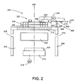
- FIG 2 shows a schematic cross sectional diagram of a plasma processing device like that shown in figure 1 but including an embodiment of an antenna arrangement according to present invention.
- the antenna arrangement includes inductive rf antenna 210 and a first passive antenna 220 and second passive antenna 222.
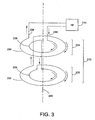
- Figure 3 shows a schematic circuit diagram illustrating the current path for the inductive antenna and
- figure 4 shows a schematic plan diagram illustrating the positioning of the passive antennae relative to the inductive antenna.
- Figure 2 shows the cross section along line AA' of figure 4 .
- the inductive antenna 210 comprises a first, upper pair 224 of circular antenna elements and a second, lower pair 226 of circular antenna elements.
- the upper pair comprises an inner loop antenna element 228 and an outer loop antenna element 230.
- the lower pair also comprises an inner loop antenna element 232 and an outer loop antenna element 234.
- the upper and lower pair are concentric about a central axis 245 extending substantially perpendicularly to the plane of the antenna.
- the central axis is co-linear with an axis of substantially cylindrical symmetry of the plasma chamber itself 202.
- Each antenna element is made of approximately 3/8" (0.9cm) square cross section silver plated copper.
- the inductive antenna has an inner diameter of approximately 6" (14.5cm) and an outer diameter of approximately 8" (19.4 cm).
- the antenna elements are mounted on a circular, cruciform cross section support 236 made of PTFE, available under the trade name Teflon. The dimensions of the support are sufficient to prevent arcing between the antenna elements.
- the support serves to hold the antenna elements in the correct relative spatial position and also helps to prevent the antenna elements from being repelled apart under magnetic forces during operation.
- the antenna elements are connected at their free ends to provide a single current path such that the current flows in the same sense within the plane of the antenna.
- rf current feeds 238 and 240 are provided at the free ends of the antenna 210 by which the rf power supply 214 supplies rf current to the antenna during operation.
- the rf current feeds are a source of azimuthal asymmetry in the predominantly symmetric electromagnetic field pattern that the antenna will generate. In general, not all rf antennae are designed to be azimuthally symmetric.
- the invention is not limited to the example rf antenna shown in the figures.
- the invention can be practiced using any rf inductive antenna configuration.
- alternative rf inductive antennae can have a single or multiple spiral antenna elements, wound as flat spirals or wound to lie on the surface of a hemisphere.
- an air gap between adjacent coils of the spiral can be used to prevent arcing between parts of the antenna.
- passive antenna 222 is mounted on a support 400.
- the support 400 includes an arm 402 which is journaled in a support body 404 which is pivotally mounted by a support foot 406 on the plasma chamber.
- the arm has a handle 408 at a first end and the passive antenna is attached at the other end.
- the support allows the position and orientation of the passive antenna to be adjusted with respect to the inductive antenna.
- the passive antenna can be translated 410 along the axis of the arm, rotated 412 about the axis of the arm, and the support body 404 can be rotated 414.
- the position of either or each passive antenna may be altered in any way as required.
- the passive antennae may be translated, rotated, tilted or otherwise oriented in three-dimensions with respect to the rf antenna.
- each of the passive antennae is held in place by a support structure connecting the passive antenna to a part of the plasma processing device.
- a support for the second passive antenna is not shown for the sake of clarity.
- the supports can serve to alter the position and orientation of the passive antennae, retain the passive antennae in a preferred position and also to prevent magnetic forces from moving the passive antennae.
- the passive antennae can be placed on ancillary parts of the plasma chamber, such as a window temperature controlling device, which provides a support for the antenna.
- Figure 4 shows a schematic plan view of the antenna arrangement of the present invention.
- the first passive antenna 220 and the second passive antenna 222 each has a 'D' shape and is made from an approximately 1" (2.4cm) wide band of silver plated copper.
- the passive antennae can be made of any electrically conducting material, but preferably are a metal and have as high a conductivity as possible. Taking the gap in the rf inductive antenna at the antenna feed point as 12 o'clock, the second passive antenna 222 is positioned at an angular position corresponding to approximately 1 o'clock and outside the periphery of the inductive antenna.
- the second passive antenna 220 is positioned at an angular position corresponding to approximately 7 o'clock and within the periphery of the inductive antenna. Both the passive antennae are positioned slightly above the upper surface of the inductive antenna, and within a plane substantially parallel to the plane of the inductive antenna.
- Figure 5 shows a contour plot 260 of the etch rate as a function of position over the surface of a wafer processed using a prior art plasma processing device similar to that shown in Figure 1 .
- the top center of the plot corresponds to the position of the RF antenna feed, and the center of the plot corresponds to the central axis 245 of the plasma processing device.
- the contour labels indicate the etch rate in units of Angstroms per minute. As can be seen, the etch rate is the highest in a sector toward the bottom left of the plot and the lowest in a sector toward the top right of the plot. Hence, there is a gradient in etch rate across the wafer.
- the etch rate is different in different directions around the wafer, therefore there is an azimuthal asymmetry in the etch rate over the wafer.
- the mean etch rate over the surface of the wafer is 29.9nm/min, with a standard deviation of 1.0nm/min and a range of 3.5nm/min.
- Figure 6 shows a contour plot 270 of the etch rate as a function of position over the surface of a wafer processed using the same process as that used in the process corresponding to figure 260, but using a plasma processing device having the antenna arrangement as shown in figures 2 and 4 .
- the top center of the plot corresponds to the position of the RF antenna feed, and the center of the plot corresponds to the central axis 245 of the plasma processing device.
- the contour labels indicate the etch rate in units of Angstroms per minute. As can be seen, the etch rate is the highest in a sector toward the left of the plot and the lowest in a sector toward the top right of the plot.
- the mean etch rate over the surface of the wafer is 29.7nm/min, which is comparable to the prior art process, but with a standard deviation of 0.5nm/min and a range of 1.8nm/min: i.e. the uniformity of the etch rate has been doubled and the variation in the etch rate with angle has been decreased. Therefore the etch rate using the antenna arrangement of the present invention has a greater uniformity and azimuthal symmetry than that of the prior art.
- a factor is believed to be the passive antennae modifying the rf field distribution in the plasma generating region to increase the azimuthal symmetry of the rf field distribution in the plasma generating region. Another factor would be important if the rf antenna and wafer are not co-axially aligned. In this case, no matter how symmetric the rf field distribution produced by the rf antenna alone, there would likely be significant variations in the etching rate over the wafer surface.
- the passive antennae are then used to modify the rf field distribution within the plasma chamber, and indeed may actually reduce the symmetry of the rf antenna rf field distribution within the plasma chamber, but actually increase the uniformity of the processing rate over the wafer surface, by generating an rf field distribution which increases the etch rate at areas of low etch rate, and vice versa, over the wafer surface.
- Figure 7 shows a schematic cross section of the rf antenna 210, first 220 and second 222 passive antennae, plasma generating region 252 and wafer 206 along line AA' of figure 4.
- Figure 7 also shows the instantaneous current and magnetic field distribution of the antenna arrangement.
- the rf current in the rf antenna is entering the right hand side of the rf antenna (passing into the page) and exiting the left hand side of the rf antenna (passing out of the page). This current results in the magnetic field pattern shown in solid lines.
- the first passive antenna 220 links magnetic flux of the rf antenna magnetic field and, according to Lenz's law, a current is induced in the passive antenna which generates a passive antenna magnetic field, shown in dashed lines, opposite in sense to the rf antenna magnetic field within the passive antenna. Hence the net magnetic field over the area of the passive antenna is reduced.
- the passive antenna magnetic field may be in the same direction as the rf antenna magnetic field in regions outside the area of the passive antenna so that the net magnetic field may be increased.
- the material of the passive antenna is not a perfect conductor, the magnetic field within the passive antenna is not perfectly cancelled out.
- the effect of the first passive antenna 220 is that the magnetic field at the position of the passive antenna within the rf antenna is reduced thereby also changing the rf field distribution within the processing chamber and over the plasma generating region 252. It should be understood that since the magnetic field from the rf antenna is an rf magnetic field, the magnetic field produced by the passive antenna is also an rf magnetic field.
- the second passive antenna 222 also links magnetic flux of the rf antenna magnetic field and, according to Lenz's law, a current is induced in the passive antenna 222 which generates a passive antenna rf magnetic field, shown in dashed lines, opposite in sense to the rf antenna magnetic field within the passive antenna. Hence the net magnetic field over the area of the passive antenna is reduced.
- the material of the passive antenna is not a perfect conductor, the magnetic field within the passive antenna is not perfectly cancelled out.
- the effect of the second passive antenna 220 is that the magnetic field at the position of the passive antenna outside the RF antenna is reduced thereby also changing the rf field distribution within the chamber and over the plasma generating region 252. As shown by figure 6 , the net effect of the two passive antennae is to increase the uniformity of the etch rate over the wafer surface.
- the passive antennae may be used to increase the symmetry (e.g. the azimuthal symmetry) of the rf field distribution in the plasma generating region.
- the passive antennae may be used to modify the rf field distribution in the processing chamber so as to reduce any inherent asymmetries in the rf antenna or the plasma processing device.
- the passive antennae may be used to reduce the symmetry of the rf antenna rf field distribution, if that results in a more uniform processing rate, e.g., because the wafer and rf antenna are misaligned.
- the passive antennae can be used to modify the rf field distribution within the plasma chamber to counteract any effects of elements of the plasma processing chamber on the electromagnetic field distribution, so as to improve the uniformity of plasma processing across the wafer.
- the passive antennae are inductively coupled to the rf antenna by linking the flux of the rf antenna magnetic field.
- the passive antennae do not require their own power supply.
- a one or all of the passive antennae can be placed in electrical contact with the rf antenna. However, even then the antennae are passive antennae as only induced rf currents will flow and not powered rf currents. The passive antennae would be maintained at the same voltage as the rf antenna.
- the present invention provides a way of fine tuning or trimming the rf electromagnetic field distribution within a plasma processing device by using appropriately placed and shaped passive antennae to modify the rf field distribution so as to increase the processing uniformity for a wafer.
- the passive antenna there are many possible ways of implementing the passive antenna which will depend on a number of factors, including the shape, size and nature of the modification to the rf field distribution that needs to be made, and more practical matters such as the space available within the plasma processing device in which the passive antenna can be placed.
- the location of the passive antenna relative to the rf antenna will also be a factor, as will the orientation of the passive antenna relative to the rf antenna.
- FIGS 8A-J show example alternative embodiments of the passive antenna.
- the passive antenna has the structure of an electrically conducting loop providing a low resistance current path so that a reasonable strength magnetic field will be induced by the RF antenna flux linked by the passive antenna.
- Figures 8A-G show perspective views of alternative passive antenna shapes.
- the passive antenna can have a curved shape, such as a circular shape, a segmental shape, a crescent shape, an oval or ellipsoidal shape.
- the passive antenna can also have a substantially polygonal shape, such as a square or triangular shape, and can be a regular or irregular polygon.
- the antenna can have an irregular shape, being made up of linear and curved sections or a combination of both.
- the passive antennae of figures 8A to G have a substantially flat planar shape.
- the passive antennae of figure 8H has a less planar, 'saddle' shape and the passive antenna of figure 8I also has non-flat planar shape.
- the passive antenna can be a more 3-dimensional body such as a sphere, spheroid, oblate spheroid, prolate spheroid, cube, and higher number of side bodies.
- the bodies can be regular or irregular and can have a solid surface or can have an aperture or apertures therein.
- FIG 9 shows an alternative embodiment of the antenna arrangement 300 of the present invention.
- the RF inductive antenna 210 is broadly the same as that described previously.
- a passive antenna 280 in the form of a circular band of silver plated copper and which is located co-axially of the RF antenna.
- the passive antenna is mounted on a support 500 so that the position of the passive antenna along the central axis 245 of the plasma processing device can be changed.
- the support includes an arm 502 which passes through an aperture in a support body 504 and so that the arm can slide along axis 245.
- a first end of the arm has a handle 506 and a second end of the arm has radially extending mounting elements 508 by which the passive antenna 280 is attached to the support.
- the mounting elements can be provided with azimuthal symmetry.
- the support can be non-electrically conducting and can be configured so as not to generate any further substantial electric or magnetic field asymmetries.
- the support maintains the passive antenna co-axial with the inductive antenna and the handle 506 of the support can be operated to change the position of the passive antenna along the axis 245.
- the magnetic field lines of the magnetic field generated by the RF antenna are shown for an instance in the rf cycle with the current distribution illustrated.
- the passive antenna links magnetic flux of the rf antenna magnetic field and, according to Lenz's law, a current is induced in the passive antenna 280 which generates a magnetic field (partially shown in broken lines) opposing the rf antenna field within the area of the passive antenna.
- a current is induced in the passive antenna 280 which generates a magnetic field (partially shown in broken lines) opposing the rf antenna field within the area of the passive antenna.
- the passive antenna magnetic field acts to increase the magnetic field outside the passive antenna. Therefore the magnetic field strength in the plasma region 252 around the periphery is increased.
- locating the circular passive antenna co-axial with the circular RF antenna modifies the radial distribution of the rf field distribution within the plasma chamber and in the plasma generating region 252.
- the radial rf field distribution can be altered within the plasma generating chamber so as to tune the magnetic field to optimize the plasma processing device for use with different etchants, e.g., argon and chlorine.
- Different diameter passive antenna will alter the radial distribution of the electromagnetic field in the plasma generating region. Also moving the passive loop along the central axis 245 will change the rf field distribution. Moving the passive coil away from the rf antenna and plasma region into position 282 (upward as shown in figure 9 ) will change the amount of rf antenna flux that is linked and will also reduce the contribution of the passive antenna field to the rf field distribution within the chamber. Moving the passive coil toward the plasma region 252 to position 284 will also change the RF flux linkage, but will decrease the distance between the passive antenna and chamber, thereby increasing the effect of the passive antenna field on the rf field distribution.
- the passive antenna 286 is outside the RF antenna and surrounds the RF antenna so as to change the radial distribution of the electromagnetic field at the plasma region.
- the antenna arrangement can include different types of rf antenna such as a spiral antenna or a hemispherical spiral antenna.
- the passive antenna can be located non-coaxially with the rf antenna and may or may not be the same shape as the rf antenna. In the example embodiment shown in figure 9 , moving the passive antenna along the rf antenna axis means that it is substantially the radial component of the rf field distribution that is modified.
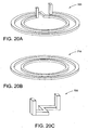
- FIG 10 shows a schematic perspective drawing of a further embodiment 320 of the antenna arrangement of the invention.
- the passive antenna 330 is provided in the form of a shield which encloses the rf antenna 210 and extends along most of the length of the rf antenna, apart from the rf feed part of the rf antenna.
- the passive antenna also encloses the rf feed part of the rf antenna. This can be beneficial if the rf feed part of the antenna is a major source of the asymmetry in the rf antenna rf field.
- the passive antenna 330 has a substantially annular shape.
- the passive antenna is made from an appropriately shaped sheet of silver plated copper.
- At least one gap in the passive antenna should be provided, because a shield passive antenna that enclosed the rf antenna along the whole of its length would completely contain rf magnetic field of the antenna, not allowing the rf magnetic field to reach to the plasma generating region.
- the cross-sectional shape of the passive antenna is the same as the shape of the magnetic field lines of the magnetic field that the rf antenna would generate in the absence of any asymmetries.
- the surface of the passive antenna is such that it is parallel to the desired symmetric parts of the rf antenna field.
- the embodiment 320 of the passive antenna shown in figure 10 is beneficial in providing maximal screening of some of the asymmetries in the rf antenna field within the constraints of requiring a feed position and a gap to allow the RF antenna magnetic field out.
- the passive antenna 330 also acts as a Faraday shield to an extent.
- the part of the surface of the passive antenna located between the rf antenna and window provides a substantially annular Faraday shield and reduces the capacitive coupling between the rf antenna and the plasma (although there will still be a capacitive component of the rf field distribution within the plasma chamber).
- the shielding passive antenna 330 is configured so as to modify the rf field distribution by removing the undesired asymmetric parts from the inductive field.
- conventional Faraday shields are configured so as to pass the inductive part of the rf field without modifying it.
- FIG 11 shows a schematic perspective drawing of a further embodiment 340 of the antenna arrangement of the invention.
- the passive antenna 350 is provided in the form of a shield which encloses the rf antenna 210 about a part diametric to the feed part of the rf antenna.
- the passive antenna is made of an appropriately formed sheet of silver plated copper.
- the passive antenna again has a cross sectional shape which is parallel to the magnetic field lines of the symmetric parts of the rf antenna field so as to shield out the asymmetric parts.
- the passive shielding antenna can be located at a position about the rf antenna diametrically opposite the feed part.
- Figures 12A to 12C show cross sectional drawings of the RF antenna 210.
- Figure 12A shows a magnetic field line 342 at an instance of the RF cycle for the perfectly symmetric RF antenna.
- Figure 12B shows a magnetic field line 344 at an instance of the RF cycle for an asymmetric RF antenna, in which a lobe 346 representing the asymmetric part of the field pattern has been added to the perfect field pattern shown in Figure 12A.
- Figure 12C shows a shielding passive antenna 360 having the same cross sectional shape as the symmetric RF antenna field pattern. The surface of the passive antenna is parallel to the magnetic field line 344 of the magnetic field at every position except the lobe part.
- Every part of the magnetic field in the lobe part 362 can be decomposed into a component which is parallel 364 to the symmetric field line 342 and a component that is perpendicular 366 to the symmetric field line 342.
- the passive antenna surface is parallel to the symmetric field, it will be at all places parallel to the component parallel to the symmetric field and at all places present a surface normal to any perpendicular component.
- the perpendicular component will, according to Lenz's law, induce a surface current 370 in the passive antenna, which generates a magnetic field 372 to cancel the perpendicular component.
- the passive antenna 360 inductively couples with the magnetic field of the rf antenna and surface currents are induced which cancel the non-symmetric part of the rf antenna field at everywhere on the surface of the passive antenna.
- the symmetry of the rf antenna field is increased thereby increasing the symmetry of the electromagnetic field in the plasma generating region.
- FIGs 14 to 17 show alternate embodiments of the shielding inductively coupled passive antenna.
- the passive antenna 380 shown in figure 14 is in the form of a substantially circular, annular plate, made of silver plated copper having a first gap 381 and a second gap 383.
- the width of the annular part of the plate is less than the radius of the inner diameter of the annular plate.
- Two gaps increase the efficacy of the Farday shielding aspect of the passive antenna. Two gaps reduces the potential difference between adjacent ends of the annular shield, compared to the case of a single gap. More than two gaps can be used.
- the shape of the passive antenna is configured so as to modify the inductive part of the rf field distribution by allowing surface currents to be induced to remove unwanted asymmetric parts of the rf antenna field.
- the passive antenna In use such a shielding antenna would be located concentric with and above or below the RF antenna.
- the passive antenna will provide no Faraday shielding effect when not disposed at least partially between the rf antenna and plasma. This passive antenna can shield out those asymmetric components of the RF antenna magnetic field perpendicular to its surface.
- the passive antenna 380 can be distinguished as being configured so as to produce a current path allowing surface currents to be induced in its surface so as to cancel out undesired inductive parts of the rf antenna field.
- a Faraday shield is configured specifically to pass the inductive part of the rf field unchanged.
- Figure 15 shows a passive antenna 382 in the form of an annular, three-sided rectangular trough so as to shield out those unwanted inductive parts of the rf antenna field from the sides and below.
- a curved trough e.g., U or C shaped in cross section could also be used, as appropriate and depending in the shape of the RF antenna magnetic field pattern that it is necessary to match.
- more than one gap can be provided in the passive antenna to improve its Faraday shielding performance.
- Other embodiments of the shielding passive antenna can include an inner wall, an outer wall, a top wall or a side wall of the shield, or any combination thereof, with as many gaps as are appropriate for the application.
- FIG 16 shows a further alternative embodiment 384 of the antenna arrangement.
- the rf inductive antenna 386 is shown as a simple wire loop having an rf feed point 388.
- the wire loop would have a poloidal magnetic field pattern.
- the passive antenna 390 is provided in the form of six metal, curved cylinder-like sections, each enclosing a section of the rf antenna.
- the sections each have a respective radially extending metal limb 391 by which they are connected at a central hub 392. This improves the Faraday shielding effect of the passive antenna 390.
- Each of the sections has approximately the same length and the spacing between sections is approximately the same.
- each section and gap extends over an angle of approximately 30°, and the sections are equi-angularly regularly spaced about the rf antenna.
- the passive antenna is made to be as azimuthally symmetric as possible, thereby helping to reduce introduction of any azimuthal asymmetries by the passive antenna.
- providing the passive antenna along substantially the whole of the length of the RF antenna helps to reduce large scale asymmetries in the azimuthal symmetry in the plasma region, while small scale diffusion of the plasma helps to increase the overall azimuthal symmetry of the plasma itself.
- the fine scale positioning of the sections may not be perfectly azimuthally symmetric so as to help counteract the effect of the location of the antenna feed. Further, in another embodiment there may be an odd number of sections such that a section, rather than a gap, is diametrically opposed to the location of the feed.
- Each of the sections of the shielding passive antenna 390 acts as a perturbation on the magnetic field that the rf antenna generates.
- the perturbing effect of the shielding antenna sections can be reduced by making the cross sectional shape of the edges of the ends of each section the same as the magnetic field lines of the rf antenna magnetic field would have at the gap regions between the sections in the absence of the passive antenna.
- the natural, symmetric magnetic field for the circular rf antenna, in the absence of the shielding antenna 390 would be a poloidal field having a circular cross section in the plane perpendicular to the wire of the wire loop rf antenna 386. Therefore, the perturbing effect of the shielding antenna sections can be reduced by making the cross sectional shape of the edge 387, of each end part 389 of the sections circular also. This helps to smooth the transition between the shielding sections and the gaps in the passive antenna.
- the cross section of the passive antenna sections in figure 16 is shown as the same along the length of each section, it can be appropriate for the cross sectional shape of the passive antenna to vary along its length along the rf antenna.
- making the cross sectional shape of the edges of the ends of the passive antenna the same as the magnetic field lines that the rf antenna magnetic field would have in the absence of the passive antenna can help to reduce the perturbing effect of the passive antenna on the rf field distribution.
- FIG 17 shows the simplest embodiment of the shielding passive antenna 392.
- the passive antenna is provided in the form of a substantially planar, rectangular sheet of silver plated copper.
- the sheet provides a surface current path 394, so that when the sheet is located adjacent the rf antenna, it can inductively couple to the rf antenna field, and a canceling field will be generated to reduce an asymmetric part of the rf antenna field and modify the rf field distribution in the plasma chamber in such a way as to increase the processing uniformity.
- FIG 18 shows a schematic cross sectional view of a plasma processing apparatus 500 similar to that shown in figure 2 , and having an additional electromagnet arrangement 510
- the electromagnet arrangement includes a first outer circular coil 514 and a second inner circular coil 516 concentric to the plasma chamber. Each coil is connected to a variable supply of DC electrical power 520 which supplies a DC current to each coil and which flows in opposite directions in each coil.
- Plasma processing apparatus 500 also includes a magnetic bucket arrangement 522, which includes a plurality of permanent magnets axially oriented around the periphery of the plasma processing chamber. The magnetic bucket arrangement is configured to provide a permanent DC magnetic field which keeps the plasma current density gradient away from the wafer 206 while simultaneously maintaining a very small magnetic field at the wafer 206.
- the magnetic bucket arrangement helps to reduce plasma loss to the wall of the plasma processing chamber.
- the magnetic bucket arrangement includes thirty two permanent magnet cusps that have their radial magnetization factors alternating around the chamber (e.g., N, S, N, S etc.). However, the actual number of cusps may vary according to the specific design of each plasma processing system.
- the electromagnetic coil arrangement is configured to provide a DC magnetic field having a controllable radial variation within the plasma processing chamber in the region proximate the window 212.
- the radial variation in the DC magnetic field is made by varying at least one of the DC currents flowing in at least one of the coils.
- the radial variation in the DC magnetic field is effective to affect the processing uniformity across the wafer 206.
- the DC magnetic field can be constant or can be allowed to vary slowly with time, if required to match variations in processing.
- the DC magnetic field distribution provided by the coil arrangement and bucket arrangement, together or separately, helps to prevent lateral diffusion of the plasma species and so helps to both confine the plasma and also collimate the plasma species, so as to enhance their transport toward the wafer surface. In the absence of the DC field, lateral plasma diffusion tends to wash out or reduce asymmetries in the plasma generating region by time the plasma reaches the wafer. As the DC magnetic field helps to retain the plasma species at the wafer surface in a similar configuration to that of the plasma, any non-uniformities in the plasma distribution will be more evident at the wafer surface.
- any asymmetries in the plasma distribution is enhanced at the wafer surface by the use of a DC magnetic field provided by the DC electromagnets arrangement 510 or the bucket arrangement 522 or both.
- the passive antennae asymmetries in the plasma distribution can be reduced, such that the benefits of using the DC magnetic field to increase the transport of plasma species to the wafer surface can be realized without significantly reducing the etching uniformity.
- the benefit from eliminating the asymmetries using passive antennae can be larger when the DC magnetic fields are present.
- lateral plasma species diffusion can increase the uniformity of etching on the wafer surface.
- the reduction of lateral diffusion by the DC magnetic fields means that the improved uniformity of the plasma caused by the passive antenna is more usefully propagated to the wafer surface to provide uniform etching.
- the use of a constant or slowly time varying DC magnetic fields provided by the permanent bucket magnets and/or electromagnet arrangement enhances the effect of the passive antennae on the uniformity of etching that can be achieved.
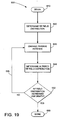
- Figure 19 shows a flow chart 600 illustrating a method for tuning the rf field distribution that is provided in a plasma chamber.
- the first step is to determine 620 the rf field distribution that results from the rf antenna.
- a passive antenna is added 630 to the rf antenna and inductively coupled to the rf antenna.
- the altered rf field distribution arising as a result of the interaction between the passive antenna and the rf antenna is determined. If the resulting rf field distribution is determined 650 by a criterion to result in an increased processing uniformity, then the method can terminate at step 600.
- a passive antenna can be 'added' 630 by either adding further passive antenna or antennae, or the original passive antenna can be replaced by a different passive antenna, or the original passive antenna can be reconfigured, for example, by repositioning it with respect to the rf antenna.
- the new altered rf field distribution is then re-determined 640 and the increase in processing uniformity re-determined 650.
- the steps of adding passive antennae and re-determining the rf field distribution can be iterated as many times as are required until a selected processing uniformity metric or threshold has been achieved.
- the tuning method can be computational and can be directed at increasing the symmetry of the rf field generated by the rf antenna and passive antenna, or antennae, at the plasma generating region in the plasma chamber or otherwise to alter the rf field distribution in the plasma processing device so as to increase the processing uniformity.
- the determination of the rf field distribution can be carried out using a computer and suitable electromagnetic field modeling software. An example of a commercially available software package would be Maxwell 3d as provided by Ansoft Corp. Given the shape of the rf antenna and certain boundary conditions the various components of the vector rf field in space around the antenna can be calculated. The shape of the antenna can be varied and various passive antennae can be added into the calculation so as to optimize to obtain the most uniform resulting rf fields for certain restrictions, such as a minimal antenna part separation to prevent arcing.
- an actual rf antenna 700 can be conceptualized as perfectly symmetric rf antenna 710 and a perturbing part 720 representing the rf antenna feeds and cross over parts.
- the objective is to provide a passive antenna which reduces the contribution of the perturbing part 720 to the rf field distribution while minimizing effect of the passive antenna on the rf field distribution provided by the symmetric part 710.
- the ideal solution would be a passive antenna with the same shape as part 720 and with an equal and opposite phase rf current flowing in it. However, the passive antenna cannot occupy the same physical space as the physical feed and cross over parts. Initially the rf field distribution is calculated 620 for the powered rf antenna alone, taking into account the rf feeds, any missing segments and other sources of asymmetry, and in the absence of any passive antennae.
- one or more passive antennae are introduced 630 and the rf field distribution is calculated again 640 and the affect on processing uniformity assessed 650.
- Different passive antennae configurations can be provided and the rf field distributions re-calculated 635, until a preferred passive antenna or antennae configuration is arrived at which gives the most symmetric calculated rf field distribution, or the rf field distribution otherwise providing increased processing uniformity, e.g. if it is known that there is a particular source of processing non-uniformity in the plasma processing device that the rf field distribution is to be changed to correct for.
- the computationally derived passive antennae can then be realized and implemented.
- the rf field distribution of an rf antenna and rf antenna and passive antenna configuration is measured using an electromagnetic field measuring device.
- the rf antenna is placed in an etch chamber or put in an rf test stand and powered using a low voltage signal.
- the vector rf field distribution in space around the rf antenna, in the absence of any passive antennae, is measured using an rf pick-up probe to determine 620 the rf field distribution.
- a suitable rf pick-up probe can comprise a short section of rigid coaxial conductor bent into a single loop and with the inner conductor shorted to the outer conductor.
- One or more passive antennae are added 630 to the rf antenna and the resulting rf field distribution is again measured using an rf probe to determine the altered rf field distribution 640. It is determined 650 if the measured rf field distribution meets a processing uniformity criterion or criteria, such as a particular degree of symmetry, and if not 635 then other passive antenna configurations are assembled and their rf field distributions measured. Passive antenna numbers, positions, orientations, shapes and other properties affecting the rf field they generate may be varied in order to provide an optimized processing uniformity. When a suitable rf antenna and passive antenna configuration has been derived, the rf antenna and passive antenna can be installed in a plasma etching device and their relative positions fixed so that further measurements or testing can be carried out or plasma processing can be carried out directly.
- work piece processing is used to help determine the rf field distributions.
- a wafer is used as a work piece and is located in a plasma processing tool.
- An etch is carried out using an rf antenna and no passive antennae, and the process uniformity across the wafer is measured and quantified, for example by measuring the etch rate over the surface of a wafer.
- the etch uniformity is related to the rf field distribution within the plasma chamber and so a measure of the rf field distribution is determined by this step 620.
- a passive antenna is then added to the rf antenna 630 and another work piece wafer is etched under the otherwise identical processing conditions and the processed wafer is measured and degree of etching over the wafer surface quantified.
- the difference between the rf antenna alone and the rf antenna and passive antenna processing is then obtained to give a measure of the effect of the passive antenna on the etching uniformity.
- a passive antenna at a first angular position of the rf antenna may increase the etch rate at the corresponding angular position on the wafer.
- the passive antenna can then be replaced by a differently shaped or sized passive antenna, or the position or orientation of the passive antenna varied or further passive antennae can be added 630 and then another etch carried out on a new wafer to determine 640 the processing uniformity for that configuration.
- the correction required to provide optimal uniformity can be determined from the difference between the rf antenna alone etching pattern and an entirely uniform etching pattern.
- the combination of passive antennae and rf antenna sufficiently closely matching that difference will provide the optimal uniformity based on the antenna configurations measured so far. If generic relationships are identified, such as increases in passive antenna size or distance from the rf antenna having reasonably fixed relationships to their effect on the processing rate, then reasonably accurate estimates as to the appropriate passive antenna size and position can be made based on the measured results. For example doubling the area enclosed by a passive antenna may increase the change in etch rate at the wafer in a predictable manner.
- the tool When it is determined that the rf antenna and passive antennae configuration provides processing uniformity, within an acceptable range, then the tool has been tuned for work piece processing proper and the method ends 660. Alternatively further iterations and fine tuning can be carried out using the thus far optimized rf antenna and passive antennae configuration.
- Tuning the rf field distribution using this later method is believed to be particularly useful as it is believed that after major sources of non-uniformity have been removed, the sources of processing non-uniformity in otherwise identical processing tools vary substantially randomly from tool to tool. Therefore fine tuning of each processing tool on a tool by tool basis to achieve increased processing uniformity can be carried out to determine the rf antenna and passive antenna configuration that is optimal for each tool.
Claims (16)
- Une disposition d'antenne pour générer une distribution de champ rf dans une zone de production de plasma à l'intérieur d'une paroi de chambre d'une chambre de traitement (202) d'un appareil de traitement du plasma, comprenant :Une antenne inductive rf (210) à laquelle une alimentation électrique rf (214) est connectée pour fournir un courant rf pour générer un premier champ rf s'étendant dans la zone de production de plasma ; etUne antenne passive (220), l'antenne passive étant raccordée de façon inductive à l'antenne inductive rf (210) et configurée pour générer un deuxième champ rf modifiant le premier champ rf de sorte que la distribution radiale et azimutale de la distribution de champ rf dans la zone de production de plasma altère et par conséquent augmente l'uniformité de traitement de l'appareil de traitement comparé à celui en l'absence d'antenne passive (220), où le deuxième champ rf modifie le premier champ rf de sorte que la distribution du champ rf dans la zone de production de plasma possède une symétrie différente de celle en l'absence de l'antenne passive (220) ; où l'antenne passive (220) fournit une voie électriquement conductrice sur laquelle un courant électrique induit passe pour générer au moins une partie du deuxième champ rf.
- La disposition de l'antenne de la revendication 1, où l'antenne passive (220) change la symétrie azimutale de la distribution du champ rf dans la région de production de plasma.
- La disposition de l'antenne de la revendication 2, où la symétrie azimutale de la distribution de champ rf est augmentée par rapport à celle en l'absence de l'antenne passive.
- La disposition de l'antenne de la revendication 1, et incluant une pluralité d'antennes passives (220, 222), chaque antenne inductivement raccordée à l'antenne inductive rf et configurée pour générer un champ rf respectif modifiant de plus le premier champ rf de sorte que la distribution de champ rf dans la zone de production de plasma augmente l'uniformité de traitement de l'appareil de traitement comparée à celle en l'absence des antennes passives.
- La disposition de l'antenne de la revendication 1, où l'antenne passive s'étend le long d'au moins une partie de la longueur de l'antenne inductive.
- La disposition de l'antenne de la revendication 1, où l'antenne passive possède une forme de canal qui s'étend au moins partiellement autour d'une partie de l'antenne inductive.
- La disposition de l'antenne de la revendication 1, où l'antenne passive comprend une partie de l'antenne inductive.
- La disposition de l'antenne de la revendication 7, où l'antenne passive comprend l'antenne inductive le long principalement de toute la longueur de l'antenne inductive.
- La disposition de l'antenne de la revendication 1, où l'antenne passive possède une forme transversale correspondant principalement à la forme des lignes de champ magnétique que le premier champ rf aurait à l'endroit de l'antenne passive en l'absence de toute imperfection dans la symétrie du premier champ rf.
- La disposition de l'antenne de la revendication 1, où l'antenne passive possède une région finale avec un bord et le bord de la région finale de l'antenne passive possède une forme transversale correspondant principalement à la forme des lignes de champ magnétique que le premier champ rf aurait à l'endroit du bord de la région finale de l'antenne passive en l'absence de l'antenne passive.
- La disposition de l'antenne de la revendication 7, comprenant de plus une pluralité d'antennes passives où l'antenne passive et une pluralité d'antennes passives sont disposées de façon angulaire autour de l'antenne inductive rf.
- La disposition de l'antenne de la revendication 11, où l'antenne passive et la pluralité des antennes passives sont principalement disposées de façon équi-angulaire autour de l'antenne inductive.
- La disposition de l'antenne de la revendication 1, comprenant de plus :Une disposition d'un électroaimant (522) qui génère un champ magnétique CC dans la chambre de traitement.
- Une méthode pour améliorer l'uniformité de traitement de plasma dans le dispositif de traitement de plasma de la revendication 1, comprenant les étapes de :Connexion de l'antenne inductive rf (210) à l'alimentation électrique rf (214) pour fournir un courant rf pour générer un premier champ rf s'étendant dans la zone de production de plasma ;Raccord inductif de l'antenne passive (220) et de l'antenne inductive rf (210), etPositionnement de l'antenne passive (220) pour faire en sorte que le deuxième champ rf modifie le premier champ rf de sorte que la distribution radiale et azimutale de la distribution du champ rf dans la zone de production de plasma altère et par conséquent augmente l'uniformité de traitement de l'appareil de traitement comparée à celle en l'absence de l'antenne passive (220) ; etL'application d'un champ magnétique CC à la chambre de traitement (202).
- La méthode de la revendication 14, où le champ magnétique CC est appliqué par un électroaimant et le champ magnétique CC possède une variation radiale qui est effective pour affecter l'uniformité de traitement du plasma.
- La méthode de la revendication 14, où le champ magnétique CC est appliqué par un dispositif magnétique à aimant permanent.
Applications Claiming Priority (3)
| Application Number | Priority Date | Filing Date | Title |
|---|---|---|---|
| US200833 | 2002-07-22 | ||
| US10/200,833 US6842147B2 (en) | 2002-07-22 | 2002-07-22 | Method and apparatus for producing uniform processing rates |
| PCT/US2003/022206 WO2004010457A1 (fr) | 2002-07-22 | 2003-07-17 | Procede et appareil pour produire des vitesses de traitement uniformes |
Publications (2)
| Publication Number | Publication Date |
|---|---|
| EP1540694A1 EP1540694A1 (fr) | 2005-06-15 |
| EP1540694B1 true EP1540694B1 (fr) | 2015-11-11 |
Family
ID=30769568
Family Applications (1)
| Application Number | Title | Priority Date | Filing Date |
|---|---|---|---|
| EP03765610.5A Expired - Lifetime EP1540694B1 (fr) | 2002-07-22 | 2003-07-17 | Procede et appareil pour produire des taux de traitement uniformes |
Country Status (9)
| Country | Link |
|---|---|
| US (1) | US6842147B2 (fr) |
| EP (1) | EP1540694B1 (fr) |
| JP (2) | JP4928077B2 (fr) |
| KR (1) | KR100974844B1 (fr) |
| CN (3) | CN102573265B (fr) |
| AU (1) | AU2003256565A1 (fr) |
| IL (1) | IL166342A (fr) |
| TW (1) | TWI327875B (fr) |
| WO (1) | WO2004010457A1 (fr) |
Families Citing this family (32)
| Publication number | Priority date | Publication date | Assignee | Title |
|---|---|---|---|---|
| KR200253559Y1 (ko) * | 2001-07-30 | 2001-11-22 | 주식회사 플라즈마트 | 회전방향으로 균일한 플라즈마 밀도를 발생시키는유도결합형 플라즈마 발생장치의 안테나구조 |
| JP2003323997A (ja) * | 2002-04-30 | 2003-11-14 | Lam Research Kk | プラズマ安定化方法およびプラズマ装置 |
| KR100486724B1 (ko) * | 2002-10-15 | 2005-05-03 | 삼성전자주식회사 | 사행 코일 안테나를 구비한 유도결합 플라즈마 발생장치 |
| US20050205211A1 (en) * | 2004-03-22 | 2005-09-22 | Vikram Singh | Plasma immersion ion implantion apparatus and method |
| KR100968132B1 (ko) * | 2008-02-29 | 2010-07-06 | (주)얼라이드 테크 파인더즈 | 안테나 및 이를 구비한 반도체 장치 |
| US8298949B2 (en) | 2009-01-07 | 2012-10-30 | Lam Research Corporation | Profile and CD uniformity control by plasma oxidation treatment |
| EP2396804B1 (fr) * | 2009-02-10 | 2014-03-26 | HELYSSEN S.à.r.l. | Appareil pour traitement au plasma d'une zone étendue |
| US9337004B2 (en) * | 2009-04-06 | 2016-05-10 | Lam Research Corporation | Grounded confinement ring having large surface area |
| KR101757921B1 (ko) * | 2009-10-27 | 2017-07-14 | 도쿄엘렉트론가부시키가이샤 | 플라즈마 처리 장치 및 플라즈마 처리 방법 |
| JP5694721B2 (ja) * | 2009-10-27 | 2015-04-01 | 東京エレクトロン株式会社 | プラズマ処理装置及びプラズマ処理方法 |
| US8741097B2 (en) * | 2009-10-27 | 2014-06-03 | Tokyo Electron Limited | Plasma processing apparatus and plasma processing method |
| US9313872B2 (en) * | 2009-10-27 | 2016-04-12 | Tokyo Electron Limited | Plasma processing apparatus and plasma processing method |
| JP5592098B2 (ja) * | 2009-10-27 | 2014-09-17 | 東京エレクトロン株式会社 | プラズマ処理装置及びプラズマ処理方法 |
| JP5451324B2 (ja) * | 2009-11-10 | 2014-03-26 | 株式会社日立ハイテクノロジーズ | プラズマ処理装置 |
| JP5723130B2 (ja) * | 2010-09-28 | 2015-05-27 | 東京エレクトロン株式会社 | プラズマ処理装置 |
| JP5916044B2 (ja) * | 2010-09-28 | 2016-05-11 | 東京エレクトロン株式会社 | プラズマ処理装置及びプラズマ処理方法 |
| JP5639866B2 (ja) * | 2010-12-03 | 2014-12-10 | 株式会社日立ハイテクノロジーズ | プラズマ処理装置 |
| JP5781349B2 (ja) * | 2011-03-30 | 2015-09-24 | 東京エレクトロン株式会社 | プラズマ処理装置 |
| US10271416B2 (en) * | 2011-10-28 | 2019-04-23 | Applied Materials, Inc. | High efficiency triple-coil inductively coupled plasma source with phase control |
| US20130256271A1 (en) * | 2012-04-03 | 2013-10-03 | Theodoros Panagopoulos | Methods and apparatuses for controlling plasma in a plasma processing chamber |
| JP6248562B2 (ja) * | 2013-11-14 | 2017-12-20 | 東京エレクトロン株式会社 | プラズマ処理装置及びプラズマ処理方法 |
| CN104684235B (zh) * | 2013-11-28 | 2017-07-07 | 中微半导体设备(上海)有限公司 | 一种电感线圈组及电感耦合等离子体处理装置 |
| CN105719928A (zh) * | 2014-12-03 | 2016-06-29 | 中微半导体设备(上海)有限公司 | Icp刻蚀中对刻蚀速率非均匀性进行补偿的装置和方法 |
| JP6603999B2 (ja) * | 2015-02-13 | 2019-11-13 | 日新電機株式会社 | プラズマ処理装置 |
| US10297457B2 (en) | 2015-03-19 | 2019-05-21 | Mattson Technology, Inc. | Controlling azimuthal uniformity of etch process in plasma processing chamber |
| JP6053881B2 (ja) * | 2015-07-15 | 2016-12-27 | 東京エレクトロン株式会社 | プラズマ処理装置 |
| US10128083B2 (en) * | 2016-06-01 | 2018-11-13 | Vebco Instruments Inc. | Ion sources and methods for generating ion beams with controllable ion current density distributions over large treatment areas |
| US9899193B1 (en) * | 2016-11-02 | 2018-02-20 | Varian Semiconductor Equipment Associates, Inc. | RF ion source with dynamic volume control |
| CN108271309B (zh) * | 2016-12-30 | 2020-05-01 | 中微半导体设备(上海)股份有限公司 | 一种电感耦合等离子处理装置 |
| US11280861B2 (en) * | 2018-06-17 | 2022-03-22 | Skope Magnetic Resonance Technologies Ag | Sheath wave barrier for magnetic resonance (MR) applications |
| US11078570B2 (en) * | 2018-06-29 | 2021-08-03 | Lam Research Corporation | Azimuthal critical dimension non-uniformity for double patterning process |
| CN114599142A (zh) * | 2022-03-07 | 2022-06-07 | 盛吉盛(宁波)半导体科技有限公司 | 等离子体调节装置、方法、生成装置和半导体加工装置 |
Family Cites Families (13)
| Publication number | Priority date | Publication date | Assignee | Title |
|---|---|---|---|---|
| US5401350A (en) * | 1993-03-08 | 1995-03-28 | Lsi Logic Corporation | Coil configurations for improved uniformity in inductively coupled plasma systems |
| US5731565A (en) * | 1995-07-27 | 1998-03-24 | Lam Research Corporation | Segmented coil for generating plasma in plasma processing equipment |
| US5907221A (en) * | 1995-08-16 | 1999-05-25 | Applied Materials, Inc. | Inductively coupled plasma reactor with an inductive coil antenna having independent loops |
| US5759280A (en) * | 1996-06-10 | 1998-06-02 | Lam Research Corporation | Inductively coupled source for deriving substantially uniform plasma flux |
| US5897712A (en) * | 1996-07-16 | 1999-04-27 | Applied Materials, Inc. | Plasma uniformity control for an inductive plasma source |
| WO1998042012A1 (fr) * | 1997-03-17 | 1998-09-24 | Matsushita Electric Industrial Co., Ltd. | Procede et dispositif permettant le traitement de plasma |
| US6237526B1 (en) * | 1999-03-26 | 2001-05-29 | Tokyo Electron Limited | Process apparatus and method for improving plasma distribution and performance in an inductively coupled plasma |
| US6310577B1 (en) * | 1999-08-24 | 2001-10-30 | Bethel Material Research | Plasma processing system with a new inductive antenna and hybrid coupling of electronagnetic power |
| US6320320B1 (en) * | 1999-11-15 | 2001-11-20 | Lam Research Corporation | Method and apparatus for producing uniform process rates |
| US6341574B1 (en) * | 1999-11-15 | 2002-01-29 | Lam Research Corporation | Plasma processing systems |
| US6508198B1 (en) * | 2000-05-11 | 2003-01-21 | Applied Materials Inc. | Automatic tuning in a tapped RF transformer inductive source of a plasma reactor for processing a semiconductor wafer |
| US6414648B1 (en) * | 2000-07-06 | 2002-07-02 | Applied Materials, Inc. | Plasma reactor having a symmetric parallel conductor coil antenna |
| JP2003234338A (ja) * | 2002-02-08 | 2003-08-22 | Tokyo Electron Ltd | 誘導結合プラズマ処理装置 |
-
2002
- 2002-07-22 US US10/200,833 patent/US6842147B2/en not_active Expired - Lifetime
-
2003
- 2003-07-17 KR KR1020057001224A patent/KR100974844B1/ko active IP Right Grant
- 2003-07-17 CN CN201110437893.2A patent/CN102573265B/zh not_active Expired - Lifetime
- 2003-07-17 CN CN200810178065XA patent/CN101460002B/zh not_active Expired - Lifetime
- 2003-07-17 AU AU2003256565A patent/AU2003256565A1/en not_active Abandoned
- 2003-07-17 EP EP03765610.5A patent/EP1540694B1/fr not_active Expired - Lifetime
- 2003-07-17 JP JP2004523453A patent/JP4928077B2/ja not_active Expired - Lifetime
- 2003-07-17 CN CN038225794A patent/CN1689132B/zh not_active Expired - Lifetime
- 2003-07-17 WO PCT/US2003/022206 patent/WO2004010457A1/fr active Application Filing
- 2003-07-22 TW TW092120008A patent/TWI327875B/zh active
-
2005
- 2005-01-17 IL IL166342A patent/IL166342A/en not_active IP Right Cessation
-
2011
- 2011-12-21 JP JP2011279987A patent/JP2012104496A/ja not_active Withdrawn
Also Published As
| Publication number | Publication date |
|---|---|
| JP2012104496A (ja) | 2012-05-31 |
| IL166342A (en) | 2009-08-03 |
| CN102573265A (zh) | 2012-07-11 |
| TW200405768A (en) | 2004-04-01 |
| AU2003256565A1 (en) | 2004-02-09 |
| JP2005534150A (ja) | 2005-11-10 |
| IL166342A0 (en) | 2006-01-16 |
| EP1540694A1 (fr) | 2005-06-15 |
| WO2004010457A1 (fr) | 2004-01-29 |
| KR20050025975A (ko) | 2005-03-14 |
| US6842147B2 (en) | 2005-01-11 |
| CN102573265B (zh) | 2016-01-20 |
| TWI327875B (en) | 2010-07-21 |
| JP4928077B2 (ja) | 2012-05-09 |
| CN101460002B (zh) | 2012-07-04 |
| CN1689132B (zh) | 2010-06-16 |
| CN1689132A (zh) | 2005-10-26 |
| CN101460002A (zh) | 2009-06-17 |
| KR100974844B1 (ko) | 2010-08-11 |
| US20040085246A1 (en) | 2004-05-06 |
Similar Documents
| Publication | Publication Date | Title |
|---|---|---|
| EP1540694B1 (fr) | Procede et appareil pour produire des taux de traitement uniformes | |
| KR100712762B1 (ko) | 유도 결합 플라스마에서 플라스마 분포 및 성능을 개선하는 처리 장치 및 방법 | |
| KR100590344B1 (ko) | 유도 결합 플라즈마에서 플라즈마 분포 및 성능을향상시키는 장치 및 방법 | |
| US6806437B2 (en) | Inductively coupled plasma generating apparatus incorporating double-layered coil antenna | |
| KR100551138B1 (ko) | 균일한 플라즈마 발생을 위한 적응형 플라즈마 소스 | |
| KR100238627B1 (ko) | 플라즈마 처리장치 | |
| TWI467624B (zh) | Plasma processing device and plasma processing method | |
| KR101091356B1 (ko) | 대규모 유도 결합 플라즈마 소스용 유도 소자 | |
| JP3903034B2 (ja) | 蛇行コイルアンテナを具備した誘導結合プラズマ発生装置 | |
| KR102031198B1 (ko) | 플라즈마 처리 장치 및 플라즈마 처리 방법 | |
| EP1305453A1 (fr) | Source de plasma annulaire a densite elevee et procede associe |
Legal Events
| Date | Code | Title | Description |
|---|---|---|---|
| PUAI | Public reference made under article 153(3) epc to a published international application that has entered the european phase |
Free format text: ORIGINAL CODE: 0009012 |
|
| 17P | Request for examination filed |
Effective date: 20050114 |
|
| AK | Designated contracting states |
Kind code of ref document: A1 Designated state(s): AT BE BG CH CY CZ DE DK EE ES FI FR GB GR HU IE IT LI LU MC NL PT RO SE SI SK TR |
|
| AX | Request for extension of the european patent |
Extension state: AL LT LV MK |
|
| DAX | Request for extension of the european patent (deleted) | ||
| 17Q | First examination report despatched |
Effective date: 20100212 |
|
| REG | Reference to a national code |
Ref country code: DE Ref legal event code: R079 Ref document number: 60348248 Country of ref document: DE Free format text: PREVIOUS MAIN CLASS: H01J0037320000 Ipc: H05H0001460000 |
|
| GRAP | Despatch of communication of intention to grant a patent |
Free format text: ORIGINAL CODE: EPIDOSNIGR1 |
|
| RIC1 | Information provided on ipc code assigned before grant |
Ipc: H05H 1/46 20060101AFI20150408BHEP Ipc: H01J 37/32 20060101ALI20150408BHEP |
|
| INTG | Intention to grant announced |
Effective date: 20150512 |
|
| GRAS | Grant fee paid |
Free format text: ORIGINAL CODE: EPIDOSNIGR3 |
|
| GRAP | Despatch of communication of intention to grant a patent |
Free format text: ORIGINAL CODE: EPIDOSNIGR1 |
|
| GRAA | (expected) grant |
Free format text: ORIGINAL CODE: 0009210 |
|
| INTG | Intention to grant announced |
Effective date: 20150924 |
|
| AK | Designated contracting states |
Kind code of ref document: B1 Designated state(s): AT BE BG CH CY CZ DE DK EE ES FI FR GB GR HU IE IT LI LU MC NL PT RO SE SI SK TR |
|
| REG | Reference to a national code |
Ref country code: GB Ref legal event code: FG4D |
|
| REG | Reference to a national code |
Ref country code: CH Ref legal event code: EP |
|
| REG | Reference to a national code |
Ref country code: IE Ref legal event code: FG4D |
|
| REG | Reference to a national code |
Ref country code: AT Ref legal event code: REF Ref document number: 761021 Country of ref document: AT Kind code of ref document: T Effective date: 20151215 |
|
| REG | Reference to a national code |
Ref country code: DE Ref legal event code: R096 Ref document number: 60348248 Country of ref document: DE |
|
| REG | Reference to a national code |
Ref country code: NL Ref legal event code: MP Effective date: 20160211 |
|
| REG | Reference to a national code |
Ref country code: AT Ref legal event code: MK05 Ref document number: 761021 Country of ref document: AT Kind code of ref document: T Effective date: 20151111 |
|
| PG25 | Lapsed in a contracting state [announced via postgrant information from national office to epo] |
Ref country code: NL Free format text: LAPSE BECAUSE OF FAILURE TO SUBMIT A TRANSLATION OF THE DESCRIPTION OR TO PAY THE FEE WITHIN THE PRESCRIBED TIME-LIMIT Effective date: 20151111 Ref country code: IT Free format text: LAPSE BECAUSE OF FAILURE TO SUBMIT A TRANSLATION OF THE DESCRIPTION OR TO PAY THE FEE WITHIN THE PRESCRIBED TIME-LIMIT Effective date: 20151111 Ref country code: ES Free format text: LAPSE BECAUSE OF FAILURE TO SUBMIT A TRANSLATION OF THE DESCRIPTION OR TO PAY THE FEE WITHIN THE PRESCRIBED TIME-LIMIT Effective date: 20151111 |
|
| PG25 | Lapsed in a contracting state [announced via postgrant information from national office to epo] |
Ref country code: FI Free format text: LAPSE BECAUSE OF FAILURE TO SUBMIT A TRANSLATION OF THE DESCRIPTION OR TO PAY THE FEE WITHIN THE PRESCRIBED TIME-LIMIT Effective date: 20151111 Ref country code: AT Free format text: LAPSE BECAUSE OF FAILURE TO SUBMIT A TRANSLATION OF THE DESCRIPTION OR TO PAY THE FEE WITHIN THE PRESCRIBED TIME-LIMIT Effective date: 20151111 Ref country code: PT Free format text: LAPSE BECAUSE OF FAILURE TO SUBMIT A TRANSLATION OF THE DESCRIPTION OR TO PAY THE FEE WITHIN THE PRESCRIBED TIME-LIMIT Effective date: 20160311 Ref country code: SE Free format text: LAPSE BECAUSE OF FAILURE TO SUBMIT A TRANSLATION OF THE DESCRIPTION OR TO PAY THE FEE WITHIN THE PRESCRIBED TIME-LIMIT Effective date: 20151111 Ref country code: GR Free format text: LAPSE BECAUSE OF FAILURE TO SUBMIT A TRANSLATION OF THE DESCRIPTION OR TO PAY THE FEE WITHIN THE PRESCRIBED TIME-LIMIT Effective date: 20160212 |
|
| PG25 | Lapsed in a contracting state [announced via postgrant information from national office to epo] |
Ref country code: CZ Free format text: LAPSE BECAUSE OF FAILURE TO SUBMIT A TRANSLATION OF THE DESCRIPTION OR TO PAY THE FEE WITHIN THE PRESCRIBED TIME-LIMIT Effective date: 20151111 |
|
| REG | Reference to a national code |
Ref country code: DE Ref legal event code: R097 Ref document number: 60348248 Country of ref document: DE |
|
| PG25 | Lapsed in a contracting state [announced via postgrant information from national office to epo] |
Ref country code: DK Free format text: LAPSE BECAUSE OF FAILURE TO SUBMIT A TRANSLATION OF THE DESCRIPTION OR TO PAY THE FEE WITHIN THE PRESCRIBED TIME-LIMIT Effective date: 20151111 Ref country code: RO Free format text: LAPSE BECAUSE OF FAILURE TO SUBMIT A TRANSLATION OF THE DESCRIPTION OR TO PAY THE FEE WITHIN THE PRESCRIBED TIME-LIMIT Effective date: 20151111 Ref country code: EE Free format text: LAPSE BECAUSE OF FAILURE TO SUBMIT A TRANSLATION OF THE DESCRIPTION OR TO PAY THE FEE WITHIN THE PRESCRIBED TIME-LIMIT Effective date: 20151111 Ref country code: SK Free format text: LAPSE BECAUSE OF FAILURE TO SUBMIT A TRANSLATION OF THE DESCRIPTION OR TO PAY THE FEE WITHIN THE PRESCRIBED TIME-LIMIT Effective date: 20151111 |
|
| PLBE | No opposition filed within time limit |
Free format text: ORIGINAL CODE: 0009261 |
|
| STAA | Information on the status of an ep patent application or granted ep patent |
Free format text: STATUS: NO OPPOSITION FILED WITHIN TIME LIMIT |
|
| 26N | No opposition filed |
Effective date: 20160812 |
|
| PG25 | Lapsed in a contracting state [announced via postgrant information from national office to epo] |
Ref country code: SI Free format text: LAPSE BECAUSE OF FAILURE TO SUBMIT A TRANSLATION OF THE DESCRIPTION OR TO PAY THE FEE WITHIN THE PRESCRIBED TIME-LIMIT Effective date: 20151111 |
|
| PG25 | Lapsed in a contracting state [announced via postgrant information from national office to epo] |
Ref country code: BE Free format text: LAPSE BECAUSE OF FAILURE TO SUBMIT A TRANSLATION OF THE DESCRIPTION OR TO PAY THE FEE WITHIN THE PRESCRIBED TIME-LIMIT Effective date: 20151111 |
|
| REG | Reference to a national code |
Ref country code: CH Ref legal event code: PL |
|
| GBPC | Gb: european patent ceased through non-payment of renewal fee |
Effective date: 20160717 |
|
| PG25 | Lapsed in a contracting state [announced via postgrant information from national office to epo] |
Ref country code: MC Free format text: LAPSE BECAUSE OF FAILURE TO SUBMIT A TRANSLATION OF THE DESCRIPTION OR TO PAY THE FEE WITHIN THE PRESCRIBED TIME-LIMIT Effective date: 20151111 |
|
| PG25 | Lapsed in a contracting state [announced via postgrant information from national office to epo] |
Ref country code: FR Free format text: LAPSE BECAUSE OF NON-PAYMENT OF DUE FEES Effective date: 20160801 Ref country code: CH Free format text: LAPSE BECAUSE OF NON-PAYMENT OF DUE FEES Effective date: 20160731 Ref country code: LI Free format text: LAPSE BECAUSE OF NON-PAYMENT OF DUE FEES Effective date: 20160731 |
|
| REG | Reference to a national code |
Ref country code: FR Ref legal event code: ST Effective date: 20170331 |
|
| REG | Reference to a national code |
Ref country code: IE Ref legal event code: MM4A |
|
| PG25 | Lapsed in a contracting state [announced via postgrant information from national office to epo] |
Ref country code: GB Free format text: LAPSE BECAUSE OF NON-PAYMENT OF DUE FEES Effective date: 20160717 |
|
| PG25 | Lapsed in a contracting state [announced via postgrant information from national office to epo] |
Ref country code: IE Free format text: LAPSE BECAUSE OF NON-PAYMENT OF DUE FEES Effective date: 20160717 |
|
| PG25 | Lapsed in a contracting state [announced via postgrant information from national office to epo] |
Ref country code: LU Free format text: LAPSE BECAUSE OF NON-PAYMENT OF DUE FEES Effective date: 20160717 |
|
| PG25 | Lapsed in a contracting state [announced via postgrant information from national office to epo] |
Ref country code: CY Free format text: LAPSE BECAUSE OF FAILURE TO SUBMIT A TRANSLATION OF THE DESCRIPTION OR TO PAY THE FEE WITHIN THE PRESCRIBED TIME-LIMIT Effective date: 20151111 Ref country code: HU Free format text: LAPSE BECAUSE OF FAILURE TO SUBMIT A TRANSLATION OF THE DESCRIPTION OR TO PAY THE FEE WITHIN THE PRESCRIBED TIME-LIMIT; INVALID AB INITIO Effective date: 20030717 |
|
| PG25 | Lapsed in a contracting state [announced via postgrant information from national office to epo] |
Ref country code: TR Free format text: LAPSE BECAUSE OF FAILURE TO SUBMIT A TRANSLATION OF THE DESCRIPTION OR TO PAY THE FEE WITHIN THE PRESCRIBED TIME-LIMIT Effective date: 20151111 |
|
| PG25 | Lapsed in a contracting state [announced via postgrant information from national office to epo] |
Ref country code: BG Free format text: LAPSE BECAUSE OF FAILURE TO SUBMIT A TRANSLATION OF THE DESCRIPTION OR TO PAY THE FEE WITHIN THE PRESCRIBED TIME-LIMIT Effective date: 20151111 |
|
| PGFP | Annual fee paid to national office [announced via postgrant information from national office to epo] |
Ref country code: DE Payment date: 20220727 Year of fee payment: 20 |
|
| REG | Reference to a national code |
Ref country code: DE Ref legal event code: R071 Ref document number: 60348248 Country of ref document: DE |
|
| P01 | Opt-out of the competence of the unified patent court (upc) registered |
Effective date: 20231021 |