EP1540660B1 - Verfahren und vorrichtung zur erkennung von fehlern während des schreibens in einen nichtflüchtigen speicher - Google Patents
Verfahren und vorrichtung zur erkennung von fehlern während des schreibens in einen nichtflüchtigen speicher Download PDFInfo
- Publication number
- EP1540660B1 EP1540660B1 EP03797616A EP03797616A EP1540660B1 EP 1540660 B1 EP1540660 B1 EP 1540660B1 EP 03797616 A EP03797616 A EP 03797616A EP 03797616 A EP03797616 A EP 03797616A EP 1540660 B1 EP1540660 B1 EP 1540660B1
- Authority
- EP
- European Patent Office
- Prior art keywords
- address
- memory
- pointer
- value
- segment
- Prior art date
- Legal status (The legal status is an assumption and is not a legal conclusion. Google has not performed a legal analysis and makes no representation as to the accuracy of the status listed.)
- Expired - Lifetime
Links
Images


Classifications
-
- G—PHYSICS
- G06—COMPUTING OR CALCULATING; COUNTING
- G06F—ELECTRIC DIGITAL DATA PROCESSING
- G06F11/00—Error detection; Error correction; Monitoring
- G06F11/07—Responding to the occurrence of a fault, e.g. fault tolerance
- G06F11/0703—Error or fault processing not based on redundancy, i.e. by taking additional measures to deal with the error or fault not making use of redundancy in operation, in hardware, or in data representation
- G06F11/0751—Error or fault detection not based on redundancy
-
- G—PHYSICS
- G06—COMPUTING OR CALCULATING; COUNTING
- G06F—ELECTRIC DIGITAL DATA PROCESSING
- G06F11/00—Error detection; Error correction; Monitoring
- G06F11/07—Responding to the occurrence of a fault, e.g. fault tolerance
- G06F11/0703—Error or fault processing not based on redundancy, i.e. by taking additional measures to deal with the error or fault not making use of redundancy in operation, in hardware, or in data representation
- G06F11/0706—Error or fault processing not based on redundancy, i.e. by taking additional measures to deal with the error or fault not making use of redundancy in operation, in hardware, or in data representation the processing taking place on a specific hardware platform or in a specific software environment
- G06F11/073—Error or fault processing not based on redundancy, i.e. by taking additional measures to deal with the error or fault not making use of redundancy in operation, in hardware, or in data representation the processing taking place on a specific hardware platform or in a specific software environment in a memory management context, e.g. virtual memory or cache management
-
- G—PHYSICS
- G06—COMPUTING OR CALCULATING; COUNTING
- G06F—ELECTRIC DIGITAL DATA PROCESSING
- G06F3/00—Input arrangements for transferring data to be processed into a form capable of being handled by the computer; Output arrangements for transferring data from processing unit to output unit, e.g. interface arrangements
- G06F3/06—Digital input from, or digital output to, record carriers, e.g. RAID, emulated record carriers or networked record carriers
- G06F3/0601—Interfaces specially adapted for storage systems
- G06F3/0602—Interfaces specially adapted for storage systems specifically adapted to achieve a particular effect
- G06F3/0614—Improving the reliability of storage systems
- G06F3/0619—Improving the reliability of storage systems in relation to data integrity, e.g. data losses, bit errors
-
- G—PHYSICS
- G06—COMPUTING OR CALCULATING; COUNTING
- G06F—ELECTRIC DIGITAL DATA PROCESSING
- G06F3/00—Input arrangements for transferring data to be processed into a form capable of being handled by the computer; Output arrangements for transferring data from processing unit to output unit, e.g. interface arrangements
- G06F3/06—Digital input from, or digital output to, record carriers, e.g. RAID, emulated record carriers or networked record carriers
- G06F3/0601—Interfaces specially adapted for storage systems
- G06F3/0628—Interfaces specially adapted for storage systems making use of a particular technique
- G06F3/0638—Organizing or formatting or addressing of data
- G06F3/064—Management of blocks
-
- G—PHYSICS
- G06—COMPUTING OR CALCULATING; COUNTING
- G06F—ELECTRIC DIGITAL DATA PROCESSING
- G06F3/00—Input arrangements for transferring data to be processed into a form capable of being handled by the computer; Output arrangements for transferring data from processing unit to output unit, e.g. interface arrangements
- G06F3/06—Digital input from, or digital output to, record carriers, e.g. RAID, emulated record carriers or networked record carriers
- G06F3/0601—Interfaces specially adapted for storage systems
- G06F3/0668—Interfaces specially adapted for storage systems adopting a particular infrastructure
- G06F3/0671—In-line storage system
- G06F3/0673—Single storage device
- G06F3/0679—Non-volatile semiconductor memory device, e.g. flash memory, one time programmable memory [OTP]
Definitions
- the present invention relates to a method of and an apparatus for detecting an error in writing to persistent memory.
- the invention also relates to a method of and an apparatus for correcting the result of such an error.
- Such techniques may be used in embedded systems and examples of suitable applications include: smart cards such as Java Cards; digital active storage or security devices such as smart keys and smart disks; SIMs and USIMs for mobile telephones; data logging devices; small devices which record user preferences, store settings or log usage; computer systems in vehicles; set-top boxes; and internet routers.
- Such techniques are useful for persistent or "non-volatile" memories of the "write-once-erase-in-bulk” type, such as flash memory, and of the "write-only” type.
- Periodic Data Item or "PDI” as used herein is defined to be a data item having associated with it a value which changes over time, in particular when updated by an application program, and which is required to retain its state between such updates, particularly when the application is not running and when power is removed intentionally, when the application is switched off, or accidentally, for example because of a power failure or removal from a power source.
- EEPROM Electrically erasable read-only memory
- flash memory the segments are generally large (e.g. 64KB) for silicon area efficiency and the erase operation is slow. Also, the memory will eventually wear out after some number of erase cycles (say 100,000 for high quality Flash).
- the advantage of flash memory is that it is faster and much more can be packed into a given chip area so there is more storage space, but it is harder than EEPROM to use efficiently.
- a known arrangement for storing PDIs builds a linked chain of values for each PDI as illustrated in Figure 1 of the accompanying drawings.
- the first element of the chain is at a known address.
- each element of the chain stores a value for the date record and has a space for a pointer to the next item in the chain.
- the last chain element will have a pointer value equal to the erased memory pattern (FFFF in hexadecimal in this model where the erased state of each bit is 1 or 0000 in the complementary model where the erased state of each bit is 0) .
- FFFF erased memory pattern
- To read the current date reading starts at the beginning of the chain and follows pointers until one is reached with value FFFF .
- To add a new date a new chain element is created with the new value and an empty pointer. The address is then stored over the pointer part of the previous last-element.
- each bit in a typical flash memory, the erased state of each bit is 1 and each bit can be changed to 0 during a write cycle but the reverse change from 0 to 1 can only be achieved by erasing a whole page or segment at a time. Also, if a write cycle is interrupted, each bit which is to be changed from 1 to 0 will either change to 0 or remain at 1. Typically, a whole word comprising 16 bits is written in parallel to the flash memory. When a write operation is interrupted by power loss, some or all of the requested changes from 1 to 0 may have occurred but it is impossible to identify which changes have occurred and which (if any) have not. When power is applied again, the smart card cannot tell whether the stored data has been corrupted because of power loss during a write cycle.
- US 6,412,080 can be considered to disclose a persistent memory segment in which values of at least one data item are stored in temporally consecutively allocated memory locations, each new memory location is added to a first end of a block of the memory segment having first and second ends, and a pointer to each new memory location is added to an old memory location in the block containing a preceding value of the at least one data item.
- the steps (a) to (c) may be performed each time power is supplied to the memory segment.
- the step (a) may comprise determining the addresses to which all of the pointers point and selecting the highest or lowest address.
- the step (c) may comprise changing the address of the last-added pointer to the address of the last new memory location.
- Each new memory location may be added contiguously to the first end of the block.
- Each pointer may point to a highest or lowest address of the memory location to which it points.
- the memory segment may comprise at least part of a flash memory.
- Eachmemory location may have space for a single value of the at least one data item.
- Each bit of the memory segment may be individually switchable only from 1 to 0 and the action may be performed when the detected address is greater than the highest address of the address range.
- each bit of the memory segment may be individually switchable only from 0 to 1 and the action may be performed when the detected address is less than the lowest address of the address range.
- the memory segment may contain at least one write counter in which a respective flag is set at the end of each value storing operation and a respective further flag is set at the end of each pointer adding operation, and the steps (a) to (c) may be performed only if an odd number of flags and further flags is set.
- the at least one write counter may comprise a data item.
- the memory segment may contain at least one write counter in which, when storing a series of one or more data item values, a respective flag is set before the first pointer adding operation in the series and a respective further flag is set after the final pointer adding operation in the series, and the steps (a) to (c) may be performed only if an odd number of flags and further flags is set.
- a program for controlling a computer to perform a method according to the first aspect of the invention is provided.
- a computer programmed by a program according to the second aspect of the invention.
- a storage medium containing a program according to the second aspect of the invention.
- an apparatus comprising a persistent memory segment, means for storing values of at least one data item in temporally consecutively allocated memory locations with each new memory location being added to a first end of a block of the memory segment having first and second ends, means for adding a pointer pointing to each new memory location to an old memory location in the block containing a preceding value of the at least one data item, means for determining the address to which the last-added pointer points, means for comparing the determined address with an address range of the memory block including the last new memory location, and means for performing an action if the determined address is outside the address range.
- the determining means, the comparing means and the performing means may be arranged to be actuated each time power is supplied to the apparatus.
- the determining means may be arranged to determine the addresses to which all of the pointers point and to select the highest or lowest address.
- the performing means may be arranged to change the address of the last-added pointer to the address of the last new memory location.
- Each new memory location may be added contiguously to the first end of the block.
- Each pointer may point to a highest or lowest address of the memory location to which it points.
- the memory segment may comprise at least part of a flash memory.
- Each memory location may have space for a single value of the at least one data item.
- Each bit of the memory segment may be individually switchable only from 1 to 0 and the performing means may be arranged to perform the action when the detected address is greater than the highest address of the address range.
- each bit of the memory segment may be individually switchable only from 0 to 1 and the performing means may be arranged to perform the action when the detected address is less than the lowest address of the address range.
- the apparatus may comprise: means for setting, in at least one write counter in the memory segment, a respective flag at the start of each storing operation and a respective further flag at the end of each pointer adding operation; and means for assessing whether the number of set flags and further flags is odd, the determining means, the comparing means and the performing means being arranged to be actuable in response to the assessing means.
- the at least one write counter may comprise a data item.
- the apparatus may comprise: means for setting, in at least one write counter in the memory segment and when storing a series of one or more data item values, a respective flag before the first pointer adding operation in the series and a respective further flag after the final pointer adding operation in the series; and means for assessing whether the number of set flags and further flags is odd, the determining means, the comparing means and the performing means being arranged to be actuable in response to the assessing means.
- the apparatus may comprise a smart card.
- FIG. 2 illustrates a smart card of the "contactless" type for cooperating with a card reader to transfer data.
- the card 1 has embedded in it a computer 2 and a flash memory 3 shown as comprising several pages or segments.
- the computer 2 comprises a central processor unit (CPU) 4 provided with a working random access memory (RAM) 5 and an input/output interface (I/O) 6 for contactless communication with a card reader.
- the card 1 does not have an internal power supply but instead relies on an external power supply 7 provided within the card reader (not shown).
- the computer 2 and the memory 3 are thus only powered when the card 1 is correctly inserted in a card reader.
- the flash memory segment illustrated in Figure 2 is configured to act as a non-volatile memory for persistent data items (PDIs).
- PDIs persistent data items
- the flash memory segment illustrated in Figure 2 is configured to store a page identifier and status 8, for example indicating whether the page is in use or has been erased and is ready for future use, a PDI table 9 containing a pointer for each PDI pointing to the location or "node" containing the first value of the PDI stored in the segment, a critical writes counter 10, and nodes to which values of the PDIs have already been written.
- the segment has free space as illustrated at 11 and what is currently the last used memory word (LUM) to have been allocated is indicated at 12.
- the computer 2 enters the page identifier and status 8 and reserves space in the memory 3 for the PDI table 9 and the critical writes counter 10.
- space sufficient for the value of the item and for a pointer to a next value is allocated at the start of the memory segment at node 15.
- a pointer associated with the first PDI is inserted in the table 9 and points to the last word of the node 15 as illustrated by the arrow 16.
- the flash memory 3 is of the type in which, when the segment is erased, all of its bits are set to 1. Thus, all of the bits of the counter 10 are initially set to 1. Also, the bits of the word at the node 15 reserved for the pointer to the next value of the PDI are all set to 1 and await overwriting when the next value arrives.
- the next value to be stored in the memory 3 is a second value of the first PDI.
- a new node 17 is allocated for storing the second PDI value.
- the final word of the node which will subsequently contain a pointer to a node for a later value of the PDI, has its least significant bit set to 0. Because all pointers are to even-numbered addresses, there is no conflict with the subsequent writing of a pointer in this word. Enough memory space is provided between the word for the pointer and the previous node 15 to contain the second data value of the first PDI.
- the node may be allocated such that it is contiguous with the node 15, for example so as to maximise the use of memory space, or a gap may be left, for example to ensure that its pointer is at an even address when the second data value is oddly sized.
- control of writing to the memory segment is such that nodes are always added to the end of the space containing previously allocated nodes and are never inserted between existing nodes.
- the second data value of the first PDI is stored in the part of the node 17 available for data storage.
- the first bit of the counter 10 is set to 0 to indicate the successful completion of the data writing operation.
- a pointer to the address of the last word of the node 17 assigned to a subsequent pointer is then written in the pointer field of the word 15.
- the second bit of the counter 10 is then set to zero to indicate the completion of the write cycle.
- the next value which is to be stored in the memory segment of the flash memory 3 is the first value of a second PDI.
- the next available node 18 is allocated, after which the value is written into the data value field of the node 18.
- a pointer to the last word of the node 18 i.e. that of highest address which will subsequently contain a pointer is stored at the second location in the PDI table 9.
- the fourth value to be stored in the memory 3 is the second value of the second PDI.
- the next available node 19 is allocated by setting the least significant bit of its last or highest address word to 0, the data value is written in the value field of the node 19, the third bit of the counter 10 is set to 0, a pointer to the last word of the node 19 is written into the pointer field (the last or highest address word) of the node 18, and the fourth bit of the counter 10 is set to zero.
- each new value is written into a node which follows (and may be contiguous with) the node containing the previously received value for storage.
- a next bit of the counter 10 is set to zero after writing the value into the new node and another bit of the counter is set to zero when the pointer to the new word has been written into the pointer field of the node containing the preceding value of the same PDI.
- the pointer may not be written into the node containing the immediately preceding value of the same PDI but may instead be written into a "far field" of a node containing an earlier value of the same PDI.
- This patent application also describes a technique where the value field of each node is capable of storing several values of its PDI. Thus, a new node is allocated for that PDI only when all of the value fields have been filled. When such a technique is used, it is unnecessary, for values after the first one which are written to the node, for a fresh pointer to be written in a preceding node. Also, it is unnecessary for the critical writes counter 10 to be updated. Thus, the procedure described hereinbefore is only used when the value field of the node has been filled and it is necessary to allocate a new node for that PDI. Such an arrangement may be used for storing the counter 10 and may provide more efficient use of memory space.
- the computer 2 When the computer 2 needs to find the current value of any of the PDIs , it follows the path defined by the pointers stored in the temporally consecutively allocated nodes for the PDI. Thus, the computer 2 identifies the pointer in the PDI table 9 to the node containing the first value and checks whether the pointer in that node points to a valid address. If so, the computer checks the node to which the pointer is pointing. When the computer detects that a stored pointer represents an allocated node but does not contain a pointer, the value stored at that node is known to be the current value of the PDI and is used by the computer.
- Figure 4 illustrates a method which is performed each time power is applied to the card 1.
- the method or routine is started at 20 and, at 21, the computer 2 searches the memory segment for the current LUM 12. For example, the computer 2 starts from the highest address in the memory segment and works towards the lowest address checking each word in turn until one is found where not all of the bits are 1. The address of this word is then the address of the LUM. The computer 2 then stores the address of the LUM in the RAM 5.
- the computer 4 checks whether the critical writes counter 10 contains an even number of set bits. Whenever a new PDI value is written into the flash memory segment successfully, two bits of the counter 10 are set to 0. Conversely, whenever a write operation has begun but is not completed before power is removed from the card 1, only 1 bit is set to 0 so that the counter 10 contains an odd number of set bits. Accordingly, it is possible to detect whether a possible writing error occurred by counting the number of zeros in the counter 10.
- the computer 2 searches, in a step 24, for a pointer in the words stored in the memory segment having a value which is greater than the address of the LUM previously stored in the RAM 5 in the step 21. Any pointer having the value FFFF or FFFE is ignored because, although it is pointing to an address greater than that of the current LUM, it represents a pointer which is not yet pointing to an allocated node. Otherwise, any incorrect pointer must have an address which is greater than the address of the current LUM. Also, the correct value for any such pointer is the address of the LUM.
- a step 25 the computer 2 determines whether an incorrect pointer was found. If not, a step 26 sets the next bit of the counter 10 to zero and the routine finishes at 23. If an erroneous pointer value is found, a step 27 corrects the pointer value to the address of the LUM so as to correct the pointer value. The step 26 is then performed before finishing at 23 so that the counter 10 contains an even number of 0's indicating that there is no longer any error.
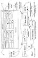
- Figure 3 illustrates a specific example where an error has occurred, is detected and subsequently corrected.
- the first value (value data 0) of a PDI is stored at a PDI node 30 whose last word or pointer field is at address 0014.
- a pointer to the last word of the node 30 is stored in the PDI table 9.
- the computer 2 finds the pointer for the PDI in the table 9 and checks the pointer field 31 to discover that the node 30 contains the immediately preceding value of the PDI.
- the next value is written into the value field of the node 32 and the address 1234 is entered in the pointer field 31 at the node 30 (all pointers are expressed in hexadecimal).
- the counter 10 is updated as described hereinbefore.
- the computer 2 When the next value (value data 2) of the same PDI is to be stored, the computer 2 follows the trail of pointers and determines that the node 32 contains the immediately preceding value. The next available space for a node in the memory segment is located and a node is allocated with its pointer field at address 2200. Allocation of the node is performed by changing the lowest bit of the address 2200 to 0, thus leaving FFFE in the pointer field. The value data 2 are stored in the value field of the node 33 and the next non-zero bit of the counter 10 is set to zero.
- a pointer to the node 33 begins to be written into the pointer field of the node 32 but power is removed, for example by withdrawing the card 1 from the card reader, before this is completed so that an incompletely written pointer 2274 is present in the pointer field of the word 32.
- the binary value 0010001000000000 should have been written into the pointer field of the node 32 but, instead, the binary value 0010001001110100 was written because switching of the third, fifth, sixth and seventh bits from 1 to 0 was not performed before power was removed.
- a memory segment contains a critical write counter in which a flag is set at the end of each value storing operation and a further flag is set at the end of each pointer adding operation. This ensures that, during a critical write to update the pointer address, the critical write counter is indicating an odd value.
- a flag may be set in the critical write counter before the first pointer adding operation in the set of updates and a further flag set only after the final pointer adding operation in the set of updates. If power fails between the setting of the flag and the setting of the further flag, a search will occur at the next power up.
- the advantage with this approach is that the critical write counter is written only twice during the set, thus making the system faster at least in the case where the power does not fail.
- the critical writes counter 10 can be omitted.
- the computer 2 cannot tell, when power is reapplied, whether any pointer errors may have occurred and must therefore compare all of the stored pointer values with the address of the LUM. If a pointer value is higher than the address of the LUM, the error is detected and can be corrected as described hereinbefore.
- this modified technique there is no penalty in terms of reduced memory capacity but more time is required by the computer 2 to search for any errors.
- each segment has its own LUM and is used to store a subset of the PDIs.
- each counter may be provided for each active page.
- each page may be partitioned with a separate critical writes counter for each partition. Searching and correcting an error in each partition is quicker but more memory space is required by several critical writes counters and each counter must be checked when power is applied to determine whether an error is present in the respective partition.
- the critical writes counter may also be treated as a PDI by allocating it in segments.
- the last item in the update chain is then the active block of the counter. This allows a smaller amount of memory to be initially allocated to the counter and, if the segment subsequently fills with a small number of large PDIs, then little space is wasted.
- the critical writes counter may be stored in the segment to which it relates or may be stored in a different segment. In the former case, it is important to ensure that new critical write counter segments are not allocated in the middle of another critical update. Otherwise, the LUM which the other update is using will have changed. To avoid this, the new critical write counter segment may be allocated a few updates earlier than required and not when a critical update is being performed.
- This technique may also be applied to flash memories of the type which are reset such that all of their bits are at 0 and writing to the memory involves changing the value of a bit from 0 to 1.
- all pointers may be stored in inverse or complementary form and may be reinverted when being read.
- the first value to be stored may be allocated to the node of highest address with subsequent values being allocated to and stored at the next lower address. The word of lowest address at each node is used as the pointer field. In this case, if a pointer value is incorrectly written, it will point to an address which is lower than that of the LUM. Thus, an erroneous pointer can be detected and its value corrected.
- the present invention relates to a method of and an apparatus for detecting an error in writing to persistent memory.
- the invention also relates to a method of and an apparatus for correcting the result of such an error.
- Such techniques may be used in embedded systems and examples of suitable applications include: smart cards such as Java Cards; digital active storage or security devices such as smart keys and smart disks; SIMs and USIMs for mobile telephones; data logging devices; small devices which record user preferences, store settings or log usage; computer systems in vehicles; set-top boxes; and internet routers.
- Such techniques are useful for persistent or "non-volatile" memories of the "write-once-erase-in-bulk” type, such as flash memory, and of the "write-only” type.
Landscapes
- Engineering & Computer Science (AREA)
- Theoretical Computer Science (AREA)
- Physics & Mathematics (AREA)
- General Engineering & Computer Science (AREA)
- General Physics & Mathematics (AREA)
- Human Computer Interaction (AREA)
- Quality & Reliability (AREA)
- Computer Security & Cryptography (AREA)
- Techniques For Improving Reliability Of Storages (AREA)
- Debugging And Monitoring (AREA)
- Read Only Memory (AREA)
Claims (30)
- Verfahren zur Erkennung von Fehlern in einem nichtflüchtigen Speichersegment, in dem Werte von wenigstens einem Datenelement in zeitweise aufeinanderfolgend angeordneten Speicherorten (15, 17, 18, 19; 30, 32, 33) gespeichert sind, wobei jeder neue Speicherort an ein erstes Ende eines Speicherblocks des Speichersegmentes, das erste und zweite Enden aufweist, hinzugefügt wird, und ein Pointer (31) zu jedem neuen Speicherort an einen alten Speicherort in dem Speicherblock, der einen vorhergehenden Wert von wenigstens einem Datenelement beinhaltet, hinzugefügt wird, wobei das Verfahren dadurch gekennzeichnet ist, dass es umfasst:(a) Bestimmen (24) der Adresse (2274), auf die der zuletzt hinzugefügte Pointer zeigt;(b) Vergleichen (25) der bestimmten Adresse (2274) mit einem Adressbereich (2200) des Speicherblocks, der den letzten neuen Speicherort (LUM) beinhaltet; und(c) Durchführen einer Aktion (27), wenn sich die bestimmte Adresse (2274) außerhalb des Adressbereiches (2200) befindet.
- Verfahren nach Anspruch 1, dadurch gekennzeichnet, dass die Schritte (a) bis (c) jedesmal ausgeführt werden, wenn Strom an das Speichersegment angelegt ist.
- Verfahren nach Anspruch 1 oder 2, dadurch gekennzeichnet, dass der Schritt (a) das Bestimmen der Adressen, auf die alle Pointer zeigen, und das Auswählen der höchsten oder niedrigsten Adresse umfasst.
- Verfahren nach Anspruch 1, 2 oder 3, dadurch gekennzeichnet, dass der Schritt (c) das Verändern der Adresse des zuletzt hinzugefügten Pointers in die Adresse des letzten neuen Speicherortes umfasst.
- Verfahren nach einem der vorhergehenden Ansprüche, dadurch gekennzeichnet, dass jeder neue Speicherort angrenzend an das erste Ende des Speicherblockes hinzugefügt wird.
- Verfahren nach einem- der vorhergehenden Ansprüche, dadurch gekennzeichnet, dass jeder Pointer auf eine höchste oder niedrigste Adresse des Speicherortes zeigt, auf den er zeigt.
- Verfahren nach einem der vorhergehenden Ansprüche, dadurch gekennzeichnet, dass das Speichersegment wenigstens einen Teil eines Flash-Speichers umfasst.
- Verfahren nach einem der vorhergehenden Ansprüche, dadurch gekennzeichnet, dass jeder Speicherort Raum für einen einzelnen Wert des wenigstens einen Datenelements aufweist.
- Verfahren nach einem der vorhergehenden Ansprüche, dadurch gekennzeichnet, dass jedes Bit des Speichersegmentes individuell nur von 1 auf 0 schaltbar ist, und dass die Aktion durchgeführt wird, wenn die erkannte Adresse größer ist als die höchste Adresse des Adressbereiches.
- Verfahren nach einem der Ansprüche 1 bis 8, dadurch gekennzeichnet, dass jedes Bit des Speichersegmentes individuell nur von 0 auf 1 schaltbar ist, und dass die Aktion durchgeführt wird, wenn die erkannte Adresse niedriger ist als die niedrigste Adresse des Adressbereiches.
- Verfahren nach einem der vorhergehenden Ansprüche, dadurch gekennzeichnet, dass das Speichersegment wenigstens einen Schreibzähler beinhaltet, in dem ein entsprechendes Flag an dem Ende jedes WertSpeichervorganges gesetzt wird, und ein entsprechendes weiteres Flag an dem Ende jeder Pointer-Hinzufügung gesetzt wird, und auch dadurch gekennzeichnet, dass die Schritte (a) bis (c) nur durchgeführt werden, wenn eine ungerade Anzahl von Flags und weiteren Flags gesetzt ist.
- Verfahren nach Anspruch 11, dadurch gekennzeichnet, dass wenigstens ein Schreibzähler ein Datenelement umfasst.
- Verfahren nach einem der vorhergehenden Ansprüche, dadurch gekennzeichnet, dass das Speichersegment wenigstens einen Schreibzähler beinhaltet, in dem, wenn er eine Reihe von einem oder mehreren Datenelement-Werte speichert, ein entsprechendes Flag vor der ersten Pointer-Hinzufügung in der Reihe gesetzt wird und ein entsprechendes weiteres Flag nach der letzten Pointer-Hinzufügung in der Reihe gesetzt wird, und auch dadurch gekennzeichnet, dass die Schritte (a) bis (c) nur durchgeführt werden, wenn eine ungerade Anzahl von Flags oder weiteren Flags gesetzt ist.
- Programm zum Steuern eines Computers, um ein Verfahren durchzuführen, wie es in einem der vorhergehenden Ansprüche beansprucht ist.
- Computer, der durch ein Programm nach Anspruch 14 programmiert ist.
- Speichermedium, das ein Programm nach Anspruch 14 beinhaltet.
- Eine Vorrichtung, die ein nichtflüchtiges Speichersegment, Mittel, um Werte von wenigstens einem Datenelement in zeitweise aufeinanderfolgend angeordneten Speicherorten (15, 17, 18, 19; 30, 32, 33) zu speichern, wobei jeder neuen Speicherort an einem ersten Ende eines Speicherblockes des Speichersegmentes hinzugefügt wird, das erste und zweite Enden aufweist, Mittel, um einen Pointer (31) hinzuzufügen, der auf jeden neuen Speicherort auf einen alten Speicherort in dem Speicherblock zeigt, der einen vorgegebenen Wert von wenigstens einem Datenelement beinhaltet, aufweist, und durch Mittel gekennzeichnet ist, zum Bestimmen (24) der Adresse (2274), auf die der zuletzt hinzugefügte Pointer zeigt, Mittel zum Vergleichen (25) der bestimmten Adresse (2274) mit einem Adressbereich (2200) des Speicherblocks, der den letzten neuen Speicherort (LUM) enthält, und Mittel zum Durchführen einer Aktion (27), wenn sich die bestimmte Adresse (2274) außerhalb des Adressbereiches (2200) befindet.
- Vorrichtung nach Anspruch 17, dadurch gekennzeichnet, dass die Bestimmungsmittel, die Vergleichsmittel und die Ausführungsmittel angeordnet sind, um jedesmal betätigt zu werden, wenn Strom an der Vorrichtung angelegt ist.
- Vorrichtung nach Anspruch 17 oder 18, dadurch gekennzeichnet, dass die Bestimmungsmittel angeordnet sind, um die Adressen zu bestimmen, auf die alle Pointer zeigen, und um die höchste oder niedrigste Adresse auszuwählen.
- Vorrichtung nach Anspruch 17, 18 oder 19, dadurch gekennzeichnet, dass die Ausführungsmittel angeordnet sind, um die Adresse des zuletzt hinzugefügten Pointers in die Adresse des letzten neuen Speicherortes zu ändern.
- Vorrichtung nach einem der Ansprüche 17 bis 20, dadurch gekennzeichnet, dass jeder neue Speicherort angrenzend an das erste Ende des Speicherblocks hinzugefügt wird.
- Vorrichtung nach einem der Ansprüche 17 bis 21, dadurch gekennzeichnet, dass jeder Pointer auf eine höchste oder niedrigste Adresse des Speicherortes zeigt, auf die er zeigt.
- Vorrichtung nach einem der Ansprüche 17 bis 22, dadurch gekennzeichnet, dass das Speichersegment wenigstens einen Teil des Flash-Speichers umfasst.
- Vorrichtung nach einem der Ansprüche 17 bis 23, dadurch gekennzeichnet, dass jeder Speicherort Raum für einen einzelnen Wert von wenigstens einem Datenelement aufweist.
- Vorrichtung nach einem der Ansprüche 17 bis 24, dadurch gekennzeichnet, dass jedes Bit des Speichersegmentes individuell nur von 1 oder 0 schaltbar ist und die Ausführungsmittel angeordnet sind, um die Aktion durchzuführen, wenn die erkannte Adresse größer ist als die höchste Adresse des Adressbereiches.
- Vorrichtung nach einem der Ansprüche 17 bis 24, dadurch gekennzeichnet, dass jedes Bit des Speichersegmentes individuell nur von 0 auf 1 schaltbar ist, und dass die Ausführungsmittel angeordnet sind, um die Aktion auszuführen, wenn die erkannte Adresse niedriger ist als die niedrigste Adresse des Adressbereiches.
- Vorrichtung nach einem der Ansprüche 17 bis 26, dadurch gekennzeichnet, dass sie umfasst: Mittel, um in wenigstens einem Schreibzähler in dem Speichersegment ein entsprechendes Flag an dem Anfang jedes Wertspeichervorganges und ein entsprechendes weiteres Flag an dem Ende jeder Pointer-Hinzufügung zu setzen; und Mittel, um zu beurteilen, ob die Anzahl der gesetzten Flags und der weiteren Flags ungerade ist, wobei die Bestimmungsmittel, die Vergleichsmittel und die Ausführungsmittel angeordnet sind, um als Antwort auf die Beurteilungsmittel betrieben zu werden.
- Vorrichtung nach Anspruch 27, dadurch gekennzeichnet, dass wenigstens ein Schreibzähler ein Datenelement umfasst.
- Vorrichtung nach einem der Ansprüche 17 bis 28, dadurch gekennzeichnet, dass sie umfasst: Mittel, um in wenigstens einem Schreibzähler in dem Speichersegment und, wenn eine Reihe von einem oder mehreren Datenelementwerten gespeichert werden, ein entsprechendes Flag vor der ersten Pointer-Hinzufügung in der Reihe und ein entsprechendes weiteres Flag nach der letzten Pointer-Hinzufügung in der Reihe zu setzen; und Mittel, um zu beurteilen, ob die Anzahl der gesetzten Flags oder der weiteren Flags ungerade ist, wobei die Bestimmungsmittel, die Vergleichsmittel und die Ausführungsmittel angeordnet sind, um als Antwort auf die Beurteilungsmittel betrieben zu werden.
- Vorrichtung nach einem der Ansprüche 17 bis 29, dadurch gekennzeichnet, dass sie eine Chipkarte umfasst.
Applications Claiming Priority (3)
| Application Number | Priority Date | Filing Date | Title |
|---|---|---|---|
| GB0221868 | 2002-09-20 | ||
| GB0221868A GB2393273A (en) | 2002-09-20 | 2002-09-20 | Method and apparatus for detecting an error in writing to persistent memory |
| PCT/JP2003/011789 WO2004027615A2 (en) | 2002-09-20 | 2003-09-16 | Method of and apparatus for detecting an error in writing to persistent memory |
Publications (2)
| Publication Number | Publication Date |
|---|---|
| EP1540660A2 EP1540660A2 (de) | 2005-06-15 |
| EP1540660B1 true EP1540660B1 (de) | 2007-11-28 |
Family
ID=9944459
Family Applications (1)
| Application Number | Title | Priority Date | Filing Date |
|---|---|---|---|
| EP03797616A Expired - Lifetime EP1540660B1 (de) | 2002-09-20 | 2003-09-16 | Verfahren und vorrichtung zur erkennung von fehlern während des schreibens in einen nichtflüchtigen speicher |
Country Status (9)
| Country | Link |
|---|---|
| US (1) | US7539905B2 (de) |
| EP (1) | EP1540660B1 (de) |
| JP (1) | JP4329937B2 (de) |
| CN (1) | CN1695206A (de) |
| AT (1) | ATE379837T1 (de) |
| AU (1) | AU2003263600A1 (de) |
| DE (1) | DE60317801T2 (de) |
| GB (1) | GB2393273A (de) |
| WO (1) | WO2004027615A2 (de) |
Families Citing this family (12)
| Publication number | Priority date | Publication date | Assignee | Title |
|---|---|---|---|---|
| WO2004066571A1 (ja) * | 2003-01-20 | 2004-08-05 | Fujitsu Limited | ネットワークスイッチ装置およびネットワークスイッチ方法 |
| US7475209B2 (en) * | 2004-05-13 | 2009-01-06 | International Business Machines Corporation | Moving hardware context structures in memory while maintaining system operation |
| US7743277B2 (en) * | 2005-02-14 | 2010-06-22 | Stec, Inc. | System and method for detecting and reducing data corruption in a storage device |
| US8533562B2 (en) * | 2007-09-12 | 2013-09-10 | Sandisk Technologies Inc. | Data protection after possible write abort or erase abort |
| EP2270758B1 (de) * | 2009-06-30 | 2013-11-27 | Kabushiki Kaisha Toshiba | Tragbare elektronische Vorrichtung, Verarbeitungsvorrichtung für die tragbare elektronische Vorrichtung und Datenverarbeitungsverfahren in einer tragbare elektronischen Vorrichtung |
| US8321481B2 (en) * | 2010-05-13 | 2012-11-27 | Assa Abloy Ab | Method for incremental anti-tear garbage collection |
| US9116634B2 (en) * | 2011-06-10 | 2015-08-25 | International Business Machines Corporation | Configure storage class memory command |
| CN103310848A (zh) * | 2012-03-08 | 2013-09-18 | 鼎桥通信技术有限公司 | 一种使用存储器的方法和装置 |
| US9208040B2 (en) * | 2014-04-30 | 2015-12-08 | Stmicroelectronics International N.V. | Repair control logic for safe memories having redundant elements |
| WO2017048261A1 (en) | 2015-09-17 | 2017-03-23 | Hewlett Packard Enterprise Development Lp | Memory store error check |
| CN108108413B (zh) * | 2017-12-12 | 2022-04-26 | 宁波三星医疗电气股份有限公司 | 一种基于存储数据自动生成数据指针的方法及系统 |
| CN114879913A (zh) * | 2022-05-30 | 2022-08-09 | 重庆大学 | 一种eeprom数据可靠存储的方法 |
Family Cites Families (19)
| Publication number | Priority date | Publication date | Assignee | Title |
|---|---|---|---|---|
| EP0398545A1 (de) | 1989-05-19 | 1990-11-22 | Delco Electronics Corporation | Verfahren und Vorrichtung zur Datenspeicherung in einem nichtflüchtigen Speicher |
| US5369757A (en) * | 1991-06-18 | 1994-11-29 | Digital Equipment Corporation | Recovery logging in the presence of snapshot files by ordering of buffer pool flushing |
| US5469562A (en) * | 1992-06-26 | 1995-11-21 | Digital Equipment Corporation | Durable atomic storage update manager |
| US5873097A (en) * | 1993-05-12 | 1999-02-16 | Apple Computer, Inc. | Update mechanism for computer storage container manager |
| US5644709A (en) * | 1994-04-21 | 1997-07-01 | Wisconsin Alumni Research Foundation | Method for detecting computer memory access errors |
| US5530806A (en) * | 1994-12-15 | 1996-06-25 | At&T Corp. | Method and apparatus for storing and retrieving routing information in a network node |
| GB2317722B (en) * | 1996-09-30 | 2001-07-18 | Nokia Mobile Phones Ltd | Memory device |
| GB9801373D0 (en) * | 1998-01-22 | 1998-03-18 | Memory Corp Plc | Memory system |
| US6247108B1 (en) * | 1998-06-03 | 2001-06-12 | Lucent Technologies Inc. | Memory management during processing of binary decision diagrams in a computer system |
| US6412080B1 (en) * | 1999-02-23 | 2002-06-25 | Microsoft Corporation | Lightweight persistent storage system for flash memory devices |
| DE19921232B4 (de) * | 1999-05-07 | 2007-06-21 | Giesecke & Devrient Gmbh | Verfahren zum gesicherten Schreiben eines Zeigers für einen Ringspeicher, zugehöriger Ringspeicher, Verwendung des Ringspeichers und Chipkarte mit Ringspeicher |
| DE10059006B4 (de) * | 1999-12-30 | 2004-04-15 | International Business Machines Corp. | Verfahren und System zur sicheren Verwaltung von Dateien in nichtflüchtigen Speichern |
| JP2002062956A (ja) * | 2000-08-21 | 2002-02-28 | Sankyo Seiki Mfg Co Ltd | 停電処理方法及び停電処理装置 |
| US6977941B2 (en) * | 2000-11-08 | 2005-12-20 | Hitachi, Ltd. | Shared buffer type variable length packet switch |
| US6928456B2 (en) * | 2001-03-06 | 2005-08-09 | Intel Corporation | Method of tracking objects for application modifications |
| JP2002278850A (ja) | 2001-03-14 | 2002-09-27 | Nec Corp | 半導体装置 |
| US6779084B2 (en) * | 2002-01-23 | 2004-08-17 | Intel Corporation | Enqueue operations for multi-buffer packets |
| US7131115B2 (en) * | 2002-03-25 | 2006-10-31 | Hewlett-Packard Development Company, L.P. | Unwinding instrumented program code |
| US7337275B2 (en) * | 2002-08-13 | 2008-02-26 | Intel Corporation | Free list and ring data structure management |
-
2002
- 2002-09-20 GB GB0221868A patent/GB2393273A/en not_active Withdrawn
-
2003
- 2003-09-16 JP JP2004537573A patent/JP4329937B2/ja not_active Expired - Fee Related
- 2003-09-16 AU AU2003263600A patent/AU2003263600A1/en not_active Abandoned
- 2003-09-16 DE DE60317801T patent/DE60317801T2/de not_active Expired - Lifetime
- 2003-09-16 CN CN03825131.0A patent/CN1695206A/zh active Pending
- 2003-09-16 US US10/528,328 patent/US7539905B2/en not_active Expired - Fee Related
- 2003-09-16 EP EP03797616A patent/EP1540660B1/de not_active Expired - Lifetime
- 2003-09-16 AT AT03797616T patent/ATE379837T1/de not_active IP Right Cessation
- 2003-09-16 WO PCT/JP2003/011789 patent/WO2004027615A2/en not_active Ceased
Also Published As
| Publication number | Publication date |
|---|---|
| US20060143541A1 (en) | 2006-06-29 |
| AU2003263600A1 (en) | 2004-04-08 |
| DE60317801D1 (de) | 2008-01-10 |
| WO2004027615A2 (en) | 2004-04-01 |
| EP1540660A2 (de) | 2005-06-15 |
| JP2006500653A (ja) | 2006-01-05 |
| GB2393273A (en) | 2004-03-24 |
| AU2003263600A8 (en) | 2004-04-08 |
| WO2004027615A3 (en) | 2004-07-01 |
| JP4329937B2 (ja) | 2009-09-09 |
| GB0221868D0 (en) | 2002-10-30 |
| ATE379837T1 (de) | 2007-12-15 |
| US7539905B2 (en) | 2009-05-26 |
| DE60317801T2 (de) | 2008-10-30 |
| CN1695206A (zh) | 2005-11-09 |
Similar Documents
| Publication | Publication Date | Title |
|---|---|---|
| CN105975399B (zh) | 用来管理一记忆装置的方法以及其相关的记忆装置 | |
| US6449625B1 (en) | Use of a two-way stack approach to optimize flash memory management for embedded database systems | |
| US6839823B1 (en) | Increased reliability of data stored on flash memory in applications sensitive to power-loss | |
| US5987478A (en) | Virtual small block file manager for flash memory array | |
| KR100493732B1 (ko) | 비휘발성 메모리내의 코드/데이터 경계를 조정가능하게하는 장치 및 방법 | |
| JP3242890B2 (ja) | 記憶装置 | |
| US6104638A (en) | Use of erasable non-volatile memory for storage of changing information | |
| EP1540660B1 (de) | Verfahren und vorrichtung zur erkennung von fehlern während des schreibens in einen nichtflüchtigen speicher | |
| US20020041517A1 (en) | Method of driving remapping in flash memory and flash memory architecture suitable therefor | |
| EP2003569A2 (de) | Flashspeichersteuerung | |
| US20050036390A1 (en) | Non-volatile memory and non-volatile memory data rewriting method | |
| KR19990087236A (ko) | 부분불량메모리를 탑재한 반도체기억장치 | |
| WO1997012324A1 (en) | Memory management | |
| US20010054129A1 (en) | Method, system and computer program | |
| KR19990029196A (ko) | 반도체 기억 장치 및 그 데이터 관리 방법 | |
| KR20040076589A (ko) | 메모리 카드 | |
| CN112612418A (zh) | 一种用于大容量NandFlash坏块管理的方法及系统 | |
| CN109240622A (zh) | 一种eeprom数据写入的方法及系统 | |
| CN111324549B (zh) | 一种存储器及其控制方法和装置 | |
| KR101826778B1 (ko) | 플래쉬 라이프 사이클 및 성능 개선을 고려한 eeprom 에뮬레이션 구현 방법 | |
| CN113253934A (zh) | Flash坏块处理方法、装置、计算机设备和可读存储介质 | |
| US20040186962A1 (en) | Method, system, and computer-readable medium for updating memory devices in a computer system | |
| EP4379723A1 (de) | Nichtflüchtiger speicher | |
| JP2003036209A (ja) | 不揮発性メモリ並びに不揮発性メモリのデータ書き換え方法 | |
| JPH04123243A (ja) | データ書込装置 |
Legal Events
| Date | Code | Title | Description |
|---|---|---|---|
| PUAI | Public reference made under article 153(3) epc to a published international application that has entered the european phase |
Free format text: ORIGINAL CODE: 0009012 |
|
| 17P | Request for examination filed |
Effective date: 20050323 |
|
| AK | Designated contracting states |
Kind code of ref document: A2 Designated state(s): AT BE BG CH CY CZ DE DK EE ES FI FR GB GR HU IE IT LI LU MC NL PT RO SE SI SK TR |
|
| AX | Request for extension of the european patent |
Extension state: AL LT LV MK |
|
| DAX | Request for extension of the european patent (deleted) | ||
| GRAP | Despatch of communication of intention to grant a patent |
Free format text: ORIGINAL CODE: EPIDOSNIGR1 |
|
| GRAC | Information related to communication of intention to grant a patent modified |
Free format text: ORIGINAL CODE: EPIDOSCIGR1 |
|
| GRAS | Grant fee paid |
Free format text: ORIGINAL CODE: EPIDOSNIGR3 |
|
| GRAA | (expected) grant |
Free format text: ORIGINAL CODE: 0009210 |
|
| AK | Designated contracting states |
Kind code of ref document: B1 Designated state(s): AT BE BG CH CY CZ DE DK EE ES FI FR GB GR HU IE IT LI LU MC NL PT RO SE SI SK TR |
|
| REG | Reference to a national code |
Ref country code: GB Ref legal event code: FG4D |
|
| REG | Reference to a national code |
Ref country code: IE Ref legal event code: FG4D |
|
| REG | Reference to a national code |
Ref country code: CH Ref legal event code: EP |
|
| REF | Corresponds to: |
Ref document number: 60317801 Country of ref document: DE Date of ref document: 20080110 Kind code of ref document: P |
|
| PG25 | Lapsed in a contracting state [announced via postgrant information from national office to epo] |
Ref country code: LI Free format text: LAPSE BECAUSE OF FAILURE TO SUBMIT A TRANSLATION OF THE DESCRIPTION OR TO PAY THE FEE WITHIN THE PRESCRIBED TIME-LIMIT Effective date: 20071128 Ref country code: CH Free format text: LAPSE BECAUSE OF FAILURE TO SUBMIT A TRANSLATION OF THE DESCRIPTION OR TO PAY THE FEE WITHIN THE PRESCRIBED TIME-LIMIT Effective date: 20071128 Ref country code: ES Free format text: LAPSE BECAUSE OF FAILURE TO SUBMIT A TRANSLATION OF THE DESCRIPTION OR TO PAY THE FEE WITHIN THE PRESCRIBED TIME-LIMIT Effective date: 20080311 Ref country code: SE Free format text: LAPSE BECAUSE OF FAILURE TO SUBMIT A TRANSLATION OF THE DESCRIPTION OR TO PAY THE FEE WITHIN THE PRESCRIBED TIME-LIMIT Effective date: 20080228 Ref country code: NL Free format text: LAPSE BECAUSE OF FAILURE TO SUBMIT A TRANSLATION OF THE DESCRIPTION OR TO PAY THE FEE WITHIN THE PRESCRIBED TIME-LIMIT Effective date: 20071128 |
|
| NLV1 | Nl: lapsed or annulled due to failure to fulfill the requirements of art. 29p and 29m of the patents act | ||
| PG25 | Lapsed in a contracting state [announced via postgrant information from national office to epo] |
Ref country code: BG Free format text: LAPSE BECAUSE OF FAILURE TO SUBMIT A TRANSLATION OF THE DESCRIPTION OR TO PAY THE FEE WITHIN THE PRESCRIBED TIME-LIMIT Effective date: 20080228 Ref country code: SI Free format text: LAPSE BECAUSE OF FAILURE TO SUBMIT A TRANSLATION OF THE DESCRIPTION OR TO PAY THE FEE WITHIN THE PRESCRIBED TIME-LIMIT Effective date: 20071128 Ref country code: FI Free format text: LAPSE BECAUSE OF FAILURE TO SUBMIT A TRANSLATION OF THE DESCRIPTION OR TO PAY THE FEE WITHIN THE PRESCRIBED TIME-LIMIT Effective date: 20071128 |
|
| REG | Reference to a national code |
Ref country code: CH Ref legal event code: PL |
|
| PG25 | Lapsed in a contracting state [announced via postgrant information from national office to epo] |
Ref country code: AT Free format text: LAPSE BECAUSE OF FAILURE TO SUBMIT A TRANSLATION OF THE DESCRIPTION OR TO PAY THE FEE WITHIN THE PRESCRIBED TIME-LIMIT Effective date: 20071128 |
|
| PG25 | Lapsed in a contracting state [announced via postgrant information from national office to epo] |
Ref country code: CZ Free format text: LAPSE BECAUSE OF FAILURE TO SUBMIT A TRANSLATION OF THE DESCRIPTION OR TO PAY THE FEE WITHIN THE PRESCRIBED TIME-LIMIT Effective date: 20071128 Ref country code: DK Free format text: LAPSE BECAUSE OF FAILURE TO SUBMIT A TRANSLATION OF THE DESCRIPTION OR TO PAY THE FEE WITHIN THE PRESCRIBED TIME-LIMIT Effective date: 20071128 |
|
| ET | Fr: translation filed | ||
| PG25 | Lapsed in a contracting state [announced via postgrant information from national office to epo] |
Ref country code: RO Free format text: LAPSE BECAUSE OF FAILURE TO SUBMIT A TRANSLATION OF THE DESCRIPTION OR TO PAY THE FEE WITHIN THE PRESCRIBED TIME-LIMIT Effective date: 20071128 Ref country code: SK Free format text: LAPSE BECAUSE OF FAILURE TO SUBMIT A TRANSLATION OF THE DESCRIPTION OR TO PAY THE FEE WITHIN THE PRESCRIBED TIME-LIMIT Effective date: 20071128 Ref country code: BE Free format text: LAPSE BECAUSE OF FAILURE TO SUBMIT A TRANSLATION OF THE DESCRIPTION OR TO PAY THE FEE WITHIN THE PRESCRIBED TIME-LIMIT Effective date: 20071128 |
|
| PG25 | Lapsed in a contracting state [announced via postgrant information from national office to epo] |
Ref country code: PT Free format text: LAPSE BECAUSE OF FAILURE TO SUBMIT A TRANSLATION OF THE DESCRIPTION OR TO PAY THE FEE WITHIN THE PRESCRIBED TIME-LIMIT Effective date: 20080428 |
|
| PLBE | No opposition filed within time limit |
Free format text: ORIGINAL CODE: 0009261 |
|
| STAA | Information on the status of an ep patent application or granted ep patent |
Free format text: STATUS: NO OPPOSITION FILED WITHIN TIME LIMIT |
|
| 26N | No opposition filed |
Effective date: 20080829 |
|
| PG25 | Lapsed in a contracting state [announced via postgrant information from national office to epo] |
Ref country code: GR Free format text: LAPSE BECAUSE OF FAILURE TO SUBMIT A TRANSLATION OF THE DESCRIPTION OR TO PAY THE FEE WITHIN THE PRESCRIBED TIME-LIMIT Effective date: 20080229 |
|
| PG25 | Lapsed in a contracting state [announced via postgrant information from national office to epo] |
Ref country code: EE Free format text: LAPSE BECAUSE OF FAILURE TO SUBMIT A TRANSLATION OF THE DESCRIPTION OR TO PAY THE FEE WITHIN THE PRESCRIBED TIME-LIMIT Effective date: 20071128 Ref country code: MC Free format text: LAPSE BECAUSE OF NON-PAYMENT OF DUE FEES Effective date: 20080930 |
|
| PG25 | Lapsed in a contracting state [announced via postgrant information from national office to epo] |
Ref country code: IE Free format text: LAPSE BECAUSE OF NON-PAYMENT OF DUE FEES Effective date: 20080916 Ref country code: CY Free format text: LAPSE BECAUSE OF FAILURE TO SUBMIT A TRANSLATION OF THE DESCRIPTION OR TO PAY THE FEE WITHIN THE PRESCRIBED TIME-LIMIT Effective date: 20071128 |
|
| PG25 | Lapsed in a contracting state [announced via postgrant information from national office to epo] |
Ref country code: HU Free format text: LAPSE BECAUSE OF FAILURE TO SUBMIT A TRANSLATION OF THE DESCRIPTION OR TO PAY THE FEE WITHIN THE PRESCRIBED TIME-LIMIT Effective date: 20080529 Ref country code: LU Free format text: LAPSE BECAUSE OF NON-PAYMENT OF DUE FEES Effective date: 20080916 |
|
| PG25 | Lapsed in a contracting state [announced via postgrant information from national office to epo] |
Ref country code: TR Free format text: LAPSE BECAUSE OF FAILURE TO SUBMIT A TRANSLATION OF THE DESCRIPTION OR TO PAY THE FEE WITHIN THE PRESCRIBED TIME-LIMIT Effective date: 20071128 |
|
| PG25 | Lapsed in a contracting state [announced via postgrant information from national office to epo] |
Ref country code: IT Free format text: LAPSE BECAUSE OF NON-PAYMENT OF DUE FEES Effective date: 20080930 |
|
| REG | Reference to a national code |
Ref country code: FR Ref legal event code: PLFP Year of fee payment: 13 |
|
| PGFP | Annual fee paid to national office [announced via postgrant information from national office to epo] |
Ref country code: GB Payment date: 20150917 Year of fee payment: 13 Ref country code: DE Payment date: 20150922 Year of fee payment: 13 |
|
| PGFP | Annual fee paid to national office [announced via postgrant information from national office to epo] |
Ref country code: FR Payment date: 20150922 Year of fee payment: 13 |
|
| REG | Reference to a national code |
Ref country code: DE Ref legal event code: R119 Ref document number: 60317801 Country of ref document: DE |
|
| GBPC | Gb: european patent ceased through non-payment of renewal fee |
Effective date: 20160916 |
|
| REG | Reference to a national code |
Ref country code: FR Ref legal event code: ST Effective date: 20170531 |
|
| PG25 | Lapsed in a contracting state [announced via postgrant information from national office to epo] |
Ref country code: FR Free format text: LAPSE BECAUSE OF NON-PAYMENT OF DUE FEES Effective date: 20160930 Ref country code: DE Free format text: LAPSE BECAUSE OF NON-PAYMENT OF DUE FEES Effective date: 20170401 Ref country code: GB Free format text: LAPSE BECAUSE OF NON-PAYMENT OF DUE FEES Effective date: 20160916 |