EP1540649B1 - Tete de balayage optique et son procede de production - Google Patents
Tete de balayage optique et son procede de production Download PDFInfo
- Publication number
- EP1540649B1 EP1540649B1 EP03798045A EP03798045A EP1540649B1 EP 1540649 B1 EP1540649 B1 EP 1540649B1 EP 03798045 A EP03798045 A EP 03798045A EP 03798045 A EP03798045 A EP 03798045A EP 1540649 B1 EP1540649 B1 EP 1540649B1
- Authority
- EP
- European Patent Office
- Prior art keywords
- substrate
- sensing head
- optical
- signal detector
- head according
- Prior art date
- Legal status (The legal status is an assumption and is not a legal conclusion. Google has not performed a legal analysis and makes no representation as to the accuracy of the status listed.)
- Expired - Lifetime
Links
Images


Classifications
-
- G—PHYSICS
- G11—INFORMATION STORAGE
- G11B—INFORMATION STORAGE BASED ON RELATIVE MOVEMENT BETWEEN RECORD CARRIER AND TRANSDUCER
- G11B7/00—Recording or reproducing by optical means, e.g. recording using a thermal beam of optical radiation by modifying optical properties or the physical structure, reproducing using an optical beam at lower power by sensing optical properties; Record carriers therefor
- G11B7/12—Heads, e.g. forming of the optical beam spot or modulation of the optical beam
- G11B7/125—Optical beam sources therefor, e.g. laser control circuitry specially adapted for optical storage devices; Modulators, e.g. means for controlling the size or intensity of optical spots or optical traces
- G11B7/126—Circuits, methods or arrangements for laser control or stabilisation
- G11B7/1263—Power control during transducing, e.g. by monitoring
-
- G—PHYSICS
- G11—INFORMATION STORAGE
- G11B—INFORMATION STORAGE BASED ON RELATIVE MOVEMENT BETWEEN RECORD CARRIER AND TRANSDUCER
- G11B7/00—Recording or reproducing by optical means, e.g. recording using a thermal beam of optical radiation by modifying optical properties or the physical structure, reproducing using an optical beam at lower power by sensing optical properties; Record carriers therefor
- G11B7/12—Heads, e.g. forming of the optical beam spot or modulation of the optical beam
- G11B7/123—Integrated head arrangements, e.g. with source and detectors mounted on the same substrate
-
- G—PHYSICS
- G11—INFORMATION STORAGE
- G11B—INFORMATION STORAGE BASED ON RELATIVE MOVEMENT BETWEEN RECORD CARRIER AND TRANSDUCER
- G11B7/00—Recording or reproducing by optical means, e.g. recording using a thermal beam of optical radiation by modifying optical properties or the physical structure, reproducing using an optical beam at lower power by sensing optical properties; Record carriers therefor
- G11B7/12—Heads, e.g. forming of the optical beam spot or modulation of the optical beam
- G11B7/22—Apparatus or processes for the manufacture of optical heads, e.g. assembly
-
- G—PHYSICS
- G02—OPTICS
- G02B—OPTICAL ELEMENTS, SYSTEMS OR APPARATUS
- G02B6/00—Light guides; Structural details of arrangements comprising light guides and other optical elements, e.g. couplings
- G02B6/24—Coupling light guides
- G02B6/42—Coupling light guides with opto-electronic elements
- G02B6/4201—Packages, e.g. shape, construction, internal or external details
- G02B6/4204—Packages, e.g. shape, construction, internal or external details the coupling comprising intermediate optical elements, e.g. lenses, holograms
- G02B6/4214—Packages, e.g. shape, construction, internal or external details the coupling comprising intermediate optical elements, e.g. lenses, holograms the intermediate optical element having redirecting reflective means, e.g. mirrors, prisms for deflecting the radiation from horizontal to down- or upward direction toward a device
Definitions
- the invention relates to an optical scanning head, in particular for reading an optical data memory and a method for producing such a scanning head.
- Optical devices for reading out data are known, for example, from the publications US 6,104,690 . US 6,385 . 157 B1 and EP 0 555 097 A1 known.
- a conventional optical pickup such as that used in a CD player or a DVD player, typically consists of discrete active and passive components that are manufactured individually and installed in a hybrid metal housing.
- a scanning head typically includes a laser source, optical components such as lenses and beamsplitters, a retarder plate and detectors for monitor and signal functions.
- the signal detector detects for measuring track, distance and signal level, the light emitted by the laser diode and the CD or DVD disc is reflected.
- the monitor detector is used to control the emitted laser power.
- the monitor detector is typically located near the laser source. For example, it can be provided that a part of the laser beam strikes a monitor photodiode directly behind a housed laser diode.
- the signal detector is typically mounted as a single component on the metal housing of the scanning head.
- Such a scanning head has a size of about 30 mm x 40 mm and is relatively large and heavy due to the discrete structure.
- the monitor detector and the signal detector are in separate housings and have to be individually adjusted.
- US-A-6 104690 shows an optical scanning head and a manufacturing method according to the preamble of claims 1 and 16.
- the object is to provide an optical pickup, which has a low weight and a small footprint and whose components can be easily matched. It is also a manufacturing method for such an optical pickup are given, which allows a cost-effective production and assembly.
- an optical pickup head of the type mentioned in the introduction has a substrate with a main surface, an edge emitting laser component arranged on the main surface of the substrate whose emission axis is directed essentially parallel to the first main plane, a deflection device arranged on the main surface of the substrate for redirecting the laser radiation in a direction substantially perpendicular to the main surface direction, at least one signal detector for detecting the laser radiation reflected from the optical data storage, and an optical element that guides the deflected laser radiation to the optical data storage and reflected laser radiation to the at least one signal detector, wherein the optical element is connected via at least one support member to the substrate, and wherein the optical element is characterized in that the at least one support element and / or the deflection device are made of glass, and the z around at least one support element and / or the deflection device are connected inextricably linked to the substrate by anodic bonding.
- a very small size and associated low weight of the scanhead can be achieved.
- This allows the use of the invention Scanning head especially for mobile applications, such as cameras, music players, game consoles, electronic books (eBooks), PDAs, laptops or computer peripherals.
- the integration allows the use of cost-effective manufacturing and assembly processes, so that the scanning head according to the invention can be made cheaper than conventional pickup systems. Due to the low weight of the scanning head faster access times can be achieved than with conventional pickup systems.
- the deflection device is at the same time designed as a support element, via which the optical element is connected to the substrate.
- a radiation direction signal detector is arranged on the main surface of the substrate on the emission axis of the laser component and in the emission direction behind the deflection device.
- the laser device, the deflection device and the emission direction signal detector are arranged in this order one behind the other on a straight line.
- an opposite direction signal detector is arranged on the main surface of the substrate on the emission axis of the laser component and opposite to the emission direction of the laser component.
- a support element is advantageously arranged, via which the optical element is connected to the substrate.
- the support element arranged between the laser component and the counter-directional signal detector is provided with a metallic or dielectric mirror layer on its surface facing the laser component.
- the support element arranged between the laser component and the opposite-direction signal detector may be provided with an absorption layer on its surface facing the laser component. Also, the scattered light coupling is effectively suppressed.
- the support element arranged between the laser component and the opposite-direction signal detector is designed as a deflection device which deflects the scattered light of the laser component away from the opposite-direction signal detector.
- the support element deflects the scattered light in a direction substantially perpendicular to the main surface.
- an optical scanning head according to the invention can be further increased by the fact that the at least one signal detector is formed in the substrate.
- the at least one signal detector comprises an array of PIN photodiodes formed in the substrate.
- a monitor detector for controlling the radiated power of the laser component is also integrated on the substrate.
- the support elements are arranged laterally of the deflection mirror and the detectors installed between the mirror and the support elements.
- the optical element is mounted on the support elements.
- the substrate is advantageously formed by a silicon substrate. Cost-effective processes of the semiconductor industry can then be used for the manufacturing and assembly processes.
- the major surface of the substrate preferably has an area of 10 mm 2 or less.
- trenches are preferably introduced into the rear side of the glass wafer by sandblasting prior to sawing the glass wafer.
- the support elements are produced at the same time as the deflection device from the glass wafer.
- an array of PIN photodiodes are formed in the substrate as the signal detector (s).
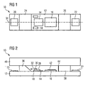
- FIG. 1 shows a plan view of a silicon submount designated generally by 10 before the assembly of the glass prisms
- FIG. 2 shows the submount 10 after assembly with laser and optics.
- the silicon submount 10 includes an about 1.3 mm x 4.8 mm silicon substrate 12 having chip bonding surfaces 14 and 16, two monitor photodiodes 18 and two signal diodes 20 and 22.
- chip bonding surface 14 On the chip bonding surface 14, a heat sink 28 and on the heat sink 28, an edge emitting laser diode 30 is mounted, which emits red laser radiation 32 along the emission axis 34 in operation.
- the chip bonding surface 16 carries an integrated circuit 42, such as an amplifier or laser driver circuit.
- two glass prisms 36 and 38 are inextricably connected to the substrate 12 by anodic bonding.
- the glass prisms serve as a support elements on which an optical component 40 is fixed, for example by soldering.
- the glass prism 36 further serves as a deflection prism, which deflects the laser radiation 32 emitted parallel to the surface of the substrate 12 along the emission axis 34 by 90 °.
- the optical component 40 leads the deflected laser radiation to an optical storage medium, not shown, and leads the laser radiation reflected there to the optical storage medium Signal diodes 20 and 22 back.
- the signals modulated according to a line or dot pattern on the storage medium are used after their detection by the signal diodes 20 and 22 in a conventional manner for data transmission, as well as for tracking and tracking.
- the glass prism 38 is mirrored on its surface facing the laser diode 30 with an aluminum layer 44 in order to prevent stray radiation from the laser diode 30 from reaching the signal diode 22.
- the glass prism may also be provided with another metallic layer, for example an AlSi layer, or with a dielectric mirror, for example made of aluminum oxide / Si.
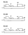
- FIG. 3 shows in (a) to (c) three further variants for the suppression of laser scattered light in a simplified representation.
- the glass prism 38A is provided with an absorbing layer 44A instead of a mirror 44.
- the glass prism 38B is implemented as a 45 ° mirror whose mirror surface 44B reflects laser scattering light upwardly.
- the surface 44B may be formed as a standard mirror with a metallic or dielectric coating, or be provided with an absorbent coating.
- Fig. 3 (c) shows a modification of the design of Fig. 3 (b), in which the 45 ° mirror surface 44C of the glass primate 38C is directed downwards, thus deflecting laser scattered light into the substrate where it is absorbed.
- the surface 44C may be both mirrored and provided with an absorbent layer.
- the silicon substrate 12 thus serves, in addition to its function as a support, thereon arranged glass prisms 36, 38, the laser diode 30 and the IC 42 also as a heat sink and as a substrate for a PIN photodiode array, which comprises the monitor photodiodes 18 and the signal diodes 20 and 22.
- the monitor photodiodes 18 are arranged in the vicinity of the laser diode 30 and measure the back reflection of one of the optical components for regulating the laser power.
- FIGS. 4 and 5 Another embodiment of a silicon submount 50 according to the invention is shown in FIGS. 4 and 5.
- the silicon submount 50 differs from the silicon submount 10 in particular by the arrangement of the monitor photodiode 52.
- the monitor photodiode 52 is arranged in this embodiment below the deflection prism 36. It takes as a monitor signal that part 54 of the laser radiation 32, which is transmitted through the mirrored surface of the deflection prism and refracted to the monitor diode 52 out.
- FIG. 5 embodies the variant shown in FIG. 3 (c) as means for reducing the stray light, in which the support element 38C is designed as a deflection element with a mirror surface 44C inclined at 45 ° to the substrate 12.
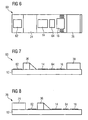
- Figures 6 and 7 show another embodiment of a silicon submount 60 according to the invention. Again, like reference numerals designate the same elements as in the silicon submount 10 of Figs. 1 and 2.
- a single signal detector 62 instead of the pair of signal detectors 20 and 22 of Fig. 1, a single signal detector 62 performs all functions for tracking, measurement the signal level and focus.
- the monitor diode 64 is arranged in the direction opposite to the emission direction of the laser, directly behind the first chip bonding surface 14.
- FIG. 8 shows a modification of the design of FIG. 7, in which the second support element 74 is bonded in the emission direction behind the single signal detector 62 to the substrate 12. The arrangement of the remaining elements corresponds to that of FIG. 7.
- FIGS. 9 and 10 Another embodiment of the invention is shown in FIGS. 9 and 10.
- a further glass support point is dispensed with in addition to the glass bonding surface 82 which serves to receive the deflection prism 84.
- the deflection prism 84 thus represents the only support element for the optical component 40.
- the arrangement and design of the signal diodes 20, 22 corresponds in the embodiment shown in FIG. 1, the arrangement and design of the monitor diode 64 of FIG .. 6
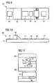
- FIG. 1 Another embodiment of the invention is shown in FIG.
- the support elements 38D, 38E are arranged laterally of the deflection mirror 36 and the detectors 20, 22 are installed between the mirror 36 and the support elements 38D, 38E.
- the optical element 40 is mounted on the support elements.
- FIG. 12 shows in (a) to (d) four variants for the implementation of a signal detector array 90, 92, 94 or 96.
- Each of these arrays allows a good measurement of track, distance and signal level of the reflected laser light and can be used for one of the signal detectors 20, 22 and 62 of the above-discussed silicon submounts are used.
- the production of the submounts takes place in the wafer assembly, for example on 150 mm or 200 mm disks, wherein for example 1500 submounts can be arranged on a 150 mm wafer.
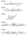
- FIG. 13 (a) 100 areas 102 are metallized on a glass wafer, which later serve as soldering surfaces for connecting the optical component 40. Then, about 20 microns deep trenches 104 are introduced by sand blasting on the back of the glass wafer 100. Subsequently, the glass wafer 100 is sawn to form a plurality of individual strips 106, Fig. 13 (b).
- Fig. 13 (c) 45 ° surfaces 108 are ground together on a plurality of the stiffeners 106. These surfaces 108 are polished in the next operation and coated with a highly reflective mirror for the laser beam deflection. Subsequently, the prisms are oriented on an silicon wafer 110 and anodically bonded, Fig. 13 (d).
- the Glasffenstoffteil is respectively separated out, so that from each glass strip 106, a deflection prism 36 and another support member 38 is formed. Also, the individual submounts 112 are separated from each other, Fig. 13 (e). The submounts 112 are initially held on a slide and then set by pick & place in a conventional manner in readhead housing.
Landscapes
- Physics & Mathematics (AREA)
- Optics & Photonics (AREA)
- Optical Head (AREA)
- Semiconductor Lasers (AREA)
Abstract
Claims (20)
- Tête d'analyse optique pour extraire une mémoire d'informations optique, comprenant- un substrat (12) ayant une surface principale,- un composant (30) laser disposé sur la surface principale du substrat (12), émettant par le bord et dont l'axe (34) d'émission est pour l'essentiel parallèle au premier plan principal,- un dispositif (36) de déviation disposé sur la surface principale du substrat pour dévier le rayonnement (32) laser dans une direction pour l'essentiel perpendiculaire à la surface principale,- au moins un détecteur (20, 22 ; 62) de signal pour détecter le rayonnement laser réfléchi par la mémoire d'informations optique, et- un élément (40) optique qui guide le rayonnement laser dévié vers la mémoire d'informations optique et le rayonnement laser réfléchi vers le au moins un détecteur (20, 22) de signal,dans laquelle l'élément (40) optique est relié au substrat (12) par au moins un élément (36, 38) d'appui,
caractérisée en ce que
le au moins un élément (36, 38) d'appui et/ou le dispositif (36) de déviation sont fabrigués de verre et le au moins un élément (36, 38) d'appui et/ou le dispositif (36) de déviation sont reliés au substrat d'une manière fixe par des liaisons anodiques. - Tête d'analyse optique suivant la revendication 1,
caractérisée en ce que
le dispositif (36) de déviation est constitué en même temps en élément d'appui par lequel l'élément (40) optique est relié au substrat (12). - Tête d'analyse optique suivant la revendication 1 ou 2,
caractérisée
en ce qu'un détecteur (20 ; 62) de signal de sens d'émission est disposé sur la surface principale du substrat (12) sur l'axe (34) d'émission du composant (30) laser et dans la direction (32) d'émission derrière le dispositif (36) de déviation. - Tête d'analyse optique suivant l'une des revendications précédentes,
caractérisée en ce
qu'un détecteur (22) de signal de sens opposé est disposé sur la surface principale du substrat (12) sur l'axe (34) d'émission du composant (30) laser et en sens opposé à la direction (32) d'émission. - Tête d'analyse optique suivant la revendication 4,
caractérisée en ce
qu'il est interposé entre le composant (30) laser et le détecteur (22) de signal de sens opposé un élément (38) d'appui par lequel l'élément (40) optique est relié au substrat (12). - Tête d'analyse optique suivant la revendication 5,
caractérisée en ce que
l'élément (38) d'appui disposé entre le composant (30) laser et le détecteur (22) de signal de sens opposé est muni, sur sa surface tournée vers le composant laser, d'une couche (44) de miroir métallique ou diélectrique. - Tête d'analyse optique suivant la revendication 5,
caractérisée en ce que
l'élément (38A) d'appui disposé entre le composant (30) laser et le détecteur (22) de signal de sens opposé est muni, sur sa surface tournée vers le composant laser, d'une couche (44A) d'absorption. - Tête d'analyse optique suivant l'une des revendications 5 à 7,
caractérisée en ce que
l'élément d'appui disposé entre le composant (30) laser et le détecteur (22) de signal opposé est constitué en dispositif (38B, 38C) de déviation, qui détourne la lumière diffusée du composant (30) laser du détecteur (22) de signal de sens opposé. - Tête d'analyse optique suivant la revendication 8,
caractérisée en ce que
l'élément d'appui constitué en dispositif (38B, 38C) de déviation dévie de la lumière diffusée dans une direction pour l'essentiel perpendiculaire à la surface principale. - Tête d'analyse optique suivant l'une des revendications précédentes,
caractérisée en ce que
le au moins un détecteur (20, 22 ; 62) de signal est formé dans le substrat (12). - Tête d'analyse optique suivant la revendication 10,
caractérisée en ce que
le au moins un détecteur (20, 22 ; 62) de signal comprend un réseau (90 ; 92 ; 94 ; 96) de photodiodes PIN formées dans le substrat (12). - Tête d'analyse optique suivant l'une des revendications précédentes,
caractérisée en ce
qu'un détecteur (18 ; 52; 64) de moniteur est intégré sur le substrat (12) pour le contrôle de la puissance émise par le composant (30) laser. - Tête d'analyse optique suivant l'une des revendications précédentes,
caractérisée en ce que
les éléments (38D, 38E) d'appui sont disposés latéralement au miroir (36) de déviation, les détecteurs (20, 22) sont montés entre le miroir (36) et les éléments (38D, 38E) d'appui et l'élément (40) optique est fixé sur les éléments (38D, 38E) d'appui. - Tête d'analyse optique suivant l'une des revendications précédentes,
caractérisée en ce que
le substrat (12) est formé d'un substrat en silicium. - Tête d'analyse optique suivant l'une des revendications précédentes,
caractérisée en ce que
la surface principale du substrat (12) a une superficie inférieure ou égale à 10 mm2. - Procédé de production d'une tête d'analyse optique suivant l'une des revendication 1 à 15, dans lequel, pour la production du dispositif de déviation- on scie une plaquette de verre en bandes individuelles,- on taille sur les bandes des surfaces sous un angle déterminé à l'avance, notamment sous un angle d'environ 45°,- on recouvre les surfaces taillées d'une couche de miroir très réfléchissante pour obtenir un prisme de déviation du faisceau laser, et- on oriente les prismes de déviation et on les relie de manière fixe avec le substrat,caractérisé en ce que l'on relie les prismes de déviation au substrat par des liaisons anodiques.
- Procédé suivant la revendication 16,
caractérisé en ce que
avant de scier la plaquette de verre, on métallise des parties sur la face avant de la plaquette de verre pour ménager des surfaces de métallisation pour la fixation de composants optiques après la liaison des prismes des déviations avec le substrat. - Procédé suivant la revendication 16 ou 17,
caractérisé en ce que
avant de scier la plaquette de verre on ménage par sablage des sillons dans la face arrière de la plaquette de verre. - Procédé suivant l'une des revendications 16 à 18,
caractérisé en ce que
l'on produit les éléments d'appui en même temps que le dispositif de déviation de la plaquette de verre. - Procédé suivant l'une des revendications 16 à 19,
caractérisé en ce que
l'on forme comme détecteur(s) de signal un réseau de photodiodes PIN dans le substrat.
Applications Claiming Priority (5)
| Application Number | Priority Date | Filing Date | Title |
|---|---|---|---|
| DE10243756 | 2002-09-20 | ||
| DE10243756 | 2002-09-20 | ||
| DE10253907A DE10253907A1 (de) | 2002-09-20 | 2002-11-19 | Optischer Abtastkopf und Verfahren zur Herstellung desselben |
| DE10253907 | 2002-11-19 | ||
| PCT/DE2003/002542 WO2004029948A1 (fr) | 2002-09-20 | 2003-07-29 | Tete de balayage optique et son procede de production |
Publications (2)
| Publication Number | Publication Date |
|---|---|
| EP1540649A1 EP1540649A1 (fr) | 2005-06-15 |
| EP1540649B1 true EP1540649B1 (fr) | 2007-09-12 |
Family
ID=32043950
Family Applications (1)
| Application Number | Title | Priority Date | Filing Date |
|---|---|---|---|
| EP03798045A Expired - Lifetime EP1540649B1 (fr) | 2002-09-20 | 2003-07-29 | Tete de balayage optique et son procede de production |
Country Status (6)
| Country | Link |
|---|---|
| EP (1) | EP1540649B1 (fr) |
| JP (1) | JP2005539344A (fr) |
| KR (1) | KR20050057448A (fr) |
| DE (1) | DE50308190D1 (fr) |
| TW (1) | TWI237253B (fr) |
| WO (1) | WO2004029948A1 (fr) |
Families Citing this family (1)
| Publication number | Priority date | Publication date | Assignee | Title |
|---|---|---|---|---|
| TWI320783B (en) | 2005-04-14 | 2010-02-21 | Otsuka Pharma Co Ltd | Heterocyclic compound |
Family Cites Families (4)
| Publication number | Priority date | Publication date | Assignee | Title |
|---|---|---|---|---|
| CA2088701C (fr) * | 1992-02-05 | 1998-01-27 | Yoshio Yoshida | Appareil de lecture optique d'informations |
| US5689108A (en) * | 1995-05-27 | 1997-11-18 | Victor Company Of Japan, Ltd. | Integrated optical pick-up |
| US5912872A (en) * | 1996-09-27 | 1999-06-15 | Digital Optics Corporation | Integrated optical apparatus providing separated beams on a detector and associated methods |
| US6385157B1 (en) * | 2000-12-11 | 2002-05-07 | Olympus Optical Co., Ltd. | Optical pick-up device |
-
2003
- 2003-07-29 EP EP03798045A patent/EP1540649B1/fr not_active Expired - Lifetime
- 2003-07-29 JP JP2004538684A patent/JP2005539344A/ja active Pending
- 2003-07-29 KR KR1020057004680A patent/KR20050057448A/ko not_active Ceased
- 2003-07-29 DE DE50308190T patent/DE50308190D1/de not_active Expired - Lifetime
- 2003-07-29 WO PCT/DE2003/002542 patent/WO2004029948A1/fr not_active Ceased
- 2003-09-02 TW TW092124195A patent/TWI237253B/zh not_active IP Right Cessation
Also Published As
| Publication number | Publication date |
|---|---|
| EP1540649A1 (fr) | 2005-06-15 |
| KR20050057448A (ko) | 2005-06-16 |
| TW200405318A (en) | 2004-04-01 |
| JP2005539344A (ja) | 2005-12-22 |
| WO2004029948A1 (fr) | 2004-04-08 |
| DE50308190D1 (de) | 2007-10-25 |
| TWI237253B (en) | 2005-08-01 |
Similar Documents
| Publication | Publication Date | Title |
|---|---|---|
| EP0664585B1 (fr) | Module de transmission et de réception pour système de communication bidirectionnel | |
| EP0660467B1 (fr) | Elément optoélectronique et sa méthode de fabrication | |
| DE69705848T2 (de) | Verfahren zum erzielen von mehreren integrierten optischen köpfe | |
| DE69906704T2 (de) | Integriertes optisches gerät zur erzeugung von getrennten strahlen auf einem detektor, und zugehörige verfahren | |
| EP0631163B1 (fr) | Emetteur-récepteur optique bidirectionnel | |
| DE19640423C1 (de) | Optoelektronisches Modul zur bidirektionalen optischen Datenübertragung | |
| DE3833096C2 (fr) | ||
| DE19621124A1 (de) | Optoelektronischer Wandler und dessen Herstellungsverfahren | |
| DE69419550T2 (de) | Optischer Kopf | |
| DE3887026T2 (de) | Optischer Wandler. | |
| EP0713113A1 (fr) | Dispositif optique émetteur et récepteur | |
| DE4440976A1 (de) | Optische Sende- und Empfangseinrichtung mit einem oberflächenemittierenden Laser | |
| DE10201102A1 (de) | Laservorrichtung | |
| DE10253907A1 (de) | Optischer Abtastkopf und Verfahren zur Herstellung desselben | |
| DE19748324C2 (de) | Optoelektronisches Sensormodul | |
| EP1540649B1 (fr) | Tete de balayage optique et son procede de production | |
| EP0790678A2 (fr) | Dispositif de raccordement optique d'une diode de contrÔle à une diode laser | |
| DE4313492C1 (de) | Anordnung zur Ankopplung eines optoelektronischen Empfangselementes an ein optoelektronisches Sendeelement | |
| DE19640421A1 (de) | Optoelektronisches Modul zur bidirektionalen optischen Datenübertragung | |
| EP1597774B1 (fr) | Composant optoélectronique comportant une diode luminescente et une pluralité de capteurs de lumière | |
| WO1997025638A2 (fr) | Dispositif pour le couplage optique d'un element photo-emetteur avec un element photorecepteur | |
| EP0942302A2 (fr) | Module électrooptique | |
| DE19718949A1 (de) | Elektrooptisches Modul | |
| EP1568158B1 (fr) | Module d'emission et de reception bidirectionnel | |
| EP1146570A1 (fr) | Dispositif émetteur de lumière à semi-conducteur et methode pour la fabrication d'un support |
Legal Events
| Date | Code | Title | Description |
|---|---|---|---|
| PUAI | Public reference made under article 153(3) epc to a published international application that has entered the european phase |
Free format text: ORIGINAL CODE: 0009012 |
|
| 17P | Request for examination filed |
Effective date: 20050113 |
|
| AK | Designated contracting states |
Kind code of ref document: A1 Designated state(s): AT BE BG CH CY CZ DE DK EE ES FI FR GB GR HU IE IT LI LU MC NL PT RO SE SI SK TR |
|
| 17Q | First examination report despatched |
Effective date: 20050630 |
|
| RBV | Designated contracting states (corrected) |
Designated state(s): DE FR |
|
| 17Q | First examination report despatched |
Effective date: 20050630 |
|
| RIN1 | Information on inventor provided before grant (corrected) |
Inventor name: SINGER, FRANK Inventor name: KAEMPF, MATHIAS Inventor name: GRAMANN, WOLFGANG Inventor name: DACHS, JUERGEN Inventor name: STEEGMUELLER, ULRICH |
|
| GRAP | Despatch of communication of intention to grant a patent |
Free format text: ORIGINAL CODE: EPIDOSNIGR1 |
|
| GRAS | Grant fee paid |
Free format text: ORIGINAL CODE: EPIDOSNIGR3 |
|
| GRAA | (expected) grant |
Free format text: ORIGINAL CODE: 0009210 |
|
| AK | Designated contracting states |
Kind code of ref document: B1 Designated state(s): DE FR |
|
| REF | Corresponds to: |
Ref document number: 50308190 Country of ref document: DE Date of ref document: 20071025 Kind code of ref document: P |
|
| RAP2 | Party data changed (patent owner data changed or rights of a patent transferred) |
Owner name: OSRAM OPTO SEMICONDUCTORS GMBH |
|
| RAP2 | Party data changed (patent owner data changed or rights of a patent transferred) |
Owner name: OSRAM OPTO SEMICONDUCTORS GMBH |
|
| ET | Fr: translation filed | ||
| PLBE | No opposition filed within time limit |
Free format text: ORIGINAL CODE: 0009261 |
|
| STAA | Information on the status of an ep patent application or granted ep patent |
Free format text: STATUS: NO OPPOSITION FILED WITHIN TIME LIMIT |
|
| 26N | No opposition filed |
Effective date: 20080613 |
|
| PGFP | Annual fee paid to national office [announced via postgrant information from national office to epo] |
Ref country code: FR Payment date: 20140721 Year of fee payment: 12 |
|
| REG | Reference to a national code |
Ref country code: FR Ref legal event code: ST Effective date: 20160331 |
|
| PG25 | Lapsed in a contracting state [announced via postgrant information from national office to epo] |
Ref country code: FR Free format text: LAPSE BECAUSE OF NON-PAYMENT OF DUE FEES Effective date: 20150731 |
|
| PGFP | Annual fee paid to national office [announced via postgrant information from national office to epo] |
Ref country code: DE Payment date: 20180723 Year of fee payment: 16 |
|
| REG | Reference to a national code |
Ref country code: DE Ref legal event code: R119 Ref document number: 50308190 Country of ref document: DE |
|
| PG25 | Lapsed in a contracting state [announced via postgrant information from national office to epo] |
Ref country code: DE Free format text: LAPSE BECAUSE OF NON-PAYMENT OF DUE FEES Effective date: 20200201 |