EP1538481A1 - Methode zur Aktivierung einer Silizium-Oberfläche im Hinblick auf die Erzeugung von Mustern auf dieser Oberfläche - Google Patents
Methode zur Aktivierung einer Silizium-Oberfläche im Hinblick auf die Erzeugung von Mustern auf dieser Oberfläche Download PDFInfo
- Publication number
- EP1538481A1 EP1538481A1 EP03028132A EP03028132A EP1538481A1 EP 1538481 A1 EP1538481 A1 EP 1538481A1 EP 03028132 A EP03028132 A EP 03028132A EP 03028132 A EP03028132 A EP 03028132A EP 1538481 A1 EP1538481 A1 EP 1538481A1
- Authority
- EP
- European Patent Office
- Prior art keywords
- silicon surface
- molecules
- stamp
- cyanuric chloride
- ink
- Prior art date
- Legal status (The legal status is an assumption and is not a legal conclusion. Google has not performed a legal analysis and makes no representation as to the accuracy of the status listed.)
- Withdrawn
Links
Images


Classifications
-
- G—PHYSICS
- G03—PHOTOGRAPHY; CINEMATOGRAPHY; ANALOGOUS TECHNIQUES USING WAVES OTHER THAN OPTICAL WAVES; ELECTROGRAPHY; HOLOGRAPHY
- G03F—PHOTOMECHANICAL PRODUCTION OF TEXTURED OR PATTERNED SURFACES, e.g. FOR PRINTING, FOR PROCESSING OF SEMICONDUCTOR DEVICES; MATERIALS THEREFOR; ORIGINALS THEREFOR; APPARATUS SPECIALLY ADAPTED THEREFOR
- G03F7/00—Photomechanical, e.g. photolithographic, production of textured or patterned surfaces, e.g. printing surfaces; Materials therefor, e.g. comprising photoresists; Apparatus specially adapted therefor
- G03F7/26—Processing photosensitive materials; Apparatus therefor
-
- H—ELECTRICITY
- H01—ELECTRIC ELEMENTS
- H01L—SEMICONDUCTOR DEVICES NOT COVERED BY CLASS H10
- H01L21/00—Processes or apparatus adapted for the manufacture or treatment of semiconductor or solid state devices or of parts thereof
- H01L21/02—Manufacture or treatment of semiconductor devices or of parts thereof
- H01L21/02041—Cleaning
- H01L21/02043—Cleaning before device manufacture, i.e. Begin-Of-Line process
- H01L21/02054—Cleaning before device manufacture, i.e. Begin-Of-Line process combining dry and wet cleaning steps
-
- B—PERFORMING OPERATIONS; TRANSPORTING
- B82—NANOTECHNOLOGY
- B82Y—SPECIFIC USES OR APPLICATIONS OF NANOSTRUCTURES; MEASUREMENT OR ANALYSIS OF NANOSTRUCTURES; MANUFACTURE OR TREATMENT OF NANOSTRUCTURES
- B82Y10/00—Nanotechnology for information processing, storage or transmission, e.g. quantum computing or single electron logic
-
- B—PERFORMING OPERATIONS; TRANSPORTING
- B82—NANOTECHNOLOGY
- B82Y—SPECIFIC USES OR APPLICATIONS OF NANOSTRUCTURES; MEASUREMENT OR ANALYSIS OF NANOSTRUCTURES; MANUFACTURE OR TREATMENT OF NANOSTRUCTURES
- B82Y40/00—Manufacture or treatment of nanostructures
-
- C—CHEMISTRY; METALLURGY
- C07—ORGANIC CHEMISTRY
- C07H—SUGARS; DERIVATIVES THEREOF; NUCLEOSIDES; NUCLEOTIDES; NUCLEIC ACIDS
- C07H21/00—Compounds containing two or more mononucleotide units having separate phosphate or polyphosphate groups linked by saccharide radicals of nucleoside groups, e.g. nucleic acids
-
- G—PHYSICS
- G03—PHOTOGRAPHY; CINEMATOGRAPHY; ANALOGOUS TECHNIQUES USING WAVES OTHER THAN OPTICAL WAVES; ELECTROGRAPHY; HOLOGRAPHY
- G03F—PHOTOMECHANICAL PRODUCTION OF TEXTURED OR PATTERNED SURFACES, e.g. FOR PRINTING, FOR PROCESSING OF SEMICONDUCTOR DEVICES; MATERIALS THEREFOR; ORIGINALS THEREFOR; APPARATUS SPECIALLY ADAPTED THEREFOR
- G03F7/00—Photomechanical, e.g. photolithographic, production of textured or patterned surfaces, e.g. printing surfaces; Materials therefor, e.g. comprising photoresists; Apparatus specially adapted therefor
- G03F7/0002—Lithographic processes using patterning methods other than those involving the exposure to radiation, e.g. by stamping
-
- H—ELECTRICITY
- H01—ELECTRIC ELEMENTS
- H01L—SEMICONDUCTOR DEVICES NOT COVERED BY CLASS H10
- H01L21/00—Processes or apparatus adapted for the manufacture or treatment of semiconductor or solid state devices or of parts thereof
- H01L21/02—Manufacture or treatment of semiconductor devices or of parts thereof
- H01L21/04—Manufacture or treatment of semiconductor devices or of parts thereof the devices having at least one potential-jump barrier or surface barrier, e.g. PN junction, depletion layer or carrier concentration layer
- H01L21/18—Manufacture or treatment of semiconductor devices or of parts thereof the devices having at least one potential-jump barrier or surface barrier, e.g. PN junction, depletion layer or carrier concentration layer the devices having semiconductor bodies comprising elements of Group IV of the Periodic System or AIIIBV compounds with or without impurities, e.g. doping materials
- H01L21/30—Treatment of semiconductor bodies using processes or apparatus not provided for in groups H01L21/20 - H01L21/26
- H01L21/302—Treatment of semiconductor bodies using processes or apparatus not provided for in groups H01L21/20 - H01L21/26 to change their surface-physical characteristics or shape, e.g. etching, polishing, cutting
- H01L21/306—Chemical or electrical treatment, e.g. electrolytic etching
-
- Y—GENERAL TAGGING OF NEW TECHNOLOGICAL DEVELOPMENTS; GENERAL TAGGING OF CROSS-SECTIONAL TECHNOLOGIES SPANNING OVER SEVERAL SECTIONS OF THE IPC; TECHNICAL SUBJECTS COVERED BY FORMER USPC CROSS-REFERENCE ART COLLECTIONS [XRACs] AND DIGESTS
- Y10—TECHNICAL SUBJECTS COVERED BY FORMER USPC
- Y10T—TECHNICAL SUBJECTS COVERED BY FORMER US CLASSIFICATION
- Y10T428/00—Stock material or miscellaneous articles
- Y10T428/24—Structurally defined web or sheet [e.g., overall dimension, etc.]
- Y10T428/24802—Discontinuous or differential coating, impregnation or bond [e.g., artwork, printing, retouched photograph, etc.]
Definitions
- the present invention relates to a method of activating a silicon surface for subsequent patterning of molecules onto said surface, and to patterns produced by this method, and further to uses of said pattern.
- Patterning in particular Microcontact printing ( ⁇ CP).
- soft lithography there are six techniques normally referred to as soft lithography: microtransfer molding, replica molding, micromolding in capillaries, solvent-assisted microcontact molding, near field phase shifted lithography and microcontact printing (also often abbreviated as ⁇ CP).
- ⁇ CP a liquid polymer precursor (usually polydimethylsiloxane, PDMS) is poured over a master that has been produced by photo- or electron beam lithography. After curing, the PDMS stamp with the desired pattern is peeled off the master (Xia and Whitesides, 1998, Annu. Rev. Mater. Sci. 28, 153).
- inking the stamp there are two possible methods of inking the stamp (Michel et al ., 2001, IBM J. Res. & Dev. 5, 697): immersion inking and contact inking.
- immersion inking the stamp is inked with a solution and subsequently dried.
- contact inking the stamp is simply pressed on an inkpad, which is usually a block of PDMS that was previously treated with the ink solution. Subsequent pressing of the inked stamp on a substrate transfers the molecules contained in the ink from the stamp to the substrate.
- the elasticity of the stamp is one of the parameters that determine the resolution limits of the soft-lithography (Michel et al ., 2001, see above).
- Commercial PDMS with a Young's modulus of 3 MPa, is too soft to define structures smaller than 500 nm.
- the hardness of the polymer can be changed by varying the ratio of pre-polymer to cross-linker and therefore the molecular mass M C between the cross-links or by mixing different types of polymer precursors (Schmid and Michel, 2000, Macromolecules 33, 3042).
- stamp materials with a Young's modulus of 9.7 MPa and sufficient toughness for large area printing can be made.
- step b) is performed by exposing said silicon surface resulting from a) to cyanuric chloride, preferably to a solution of cyanuric chloride.
- said silicon surface resulting from step b) is exposed to cyanuric chloride, over its entire area or at least over a substantial part of its area involving also regions not intended to be covered by said molecules to be patterned, wherein, preferably, exposing said surface to cyanuric chloride occurs by immersion of said silicon surface into a solution of cyanuric chloride or by dripping or depositing a solution of cyanuric chloride onto said surface.
- steps c) and d) are performed by
- step b) is performed by
- said inked stamp is withdrawn from said silicon surface.
- steps c) and d) are performed by exposing said silicon surface to said molecules to be patterned, preferably to a solution of said molecules, wherein, preferably, said silicon surface is exposed to said molecules to be patterned, over its area entire area or at least over a substantial part of its area involving also regions not intended to be covered by said molecules to be patterned.
- exposing said silicon surface to said molecules to be patterned occurs by immersion of said silicon surface into a composition, preferably a solution, of said molecules, or by dripping or depositing said molecules onto said surface.
- step b) occurs in the presence of a base.
- said molecules to be patterned are molecules containing nucleophilic groups, preferably with active hydrogen atoms, wherein, more preferably, said molecules containing nucleophilic groups are in solution and at a concentration in the range of 1 ⁇ M - 100 mM.
- said molecules containing nucleophilic groups are selected from the group comprising ammonia, primary amines, secondary amines, water, alcohols, phenols, thiols and mercaptans.
- said immersion inking is achieved by immersing said stamp into said ink or by placing said ink onto said stamp.
- said contact inking is achieved by placing said stamp on an ink pad that has previously been treated with said ink, or by placing an ink pad that has previously been treated with said ink onto said stamp.
- said stamp is made of an elastic material having a Young's modulus in the range of 1 MPa to 50 MPa, preferably 1 MPa to 20 MPa, more preferably 2 MPa to 15 MPa.
- the method according to the present invention comprises the additional steps:
- said silicon surface used for a) has been pre-patterned with gold electrode structures.
- said silicon surface has a (100) or (110) or (111) surface orientation, wherein, more preferably, said silicon surface has a native or thermally grown oxide layer on it.
- said silicon surface is part of a silicon substrate that is doped (n-type or p-type) or undoped.
- said treatment of said silicon surface with HF is done by treating said silicon surface with aqueous HF that may contain HCl, wherein, preferably, said aqueous HF has a concentration that lies in the range of 0.06 M to 6 M, preferably approximately 0.6 M, and said HCl has a concentration that lies in the range of 0.01 to 10 M, preferably 0.01 M to 1 M.
- said treatment with aqueous HF occurs for 0.1 - 10 minutes, preferably at 0°C to 90°C, more preferably 10°C to 40°C.
- a treatment with aqueous HF is performed if said silicon surface has a (100) or (110) surface orientation.
- said treatment of said silicon surface with HF is done by treating said silicon surface with aqueous NH 4 F that may contain NH 4 OH, wherein, preferably, said aqueous NH 4 F has a concentration that lies in the range of 0.1 - 11 M, preferably approximately 2 M, and said NH 4 OH has a concentration that lies in the range of 0.01 M to 10 M.
- said treatment with aqueous NH 4 F occurs for 0.1 - 10 min, preferably at 0°C to 90°C, more preferably 10°C to 40°C.
- a treatment with aqueous NH 4 F is performed if said silicon surface has a (111) surface orientation.
- said treatment with cyanuric chloride (step b)) is performed using a solution of cyanuric chloride, preferably having a concentration in the range of from 0.1 - 10 wt.%, wherein, preferably, said treatment with cyanuric chloride is performed over 1 - 100 min, preferably at 0 - 50°C.
- said base is selected from the group comprising sterically hindered tertiary organic amines or phosphazene bases, preferably N-ethyldiisopropylamine, N,N-diisopropylisobutylamine, tributylamine, 2,2,6,6-tetramethylpiperidine, N,N,N',N'-tetramethyl-1,8-naphthalenediamine, 2,4,6-tri-tert-butylpyridine, tert-butylimino-tris-(dimethylamine)-phosphorane, or tert-butylimino-tri-pyrrolidino-phosphorane, wherein, preferably, said base has a concentration in the range of 0% to 10 wt.%.
- said molecules containing nucleophilic groups are selected from the group comprising ammonia,. primary amines, secondary amines, water, alcohols, phenols, thiols and mercaptans.
- the objects of the present invention are also solved by a pattern of molecules on a silicon surface produced by the method according to the present invention.
- the objects of the present invention are also solved by the use of the pattern according to the present invention in an electronic device, a memory device, a photonic device, an energy conversion device, a display device, a sensor device, a biochip, an actuator, an electromechanical device or a microfluidic device.
- the objects of the present invention are furthermore solved by the use of cyanuric chloride to activate a silicon surface for subsequent patterning of molecules onto said silicon surface, preferably by performing the method according to the present invention.
- the silicon surface to be activated by cyanuric chloride is H-terminated.
- an activated silicon surface produced by the use according to the present invention or produced by the method according to the present invention, wherein preferably the activated silicon surface, after activation by cyanuric chloride, is still H-terminated in a proportion of its surface area.
- the objects of the present invention are furthermore solved by an activated silicon surface, preferably as described in the previous sentence, to which 2,4-dichloro-triazine is covalently linked.
- an activated silicon surface for the fabrication of an electronic device, a memory device, a photonic device, an energy conversion device, a display device, a sensor device, a biochip, an actuator, an electromechanical device or a microfluidic device.
- microcontact printing is meant to designate any process useful for applying an ink onto a surface, preferably such that the dimensions of the printed structures lie in the ⁇ m-range, more preferably in the nm-range.
- microcontact printing as such is a process well known to someone skilled in the art.
- microcontact printing can also be used interchangeably with simply “printing”, albeit on a ⁇ m-scale or nm-scale.
- patterning as used herein, is sometimes used herein as a more general term. It is meant to designate any process by which a pattern of molecules can be generated on a surface. One way of achieving this is on a nm-to- ⁇ m-scale is microcontact printing.
- inert when used herein in connection with a solvent, is meant to indicate that the solvent is not likely to undergo a chemical reaction, in particular not any reaction with cyanuric chloride and/or a reaction with the silicon surface activated by cyanuric chloride.
- cyanuric chloride is meant to designate the compound 2,4,6-trichloro-triazine, wherein the nitrogen atoms are preferably distributed in a symmetric(s) manner, i.e. 2,4,6-trichloro-s-triazine or, interchangeably 2,4,6-trichloro-1,3,5-triazine.
- the process according to the present invention is easy and quick to perform and allows for the fabrication of patterns that are comparable to standard soft lithography techniques.
- the present invention provides a quick process for patterning, in particular microcontact printing of molecules under ambient conditions onto doped or undoped Si surfaces with a native or thermally grown oxide surface.
- the substrate is silicon, preferably Si(100) or Si(110) or Si(111), doped (n- or p-type) or undoped, with native or thermally-grown oxide layer on the surface.
- the process is described below. In one embodiment, it involves in the first step a treatment with a dilute HF solution in order to create a H-terminated surface (Step 1). In the second step the H-terminated surface is treated with cyanuric chloride, preferably a solution thereof, resulting in an activated Si surface (Step 2).
- Step 2 may be facilitated by addition of a base such as N-ethyldiisopropylamine.
- the activated substrate is subsequently used for the pattern transfer process from a stamp.
- a stamp any molecule containing a nucleophilic group, such as an amine, alcohol, or thiol, is suitable, preferably selected from the group comprising ammonia, primary amines, secondary amines, water, alcohols, phenols, thiols and mercaptans.
- the concentration of the ink is typically in the range 0.1-100 mM and either contact inking or solution inking can be used (Step 3).
- the pattern transfer step involves placement of the inked stamp on the substrate (Step 4).
- the stamp is fabricated from a siloxane elastomer (Sylgard 184, Dow Coming), the material is soft enough (Young's modulus of 3 MPa) to provide a good contact between the stamp and the substrate. If the stamp has a larger Young's modulus ( ⁇ 9-10 MPa) additional pressure may be needed in order to establish a sufficient contact between the substrate and the stamp. The required additional pressure depends on the size of the printed structures (Michel et al ., 2001, see above). The time necessary for the pattern transfer depends on the width of the transferred patterns, the molecular weight of the ink molecule, and the substrate/molecule interaction. Printing times are typically between 1 s and 100 s.
- the substrate is thoroughly rinsed with the solvent that was used for the ink in order to remove excess and non-specifically absorbed ink material from the substrate.
- nucleophilic groups preferably selected from the group comprising ammonia, primary amines, secondary amines, water, alcohols, phenols, thiols and mercaptans.
- Substrates Silicon substrates, preferably Si(100) or Si(110) or Si(111), doped (n- or p-type) or undoped, with native or thermally-grown oxide layer on surface.
- Step 2 and Step 3 It is further possible to pattern H-terminated Si surfaces by exchanging the order of Step 2 and Step 3.
- a solution of cyanuric chloride with or without base is used as the ink.
- the PDMS stamp may be chemically altered, causing a change of its Young's modulus.
- Such stamps may not be reusable, and the process parameters may have to be adjusted in such a way that the ink-induced changes in the stamp do not affect the pattern transfer process.
- the patterned substrate is subsequently rinsed thoroughly with an inert solvent. This process results in the patterned regions of activated surface, which can then be reacted with molecules containing nucleophilic groups. An example of this process is described below (Example 5).
- the function of cyanuric chloride is to activate hydrogen-terminated silicon surfaces toward reaction with nucleophilic reagents. While not wishing to be limited by theory, the mechanism of activation is likely to involve one or both of two processes shown in Figure 1. In one of these processes, the triazine nucleus of cyanuric chloride (in the form of the 2,4-dichloro-s-triazine moiety) remains attached to the silicon surface, with elimination of HCl ( Figure 1 A). In the other process, cyanuric chloride serves as a chlorinating agent, with elimination of the resulting triazine compound ( Figure 1 B). A base such as a tertiary organic amine may facilitate the first of these processes by neutralizing the HCl that is produced.
- the activated silicon surfaces may react with nucleophilic reagents with the release of chloride ( Figure 2).
- the nucleophilic reagent is a primary amine containing an additional functional group X, H 2 N-R-X, where R is a saturated or unsaturated hydrocarbon moiety.
- the dichlorotriazine-terminated silicon surface created in the first process ( Figure 1A) can react with the nucleophilic reagent to replace one or both chlorine atoms of the triazine nucleus, as shown in Figure 2A and B. The replacement of both chlorine atoms can be performed in two steps using different nucleophilic reagents ( Figure 2C).
- the chlorine-terminated silicon surface created in the second process can react with the nucleophilic reagent to form a bond directly between the silicon and the nucleophile ( Figure 2D).
- Groups having different functionalities e.g., positive or negative charge, redox activity, photoluminescence, etc.
- micro-chemical modification/functionalization of silicon are utilized in the present invention for microcontact printing/patterning on planar silicon substrates, but the inventors also recognize the utility of said processes for surface-chemical modification/functionalization of micro- and nano-structured forms of silicon.
- Micro-and nano-structured forms of silicon that can be processed in this manner include porous silicon, silicon nanoparticles and nanowires, and silicon tips for scanning probe microscopy. These materials are being developed for various biological, electronic, and optical applications, including photoluminescent biological markers, sensors, non-volatile floating gate memories, and optical interconnects.
- Surface-chemical modification/functionalization of silicon is required for many of these applications to provide stability and/or dynamic range and/or for integration with other materials and/or components.
- the processing represented in Figure 1 and Figure 2 provides a general means for accomplishing the necessary surface chemistry to those who are familiar with the art.
- a Si(100) substrate ( n -doped with native oxide surface) was treated in the O 2 -plasma etcher for 5 min at 0.3 mbar. Subsequently it was dipped for 1 min in a HF solution (HF:H 2 O 1:50) and dried with compressed air (Step 1). The substrate was treated for 10 min with a solution of cyanuric chloride (100 mg in 900 ⁇ l acetone) and subsequently washed with acetone and dried with compressed air (Step 2). The solution inking process was used for inking of the stamp (Step 3).
- a PDMS stamp Sylgard 184, Dow Coming
- the ink solution was prepared by diluting 10-fold a commercially available solution of the dendrimers (Starburst® (PAMAM) Dendrimer, Generation 4, 10 wt.% solution in methyl alcohol, calculated FW 14,215, from Aldrich Chemical Co., Product #41,244-9). Subsequently the stamp was placed on the modified silicon substrate for 10 min (Step 4). Afterwards the sample was thoroughly rinsed with methanol and dried with compressed air (Step 5).
- Figure 3 shows SEM images of the transferred pattern, which consists of an interdigitated electrode structure having gaps and electrodes with a width of 5 ⁇ m.
- Figure 3A shows the printed contact pads (1), the printed electrodes (2) and structures with rounded edges (3) that result from stamp material that adhered to the surface during the printing process. This unspecific adhesion takes place because the distances between the printed structures are too large.
- Figure 3B shows a magnification of the electrodes with the gaps (1) and the bars (2).
- Figure 4 shows a section analysis of an AFM image of the printed structure. The height on the edge of the printed structure is ⁇ 4 nm, while the average height in the center of the structure is ⁇ 1.5 nm. The theoretical diameter of the dendrimer is about 4.5 nm.
- a Si(100) substrate (n-doped with native oxide surface) was treated in the O 2 -plasma etcher for 5 min at 0.3 mbar. Subsequently it was dipped for 1 min in a HF solution (HF:H 2 O 1:50) and dried with compressed air (Step 1). The substrate was treated for 10 min with a solution of cyanuric chloride and N-ethyldiisopropylamine in acetone (100 mg cyanuric chloride, 100 ⁇ l N-ethyldiisopropylamine in 800 ⁇ l acetone) and subsequently washed with acetone and dried with compressed air (Step 2). The solution inking process was used for inking of the stamp (Step 3).
- a PDMS stamp (Sylgard 184, Dow Coming) was placed for 10 min into an amine-terminated dendrimer ink solution and dried with compressed air.
- the ink solution was prepared by diluting 10-fold a commercially available solution of the dendrimers (Starburst® (PAMAM) Dendrimer, Generation 4, 10 wt.% solution in methyl alcohol, calculated FW 14,215, from Aldrich Chemical Co., Product #41,244-9).
- the stamp was placed on the modified silicon substrate for 10 min (Step 4). Afterwards the sample was thoroughly rinsed with methanol and dried with compressed air (Step 5).
- Figure 5 shows SEM images of the transferred pattern, which is the same as in Example 1.
- Figure 5A shows an SEM image of the transferred electrode bars.
- Figure 5B magnified view of Figure 5A
- the edges of the electrode bars are fuzzy. This is probably due to the presence of N-ethyldiisopropylamine in the ink, which may enhance the diffusion of the ink and also distort the PDMS stamp.
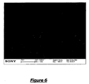
- a Si(100) substrate (n-doped with native oxide surface) was treated in the O 2 -plasma etcher for 5 min at 0.3 mbar. Subsequently it was dipped for 1 min in a HF solution (HF:H 2 O 1:50) and dried with compressed air (Step 1). The substrate was exposed for 10 min. to a solution of 100 mg cyanuric chloride and 900 ⁇ l acetone. Afterwards the substrate was thoroughly washed with acetone and dried with compressed air (Step 2). A PDMS stamp that was not inked was placed on the substrate for 10 min (Step 4). Afterwards the substrate was washed with methanol and dried with compressed air (Step 5). As can be seen from Figure 6, no pattern was transferred to the substrate.
- a nucleophilic reagent such as amine-terminated dendrimer is preferably used for developing the pattern.
- a Si(100) substrate ( n -doped with native oxide surface) was treated in the O 2 -plasma etcher for 5 min at 0.3 mbar. Subsequently it was dipped for 1 min in a HF solution (HF:H 2 O 1:50) and dried with compressed air (Step 1). The substrate was treated for 10 min with acetone and dried with compressed air.
- a PDMS stamp (Sylgard 184, Dow Coming) was placed for 10 min into an amine-terminated dendrimer ink solution and dried with compressed air.
- the ink solution was prepared by diluting 10-fold a commercially available solution of the dendrimers (Starburst® (PAMAM) Dendrimer, Generation 4, 10 wt.% solution in methyl alcohol, calculated FW 14,215, from Aldrich Chemical Co., Product #41,244-9). Subsequently the stamp was placed on the modified silicon substrate for 10 min (Step 4). Afterwards the substrate was washed with methanol and dried with compressed air (Step 5). As can be seen from Figure 7, no pattern was transferred to the substrate.
- This control experiment demonstrates that surface activation with cyanuric chloride is required for printing a nucleophilic reagent such as amine-terminated dendrimer.
- a Si(100) substrate ( n -doped with native oxide surface) was treated in the O 2 -plasma etcher for 5 min at 0.3 mbar. Subsequently it was dipped for 1 min in a HF solution (HF:H 2 O 1:50) and dried with compressed air (Step 1).
- a stamp was inked with a solution of cyanuric chloride and N-ethyldiisopropylamine in acetone (100 mg cyanuric chloride, 100 ⁇ l N-ethyldiisopropylamine in 800 ⁇ l acetone) and washed with acetone and dried with compressed air (Step 3).
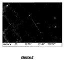
- the stamp was placed for 30 min on the substrate with a weight of 347 mg (Steps 2 and 4). After the pattern transfer process the substrate was washed with acetone. Subsequently the substrate was put into a solution of 4,7,10-trioxa-1,13-tridecanediamine (22 ⁇ l in 2 ml dichloromethane) for 30 min, in order to perform a nucleophilic substitution reaction on the patterned activated substrate. The substrate was washed with dichloromethane and dodecylamine stabilized Au-NPs were used for visualizing the amino functionalities of the transferred pattern.
- Figure 8 shows an SEM image of the Si-substrate.
- the transferred pattern which is a grid consisting of lines ⁇ 10 ⁇ m wide and ⁇ 100 ⁇ m long, is not perfect. The imperfections are partly due to the fact that the stamp was not perfect and the applied force during the printing process was too high.
- the PDMS in the stamp reacts with cyanuric chloride in the presence of the base N-ethyldiisopropylamine. Optimizing the inking time (Step 3) and the pattern transfer time (Step 4) are likely to lead to an improved pattern transfer.
- the process is also applicable to Si(110) or Si(111) substrates as well and insensitive to the nature of doping.
- the thickness of the oxide layer is not an important factor since the layer is removed in Step 1.
- Electrode structures (5 nm Cr and 50 nm Au) were prepared on a Si wafer with a 500 nm thermally grown SiO 2 layer.
- the substrates were cleaned with an O 2 plasma cleaner (Gala instruments) at an oxygen pressure of 0.4 mbar and 33W for 5 minutes. Subsequently the wafer was exposed for 1 min. to a 1% HF solution.
- the electrode structures remained unchanged, however, a slight, yet tolerable under etch was visible, meaning that this substrate can be used very well for subsequent activation through cyanuric chloride and the patterning process according to the present invention.
Priority Applications (5)
| Application Number | Priority Date | Filing Date | Title |
|---|---|---|---|
| EP03028132A EP1538481A1 (de) | 2003-12-05 | 2003-12-05 | Methode zur Aktivierung einer Silizium-Oberfläche im Hinblick auf die Erzeugung von Mustern auf dieser Oberfläche |
| KR1020040100927A KR20050054840A (ko) | 2003-12-05 | 2004-12-03 | 이어서 실리콘 표면에 분자를 패턴화시키기 위해 실리콘표면을 활성화시키는 방법 |
| US11/003,805 US7427477B2 (en) | 2003-12-05 | 2004-12-03 | Method of activating a silicon surface for subsequent patterning of molecules onto said surface |
| JP2004353303A JP2005244173A (ja) | 2003-12-05 | 2004-12-06 | シリコン表面の活性化方法、これにより生成される分子パターン及びその分子パターンの使用方法 |
| US12/173,490 US8092899B2 (en) | 2003-12-05 | 2008-07-15 | Method of activating a silicon surface for subsequent patterning of molecules onto said surface |
Applications Claiming Priority (1)
| Application Number | Priority Date | Filing Date | Title |
|---|---|---|---|
| EP03028132A EP1538481A1 (de) | 2003-12-05 | 2003-12-05 | Methode zur Aktivierung einer Silizium-Oberfläche im Hinblick auf die Erzeugung von Mustern auf dieser Oberfläche |
Publications (1)
| Publication Number | Publication Date |
|---|---|
| EP1538481A1 true EP1538481A1 (de) | 2005-06-08 |
Family
ID=34442978
Family Applications (1)
| Application Number | Title | Priority Date | Filing Date |
|---|---|---|---|
| EP03028132A Withdrawn EP1538481A1 (de) | 2003-12-05 | 2003-12-05 | Methode zur Aktivierung einer Silizium-Oberfläche im Hinblick auf die Erzeugung von Mustern auf dieser Oberfläche |
Country Status (4)
| Country | Link |
|---|---|
| US (2) | US7427477B2 (de) |
| EP (1) | EP1538481A1 (de) |
| JP (1) | JP2005244173A (de) |
| KR (1) | KR20050054840A (de) |
Cited By (3)
| Publication number | Priority date | Publication date | Assignee | Title |
|---|---|---|---|---|
| WO2008042079A2 (en) * | 2006-09-28 | 2008-04-10 | E. I. Du Pont De Nemours And Company | Method to form a pattern of functional material on a substrate |
| WO2017174755A1 (en) * | 2016-04-06 | 2017-10-12 | Koninklijke Philips N.V. | Imprint lithography stamp method of making and using the same |
| CN114454634A (zh) * | 2022-02-14 | 2022-05-10 | 中国科学院化学研究所 | 一种超高精度有机功能材料图案化的印刷制备方法及其应用 |
Families Citing this family (5)
| Publication number | Priority date | Publication date | Assignee | Title |
|---|---|---|---|---|
| JP4614330B2 (ja) * | 2005-01-31 | 2011-01-19 | 独立行政法人科学技術振興機構 | 有機基で修飾されたシリコン基板の製造方法 |
| WO2009042598A1 (en) * | 2007-09-25 | 2009-04-02 | Wilson-Cook Medical Inc. | Medical devices, systems, and methods for using tissue anchors |
| KR101724075B1 (ko) * | 2008-04-18 | 2017-04-06 | 메사추세츠 인스티튜트 오브 테크놀로지 | 불규칙한 표면의 웨지 임프린트 패터닝 |
| TWI508846B (zh) * | 2008-12-12 | 2015-11-21 | 麻省理工學院 | 不規則表面之楔形壓印圖案化 |
| ES2684851B2 (es) * | 2018-07-27 | 2019-06-19 | Univ Madrid Politecnica | Metodo para obtener puntas sensoras de microscopia de fuerza atomica funcionalizadas mediante silanizacion por vapor activado, y las puntas obtenidas por dicho metodo |
Citations (2)
| Publication number | Priority date | Publication date | Assignee | Title |
|---|---|---|---|---|
| US4716103A (en) * | 1983-08-09 | 1987-12-29 | Akademie Der Wissenschaften Der Ddr | Chemically active triazine support composition |
| US20030081463A1 (en) * | 2001-10-26 | 2003-05-01 | The Regents Of The University Of California | Formation of self-assembled monolayers of redox sams on silicon for molecular memory applications |
Family Cites Families (10)
| Publication number | Priority date | Publication date | Assignee | Title |
|---|---|---|---|---|
| JPS5565150A (en) * | 1978-11-10 | 1980-05-16 | Asahi Glass Co Ltd | Ion sensor |
| US6173720B1 (en) * | 1998-12-02 | 2001-01-16 | International Business Machines Corporation | Process for treating a semiconductor substrate |
| WO2000033976A1 (en) * | 1998-12-08 | 2000-06-15 | Gene Logic Inc. | Process for attaching organic molecules to silicon |
| US6413722B1 (en) * | 2000-03-22 | 2002-07-02 | Incyte Genomics, Inc. | Polymer coated surfaces for microarray applications |
| US6689858B2 (en) * | 2000-09-08 | 2004-02-10 | Wisconsin Alumni Research Foundation | Halogen-modified silicon, surfaces |
| US7172905B2 (en) * | 2001-08-07 | 2007-02-06 | The University Of Chicago | Polypeptide immobilization |
| US6802966B2 (en) * | 2001-08-14 | 2004-10-12 | W. R. Grace & Co. Conn. | Solid compositions for selective adsorption from complex mixtures |
| US7338613B2 (en) * | 2001-09-10 | 2008-03-04 | Surface Logix, Inc. | System and process for automated microcontact printing |
| IL152746A0 (en) * | 2002-11-11 | 2003-06-24 | Yissum Res Dev Co | Biosensor for molecules |
| US7259258B2 (en) * | 2003-12-17 | 2007-08-21 | Illumina, Inc. | Methods of attaching biological compounds to solid supports using triazine |
-
2003
- 2003-12-05 EP EP03028132A patent/EP1538481A1/de not_active Withdrawn
-
2004
- 2004-12-03 US US11/003,805 patent/US7427477B2/en not_active Expired - Fee Related
- 2004-12-03 KR KR1020040100927A patent/KR20050054840A/ko not_active Application Discontinuation
- 2004-12-06 JP JP2004353303A patent/JP2005244173A/ja active Pending
-
2008
- 2008-07-15 US US12/173,490 patent/US8092899B2/en not_active Expired - Fee Related
Patent Citations (2)
| Publication number | Priority date | Publication date | Assignee | Title |
|---|---|---|---|---|
| US4716103A (en) * | 1983-08-09 | 1987-12-29 | Akademie Der Wissenschaften Der Ddr | Chemically active triazine support composition |
| US20030081463A1 (en) * | 2001-10-26 | 2003-05-01 | The Regents Of The University Of California | Formation of self-assembled monolayers of redox sams on silicon for molecular memory applications |
Non-Patent Citations (1)
| Title |
|---|
| XIA Y ET AL: "SOFT LITHOGRAPHY", ANNUAL REVIEW OF MATERIALS SCIENCE, ANNUAL REVIEWS INC., PALO ALTO, CA, US, vol. 28, 1998, pages 153 - 184, XP009023786, ISSN: 0084-6600 * |
Cited By (9)
| Publication number | Priority date | Publication date | Assignee | Title |
|---|---|---|---|---|
| WO2008042079A2 (en) * | 2006-09-28 | 2008-04-10 | E. I. Du Pont De Nemours And Company | Method to form a pattern of functional material on a substrate |
| WO2008042079A3 (en) * | 2006-09-28 | 2008-05-22 | Du Pont | Method to form a pattern of functional material on a substrate |
| WO2017174755A1 (en) * | 2016-04-06 | 2017-10-12 | Koninklijke Philips N.V. | Imprint lithography stamp method of making and using the same |
| CN109313386A (zh) * | 2016-04-06 | 2019-02-05 | 皇家飞利浦有限公司 | 压印光刻印模的制作和使用方法 |
| RU2745059C2 (ru) * | 2016-04-06 | 2021-03-18 | Конинклейке Филипс Н.В. | Штамп для импринт-литографии и способ его изготовления и использования |
| US11163230B2 (en) | 2016-04-06 | 2021-11-02 | Koninklijke Philips N.V. | Imprint lithography stamp method of making and using the same |
| CN109313386B (zh) * | 2016-04-06 | 2022-06-28 | 皇家飞利浦有限公司 | 压印光刻印模的制作和使用方法 |
| US11860535B2 (en) | 2016-04-06 | 2024-01-02 | Koninklijke Philips N.V. | Imprint lithography stamp method of making and using the same |
| CN114454634A (zh) * | 2022-02-14 | 2022-05-10 | 中国科学院化学研究所 | 一种超高精度有机功能材料图案化的印刷制备方法及其应用 |
Also Published As
| Publication number | Publication date |
|---|---|
| US20050153074A1 (en) | 2005-07-14 |
| US7427477B2 (en) | 2008-09-23 |
| US20080280110A1 (en) | 2008-11-13 |
| US8092899B2 (en) | 2012-01-10 |
| KR20050054840A (ko) | 2005-06-10 |
| JP2005244173A (ja) | 2005-09-08 |
Similar Documents
| Publication | Publication Date | Title |
|---|---|---|
| US8092899B2 (en) | Method of activating a silicon surface for subsequent patterning of molecules onto said surface | |
| US11560009B2 (en) | Stamps including a self-assembled block copolymer material, and related methods | |
| US20050120902A1 (en) | Edge transfer lithography | |
| US20080038542A1 (en) | Method for high resolution patterning using soft X-ray, process for preparing nano device using the method | |
| US20020084429A1 (en) | Electron-beam patterning of functionalized self-assembled monolayers | |
| US8057857B2 (en) | Phase separation in patterned structures | |
| WO2000033976A1 (en) | Process for attaching organic molecules to silicon | |
| WO2001001199A1 (en) | Methods and materials for selective modification of photopatterned polymer films | |
| Heule et al. | Patterning colloidal suspensions by selective wetting of microcontact-printed surfaces | |
| US20070110639A1 (en) | System and method for positioning and synthesizing of nanostructures | |
| KR100473800B1 (ko) | 저에너지 전자빔을 이용하는 고정밀 패턴 형성 방법 | |
| Hinckley et al. | Detecting and removing defects in organosilane self-assembled monolayers | |
| US20110006035A1 (en) | Method for modifying surface in selective areas and method for forming patterns | |
| Pillers | Nanostructures as Dopant Sources: Maskless Nanoscale Patterning of Silicon Using Shape and Size Controlled Nanomaterials | |
| Zhang et al. | Micropatterning oligonucleotides on single-crystal diamond surface by photolithography | |
| Vogen | Inkless soft lithography: Utilizing immobilized enzymes and small molecules to pattern self-assembled monolayers via catalytic microcontact printing | |
| Chen | Investigation of modified polydimethylsiloxanes using chemical force microscopy. |
Legal Events
| Date | Code | Title | Description |
|---|---|---|---|
| PUAI | Public reference made under article 153(3) epc to a published international application that has entered the european phase |
Free format text: ORIGINAL CODE: 0009012 |
|
| AK | Designated contracting states |
Kind code of ref document: A1 Designated state(s): AT BE BG CH CY CZ DE DK EE ES FI FR GB GR HU IE IT LI LU MC NL PT RO SE SI SK TR |
|
| AX | Request for extension of the european patent |
Extension state: AL LT LV MK |
|
| RAP1 | Party data changed (applicant data changed or rights of an application transferred) |
Owner name: SONY DEUTSCHLAND GMBH |
|
| 17P | Request for examination filed |
Effective date: 20051122 |
|
| AKX | Designation fees paid |
Designated state(s): DE FR GB |
|
| RAP1 | Party data changed (applicant data changed or rights of an application transferred) |
Owner name: SONY DEUTSCHLAND GMBH |
|
| STAA | Information on the status of an ep patent application or granted ep patent |
Free format text: STATUS: THE APPLICATION IS DEEMED TO BE WITHDRAWN |
|
| 18D | Application deemed to be withdrawn |
Effective date: 20100701 |