EP1536515A1 - Dispositif d'antenne - Google Patents
Dispositif d'antenne Download PDFInfo
- Publication number
- EP1536515A1 EP1536515A1 EP04027521A EP04027521A EP1536515A1 EP 1536515 A1 EP1536515 A1 EP 1536515A1 EP 04027521 A EP04027521 A EP 04027521A EP 04027521 A EP04027521 A EP 04027521A EP 1536515 A1 EP1536515 A1 EP 1536515A1
- Authority
- EP
- European Patent Office
- Prior art keywords
- conductor plate
- antenna device
- radiating conductor
- stopper portion
- portions
- Prior art date
- Legal status (The legal status is an assumption and is not a legal conclusion. Google has not performed a legal analysis and makes no representation as to the accuracy of the status listed.)
- Withdrawn
Links
Images


Classifications
-
- H—ELECTRICITY
- H01—ELECTRIC ELEMENTS
- H01Q—ANTENNAS, i.e. RADIO AERIALS
- H01Q1/00—Details of, or arrangements associated with, antennas
- H01Q1/27—Adaptation for use in or on movable bodies
- H01Q1/32—Adaptation for use in or on road or rail vehicles
- H01Q1/3208—Adaptation for use in or on road or rail vehicles characterised by the application wherein the antenna is used
- H01Q1/3233—Adaptation for use in or on road or rail vehicles characterised by the application wherein the antenna is used particular used as part of a sensor or in a security system, e.g. for automotive radar, navigation systems
-
- H—ELECTRICITY
- H01—ELECTRIC ELEMENTS
- H01Q—ANTENNAS, i.e. RADIO AERIALS
- H01Q9/00—Electrically-short antennas having dimensions not more than twice the operating wavelength and consisting of conductive active radiating elements
- H01Q9/04—Resonant antennas
- H01Q9/0407—Substantially flat resonant element parallel to ground plane, e.g. patch antenna
Definitions
- the present invention relates to a patch antenna device which can be suitably used for a GPS antenna or the like.
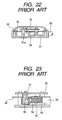
- Fig. 22 is a cross-sectional view showing schematically an overall configuration of a conventional antenna device
- Fig. 23 is an expanded cross-sectional view showing essential parts of the conventional antenna device.
- a configuration of the conventional antenna device will be described with reference to Figs. 22 and 23.
- a ground conductor plate 52 is mounted on a top surface of a boxlike case 51.
- an antenna element 53 is mounted to an upper end portion of a post 51a which is provided to project into the case 51.
- a shield cover 54 is mounted, and a coaxial cable 55 is inserted in a cavity of the shield cover 54.
- An outer conductor 56 of the coaxial cable 55 is soldered to the shield cover 54, and simultaneously a central conductor 57 of the coaxial cable 55 is bent upward and then supported by a holding member 58.
- the central conductor 57 supported by the holding member 58 is connected to the antenna element 53.
- a cuplike cover 59 is mounted on the case 51 to cover the antenna element 53, so that the conventional antenna device is constructed (for example, see Japanese Unexamined Patent Application Publication No. 2003-60414).
- an object of the present invention to provide an inexpensive antenna device has decreased number of components and favorable assembling quality.
- an antenna device comprising an antenna main body portion having a circuit board on which a ground conductor plate made of a metal plate, a radiating conductor plate made of a metal plate and an electronic component are installed to form a desired electrical circuit, and a cable connected to the electrical circuit, in which the ground conductor plate has a stopper portion which is formed by cutting the ground conductor plate and raising the cut portion toward the radiating conductor plate, the stopper portion having an insertion portion provided therebelow, and the cable is inserted into the insertion portion and supported by the stopper portion.
- the cable is a coaxial cable having a central conductor and an outer conductor covering an outside of the central conductor, and the outer conductor is soldered to the stopper portion.
- a cut-out portion is provided in the stopper portion, and the outer conductor is soldered to the stopper portion at a position in the cut-out portion.
- At least a portion of a top surface of the stopper portion is arranged to face the radiating conductor plate in its vicinity of a circumferential edge portion of the radiating conductor plate.
- the stopper portion is arranged along a circumferential edge of the radiating conductor plate.
- the antenna device of the present invention comprises the antenna main body portion having the circuit board on which the ground conductor plate made of the metal plate, the radiating conductor plate made of the metal plate, and the electronic component are mounted to form the desired electrical circuit, and the cable connected to the electrical circuit.
- the ground conductor plate has the stopper portion which is formed by cutting the ground conductor plate and raising the cut portion toward the radiating conductor plate, the stopper portion having an insertion portion provided therebelow, and the cable is inserted into the insertion portion and supported by the stopper portion. According to this configuration, the cable can be supported by the stopper portion which is incorporated into the ground conductor plate. Therefore, an additional component for supporting the cable is not needed, and thus an inexpensive antenna device having decreased number of components and the favorable assembling quality can be obtained.
- the cable is the coaxial cable having the central conductor and the outer conductor covering the outside of the central conductor, and the outer conductor is soldered to the stopper portion.
- the cable can be securely supported.
- a cut-out portion is provided in the stopper portion, and the outer conductor is soldered to the stopper portion at a position in the cut-out portion.
- At least a portion of a top surface of the stopper portion is arranged to face the radiating conductor plate in the vicinity of a circumferential edge portion of the radiating conductor plate.
- the stopper portion is arranged along the outer circumferential edge of the radiating conductor plate.
- the stopper portion is arranged along the outer circumferential edge of the radiating conductor plate.
- Fig. 1 is a plan view showing an antenna device according to the present invention
- Fig. 2 is a plan view showing a state in which a cover is removed, in the antenna device according to the present invention
- Fig. 3 is a cross-sectional view taken along a line 3-3 of Fig. 1
- Fig. 4 is a cross-sectional view taken along a line 4-4 of Fig. 1.
- Fig. 5 is an exploded perspective view showing the antenna device according to the present invention.
- Fig. 6 is a plan view showing a ground conductor plate of the antenna device according to the present invention
- Fig. 7 is a perspective view showing the ground conductor plate of the antenna device according to the present invention
- Fig. 8 is a plan view showing a circuit board of the antenna device according to the present invention
- Fig. 9 is a plan view showing a radiating conductor plate of the antenna device according to the present invention
- Fig. 10 is a front view showing the radiating conductor plate of the antenna device according to the present invention
- Fig. 11 is a bottom view showing the radiating conductor plate of the antenna device according to the present invention.
- Fig. 12 is a plan view showing a cover of the antenna device according to the present invention
- Fig. 13 is a left side view showing the cover of the antenna device according to the present invention
- Fig. 14 is a cross-sectional view showing schematically the cover of the antenna device according to the present invention
- Fig. 15 is a bottom view showing the cover of the antenna device according to the present invention.
- Fig. 16 is a diagram illustrating a first step of a mounting method of the radiating conductor plate on the circuit board, in the antenna device according to the present invention
- Fig. 17 is a diagram illustrating a second step of the mounting method of the radiating conductor plate on the circuit board, in the antenna device according to the present invention
- Fig. 18 is a diagram illustrating a third step of the mounting method of the radiating conductor plate on the circuit board, in the antenna device according to the present invention
- Fig. 19 is a perspective view showing a state in which the mounting of the radiating conductor plate on the circuit board is finished, in the antenna device according to the present invention.
- Fig. 20 is a diagram illustrating a mounting method of a cable to the ground conductor plate, in the antenna device according to the present invention
- Fig. 21 is a perspective view showing a state in which the mounting of the cable to the ground conductor plate is finished, in the antenna device according to the present invention.
- a ground conductor plate 1 made of a metal plate, which serves as a ground conductor, has a plurality of hooking portions 1a, each being formed by cutting the ground conductor plate 1 and raising the cut portion upward in an arch shape in four directions, holes 1b arranged adjacent to the respective hooking portions 1a, a plurality of stopper portions 1c, each being positioned between adjacent two hooking portions 1a and being formed by cutting the ground conductor plate 1 and raising the cut portion upward in an arch shape, cut-out portions 1d, each being provided in a vicinity of a top portion of each stopper portion 1c and being made of a through hole, and insertion portions 1e provided below the respective stopper portions 1c, in particular, as shown in Figs. 6 and 7.
- ground conductor plate 1 has a plurality of bent pieces 1f bent upward, and escape portions 1g provided a plurality of positions which include positions adjacent to the respective bent pieces 1f.
- a rectangular circuit board 2 has a dielectric substrate 3 made of an insulating plate, a wiring pattern 4 provided in the dielectric substrate 3, and a plurality of electrodes 5a, 5b, 5c and 5d provided in four corners of the dielectric substrate 3, in particular, as shown in Fig. 8.
- the electrodes 5a, 5b, 5c and 5d are referred to as first, second, third, and fourth electrodes, respectively.
- first and second electrodes 5a and 5b or the third and fourth electrodes 5c and 5d, which face each other in an oblique direction, have the same area. Further, the first and second electrodes 5a and 5b have the areas smaller than those of the third and fourth electrodes 5c and 5d.
- the dielectric substrate 3 has a plurality of penetrating portions 3a respectively provided at positions of the first to fourth electrodes 5a to 5d as through holes, a plurality of first holes 3b provided in vicinities of an outer circumferential edge, and a plurality of second holes 3c provided in a central portion.
- circuit board 2 electronic components 6 including a short-height chip condenser and so on, or a tall dielectric filter 6a and so on are mounted, so that a desired electrical circuit having a matching circuit, a filter circuit, an amplifying circuit and so on is formed.
- the tall components 6 including the dielectric filter 6a are being arranged in the vicinities of the outer circumferential edge of the circuit board 2.
- Such a circuit board 2 is mounted on the ground conductor plate 1 such that a bottom surface of the circuit board 2 contacts the ground conductor plate 1 while the bent pieces 1f are inserted into the first holes 3b, in particular, as shown in Figs. 3 and 5.
- the bent pieces 1f are soldered to the wiring pattern 4, so that the circuit board 2 is supported by the bent pieces 1f.
- the first to fourth electrodes 5a to 5d face the ground conductor plate 1 with the dielectric substrate 3 interposed therebetween, and then condensers are respectively formed.
- a coaxial cable 7 has a central conductor 7a and a mesh-like outer conductor 7b provided by an insulating covered portion to cover an outside of the central conductor 7a.
- a front end portion of the cable 7 is inserted into the insertion portion 1e of the stopper portion 1c to be in a state as shown in Fig. 21.
- the central conductor 7a is soldered to the wiring pattern 4.
- the outer conductor 7b and the stopper portion 1c are soldered, so that the cable 7 is supported by the stopper portion 1c.
- An octagonal radiating conductor plate 8 made of a metal plate has two feeding portions of first and second feeding portions 9a and 9b, which are formed by cutting the radiating conductor plate 8 and bending the cut portion downward at positions which make a right angle, and adjusting means Z, provided on a line S1 passing through the first feeding portion 9a and a center C, and a line S2 passing through the second feeding portion 9b and the center C, for adjusting an electrical length, in particular, as shown in Figs. 9 to 11.
- the adjusting means Z are provided at the positions of the lines S1 and S2 which are the directions of the electric fields. At the same time, the adjusting means are provided at positions between the central portion and the outer circumferential edge, except for the central portion of the radiating conductor plate 8.
- the adjusting means Z are provided at opposite sides to the first and second feeding portions 9a and 9b therefrom beyond the center C. Further, the adjusting means Z are formed by ladder-like portions which holes 10a and crosspiece portions 10b combine and form. Here, by cutting the crosspiece portions 10b, the electrical lengths extend.
- the radiating conductor plate 8 has a pair of opposing sides 11a and 11b, each being positioned on lines S3 and S4 which pass through the center C and are orthogonal to each other, and four leg pieces 12a, 12b, 12c and 12d provided at positions any where on the lines S3 and S4 up to the first and second opposing sides 11a and 11b, except for the central portion.
- the four leg pieces 12a to 12d are respectively provided at positions spaced by the same distance from the center C to be bent downward. Further, the leg pieces 12a to 12d are provided at positions closer to the center than the first and second opposing sides 11a and 11b.
- the electric field intensity of the radiating conductor plate 8 is made strong in the outer circumferential portion on the lines S1 and S2.
- the leg pieces 12a to 12d are provided at positions, spaced apart from the lines S1 and S2, in which the electric field intensity is relatively weak.
- a locking portion 13 having a first locking piece 13a positioned at the lowest portion and a second locking piece 13b spaced by a predetermined gap from the first locking piece is provided.
- first and second locking pieces 13a and 13b are formed with bent portions which are bent in an opposite direction to each other with each leg piece 12a to 12d as a center.
- the radiating conductor plate 8 As regards the mounting of the radiating conductor plate 8 having such a configuration, first, as shown in Fig. 16, the radiating conductor plate 8 is arranged on the circuit board 2, and then, against the resilience of the leg pieces 12a to 12d, the leg pieces 12a to 12d are bent inward respectively.
- the leg pieces 12a to 12d return to the original states.
- the first locking piece 13a is locked to a rear surface of the circuit board 2 and the second locking piece 13b is locked to a front surface of the circuit board 2.
- the radiating conductor plate 8 is temporally retained to the circuit board 2.
- leg pieces 12a to 12d are respectively soldered and connected to the first to fourth electrodes 5a to 5d, and then the first and second feeding portions 9a and 9b are soldered to the wiring pattern 4 which is provided in vicinities of the second holes 3c.
- an antenna main body portion H is formed.
- leg pieces 12a to 12d and the first and second feeding portions 9a and 9b are not connected to the ground conductor plate 1 by means of the release holes 1g.
- the radiating conductor plate 8 mounted on the circuit board 2 in such a manner is arranged parallel to the ground conductor plate 1 and the circuit board 2 and is spaced by a predetermined gap therefrom. Further, the first electrical length of the radiating conductor plate 8 is determined by a length of the radiating conductor plate 8 on the line S1 and a capacitance of the condenser formed by the electrodes 5a and 5b. In addition, the second electrical length of the radiating conductor plate 8 is determined by a length of the radiating conductor plate 8 on the line S2 and a capacitance of the condenser formed by the electrodes 5c and 5d.
- the length of the radiating conductor plate 8 on the line S1 and the length of the radiating conductor plate 8 on the line S2 are the same, but the capacitance formed by the electrodes 5a and 5b is set to be smaller than the capacitance formed by the electrodes 5c and 5d.
- the first electrical length is smaller than the second electrical length, and then the difference between both electrical lengths is caused. As a result, a circularly polarized wave antenna device is obtained.
- the circuit board 2 is positioned within a planar region of the radiating conductor plate 8.
- the radiating conductor plate 8 when the radiating conductor plate 8 is mounted, upper surfaces of the hooking portions 1a, the stopper portions 1c and the tall electronic component 6a are arranged to face the vicinities of the circumferential edge portion of the radiating conductor plate 8. Further, the front end portions of the bent portions 1f are arranged to face the radiating conductor plate 8, and between the hooking portions 1a, the stopper portions 1c, the tall electronic component 6a and the bent portions 1f, and the radiating conductor plate 8, capacitances are generated.
- the remaining portions 1a and the stopper portions 1c are arranged along the outer circumferential edge of the radiating conductor plate 8.
- the hooking portions 1a and the stopper portions 1c can be formed close to the center C of the radiating conductor plate 8. As a result, it is possible to plan the miniaturization of the antenna device.
- the capacitances of the first to fourth electrodes 5a to 5d, or the capacitances between the hooking portions 1a, the stopper portions 1c, the tall electronic component 6a and the bent portions 1f, and the radiating conductor plate 8 it is possible to lower the frequency, and then it is possible to plan the miniaturization of the antenna device.
- the cuplike cover 14 made of a mold of the insulating material has an octagonal upper wall 14a, eight side walls 14b extending downward from eight sidelines of the upper wall 14a, a receiving portion 14c surrounded by the upper wall 14a and the side walls 14b, a concave portion 14d provided in a lower portion of any one of the side walls 14b, hook-like locking portions 14e provided at insides of lower portions of the side walls 14b for every two side walls, and convex portions 14f projected downward from the lower portions of the side walls 14b on which the locking portions 14e are positioned, in particular, as shown in Figs. 12 to 15.
- the cover 14 overall houses the antenna main body portion H having the radiating conductor plate 8 and the circuit board 2. Further, in the state in which the locking portions 14e are fitted to the remaining portions 1a, the cover 14 is pressed downward (the ground conductor plate 1 side), and then the locking portions 14e are locked to the lower portions of the hooking portions 1a in a snap-fit manner. As a result, the cover 14 is mounted on the ground conductor plate 1.
- the convex portions 14f provided the lower portions of the side walls 14b are engaged with the holes 1b adjacent to the hooking portions 1a. Further, in the concave portion 14d, the cable 7 is positioned and pressed.
- a sealing sheet 15 is formed with a label or the like on one side of which an adhesive is provided.
- the sealing sheet 15 is adhered to the rear surface of the ground conductor plate 1, and then the release holes 1g are blocked.
- the antenna device of the present invention is formed.
Applications Claiming Priority (2)
| Application Number | Priority Date | Filing Date | Title |
|---|---|---|---|
| JP2003397287A JP2005159836A (ja) | 2003-11-27 | 2003-11-27 | アンテナ装置 |
| JP2003397287 | 2003-11-27 |
Publications (1)
| Publication Number | Publication Date |
|---|---|
| EP1536515A1 true EP1536515A1 (fr) | 2005-06-01 |
Family
ID=34463832
Family Applications (1)
| Application Number | Title | Priority Date | Filing Date |
|---|---|---|---|
| EP04027521A Withdrawn EP1536515A1 (fr) | 2003-11-27 | 2004-11-19 | Dispositif d'antenne |
Country Status (2)
| Country | Link |
|---|---|
| EP (1) | EP1536515A1 (fr) |
| JP (1) | JP2005159836A (fr) |
Cited By (7)
| Publication number | Priority date | Publication date | Assignee | Title |
|---|---|---|---|---|
| EP1744396A1 (fr) * | 2005-07-13 | 2007-01-17 | Hirschmann Car Communication GmbH | Antenne de toit pour véhicule avec socle en tôle |
| EP1796206A1 (fr) * | 2005-12-08 | 2007-06-13 | Alps Electric Co., Ltd. | Dispositif d'antenne |
| EP2182579A1 (fr) * | 2008-10-31 | 2010-05-05 | Alps Electric Co., Ltd. | Dispositif d'antenne |
| DE102011011494A1 (de) * | 2011-02-17 | 2012-09-06 | Kathrein-Werke Kg | Patchantenne sowie Verfahren zur Frequenzabstimmung einer derartigen Patchantenne |
| CN103563168A (zh) * | 2011-05-17 | 2014-02-05 | 3M创新有限公司 | 用于集中式建筑物内网络的天线组件 |
| CN106329058A (zh) * | 2015-07-01 | 2017-01-11 | 泰科电子日本合同会社 | 天线装置 |
| DE102016106606B3 (de) * | 2016-04-11 | 2017-03-09 | Wilhelm Sihn Jr. Gmbh & Co. Kg | Fahrzeugantenne |
Citations (8)
| Publication number | Priority date | Publication date | Assignee | Title |
|---|---|---|---|---|
| US5294938A (en) * | 1991-03-15 | 1994-03-15 | Matsushita Electric Works, Ltd. | Concealedly mounted top loaded vehicular antenna unit |
| US5402136A (en) * | 1991-10-04 | 1995-03-28 | Naohisa Goto | Combined capacitive loaded monopole and notch array with slits for multiple resonance and impedance matching pins |
| WO1997041619A1 (fr) * | 1996-04-26 | 1997-11-06 | Dorne & Margolin, Inc. | Combinaison d'antennes pour communications cellulaires et communications par systeme gps |
| US5757327A (en) * | 1994-07-29 | 1998-05-26 | Mitsumi Electric Co., Ltd. | Antenna unit for use in navigation system |
| US6222497B1 (en) * | 1998-11-20 | 2001-04-24 | Smarteq Wireless Ab | Antenna device |
| US6342860B1 (en) * | 2001-02-09 | 2002-01-29 | Centurion Wireless Technologies | Micro-internal antenna |
| WO2002084800A2 (fr) * | 2001-04-10 | 2002-10-24 | Hrl Laboratories, Llc | Antenne a fentes de faible hauteur pour communications pour vehicules et procedes de fabrication et de conception d'une telle antenne |
| JP2003060414A (ja) * | 2001-08-20 | 2003-02-28 | Furukawa Electric Co Ltd:The | アンテナユニット |
-
2003
- 2003-11-27 JP JP2003397287A patent/JP2005159836A/ja not_active Withdrawn
-
2004
- 2004-11-19 EP EP04027521A patent/EP1536515A1/fr not_active Withdrawn
Patent Citations (8)
| Publication number | Priority date | Publication date | Assignee | Title |
|---|---|---|---|---|
| US5294938A (en) * | 1991-03-15 | 1994-03-15 | Matsushita Electric Works, Ltd. | Concealedly mounted top loaded vehicular antenna unit |
| US5402136A (en) * | 1991-10-04 | 1995-03-28 | Naohisa Goto | Combined capacitive loaded monopole and notch array with slits for multiple resonance and impedance matching pins |
| US5757327A (en) * | 1994-07-29 | 1998-05-26 | Mitsumi Electric Co., Ltd. | Antenna unit for use in navigation system |
| WO1997041619A1 (fr) * | 1996-04-26 | 1997-11-06 | Dorne & Margolin, Inc. | Combinaison d'antennes pour communications cellulaires et communications par systeme gps |
| US6222497B1 (en) * | 1998-11-20 | 2001-04-24 | Smarteq Wireless Ab | Antenna device |
| US6342860B1 (en) * | 2001-02-09 | 2002-01-29 | Centurion Wireless Technologies | Micro-internal antenna |
| WO2002084800A2 (fr) * | 2001-04-10 | 2002-10-24 | Hrl Laboratories, Llc | Antenne a fentes de faible hauteur pour communications pour vehicules et procedes de fabrication et de conception d'une telle antenne |
| JP2003060414A (ja) * | 2001-08-20 | 2003-02-28 | Furukawa Electric Co Ltd:The | アンテナユニット |
Non-Patent Citations (1)
| Title |
|---|
| PATENT ABSTRACTS OF JAPAN vol. 2003, no. 06 3 June 2003 (2003-06-03) * |
Cited By (11)
| Publication number | Priority date | Publication date | Assignee | Title |
|---|---|---|---|---|
| EP1744396A1 (fr) * | 2005-07-13 | 2007-01-17 | Hirschmann Car Communication GmbH | Antenne de toit pour véhicule avec socle en tôle |
| EP1796206A1 (fr) * | 2005-12-08 | 2007-06-13 | Alps Electric Co., Ltd. | Dispositif d'antenne |
| EP2182579A1 (fr) * | 2008-10-31 | 2010-05-05 | Alps Electric Co., Ltd. | Dispositif d'antenne |
| DE102011011494A1 (de) * | 2011-02-17 | 2012-09-06 | Kathrein-Werke Kg | Patchantenne sowie Verfahren zur Frequenzabstimmung einer derartigen Patchantenne |
| CN103563168A (zh) * | 2011-05-17 | 2014-02-05 | 3M创新有限公司 | 用于集中式建筑物内网络的天线组件 |
| EP2710670A2 (fr) * | 2011-05-17 | 2014-03-26 | 3M Innovative Properties Company | Ensemble antenne pour un réseau convergé et intégré à des bâtiments |
| EP2710670A4 (fr) * | 2011-05-17 | 2014-11-19 | 3M Innovative Properties Co | Ensemble antenne pour un réseau convergé et intégré à des bâtiments |
| US8947319B2 (en) | 2011-05-17 | 2015-02-03 | 3M Innovative Properties Company | Antenna assembly for converged in-building network |
| CN106329058A (zh) * | 2015-07-01 | 2017-01-11 | 泰科电子日本合同会社 | 天线装置 |
| CN106329058B (zh) * | 2015-07-01 | 2019-12-06 | 泰科电子日本合同会社 | 天线装置 |
| DE102016106606B3 (de) * | 2016-04-11 | 2017-03-09 | Wilhelm Sihn Jr. Gmbh & Co. Kg | Fahrzeugantenne |
Also Published As
| Publication number | Publication date |
|---|---|
| JP2005159836A (ja) | 2005-06-16 |
Similar Documents
| Publication | Publication Date | Title |
|---|---|---|
| US7075486B2 (en) | Circularly polarized wave antenna made of sheet metal with high reliability | |
| EP1536511A1 (fr) | Dispositif d'antenne | |
| US6958732B2 (en) | Small-sized and high-gained antenna-integrated module | |
| US11228109B2 (en) | Antenna device | |
| EP1533867A1 (fr) | Antenne à fente à polarisation circulaire capable d'être miniaturisée facilement | |
| JPH0653733A (ja) | 共振器アンテナ | |
| EP1555722B1 (fr) | Antenne à fente à haut gain dans le zénith | |
| EP1536515A1 (fr) | Dispositif d'antenne | |
| EP1536516B1 (fr) | Dispositif d'antenne à polarisation circulaire | |
| US7046203B2 (en) | Antenna device having miniaturized radiating conductor plate | |
| JP4734808B2 (ja) | カードタイプ無線通信端末装置 | |
| US6972720B2 (en) | Antenna device capable of adjusting frequency | |
| EP1536514B1 (fr) | Dispositif d'antenne | |
| US20090161324A1 (en) | Shielding case, wiring board and electronic module | |
| JP2005203879A (ja) | 複合アンテナ | |
| JP4374285B2 (ja) | 高周波機器の枠体の製造方法 | |
| JP4113016B2 (ja) | チューナ装置 | |
| JP2005159838A (ja) | アンテナ装置 | |
| JP2005159840A (ja) | アンテナ装置 | |
| JP2005159841A (ja) | アンテナ装置 | |
| JP2005159839A (ja) | アンテナ装置 | |
| JP2005203919A (ja) | アンテナ装置 | |
| JP2005159945A (ja) | 円偏波型アンテナ装置 | |
| JP2005159842A (ja) | アンテナ装置 |
Legal Events
| Date | Code | Title | Description |
|---|---|---|---|
| PUAI | Public reference made under article 153(3) epc to a published international application that has entered the european phase |
Free format text: ORIGINAL CODE: 0009012 |
|
| AK | Designated contracting states |
Kind code of ref document: A1 Designated state(s): AT BE BG CH CY CZ DE DK EE ES FI FR GB GR HU IE IS IT LI LU MC NL PL PT RO SE SI SK TR |
|
| AX | Request for extension of the european patent |
Extension state: AL HR LT LV MK YU |
|
| 17P | Request for examination filed |
Effective date: 20050614 |
|
| AKX | Designation fees paid |
Designated state(s): DE FR GB |
|
| STAA | Information on the status of an ep patent application or granted ep patent |
Free format text: STATUS: THE APPLICATION IS DEEMED TO BE WITHDRAWN |
|
| 18D | Application deemed to be withdrawn |
Effective date: 20051229 |