BACKGROUND OF THE INVENTION
1. Field of the Invention
-
The present invention relates to a patch antenna
device which can be suitably used for a GPS antenna or
the like.
2. Description of the Related Art
-
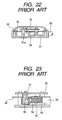
A conventional antenna device will be described with
reference to the accompanying drawings. Fig. 22 is a
cross-sectional view showing schematically an overall
configuration of a conventional antenna device, and Fig.
23 is an expanded cross-sectional view showing essential
parts of the conventional antenna device.
-
Next, a configuration of the conventional antenna
device will be described with reference to Figs. 22 and
23. On a top surface of a boxlike case 51, a ground
conductor plate 52 is mounted. At the same time, to an
upper end portion of a post 51a which is provided to
project into the case 51, an antenna element 53 is
mounted.
-
Further, on a bottom surface of the ground conductor
plate 52, a shield cover 54 is mounted, and a coaxial
cable 55 is inserted in a cavity of the shield cover 54.
An outer conductor 56 of the coaxial cable 55 is soldered
to the shield cover 54, and simultaneously a central
conductor 57 of the coaxial cable 55 is bent upward and
then supported by a holding member 58.
-
And then, the central conductor 57 supported by the
holding member 58 is connected to the antenna element 53.
At the same time, a cuplike cover 59 is mounted on the
case 51 to cover the antenna element 53, so that the
conventional antenna device is constructed (for example,
see Japanese Unexamined Patent Application Publication No.
2003-60414).
-
However, in such a conventional antenna device,
since the outer conductor 56 is soldered to the shield
cover 54, the coaxial cable 55 can be stably mounted. In
this case, however, the shield cover 54, separated from
the ground conductor plate 52, is needed, which results
in increasing the number of components. Consequently,
the manufacturing cost increases, the mounting work
becomes complicated, and the productivity decreases.
SUMMARY OF THE INVENTION
-
Accordingly, it is an object of the present
invention to provide an inexpensive antenna device has
decreased number of components and favorable assembling
quality.
-
In order to solve the above problems, according to a
first aspect of the present invention, there is provided
an antenna device comprising an antenna main body portion
having a circuit board on which a ground conductor plate
made of a metal plate, a radiating conductor plate made
of a metal plate and an electronic component are
installed to form a desired electrical circuit, and a
cable connected to the electrical circuit, in which the
ground conductor plate has a stopper portion which is
formed by cutting the ground conductor plate and raising
the cut portion toward the radiating conductor plate, the
stopper portion having an insertion portion provided
therebelow, and the cable is inserted into the insertion
portion and supported by the stopper portion.
-
Further, according to a second aspect of the present
invention, the cable is a coaxial cable having a central
conductor and an outer conductor covering an outside of
the central conductor, and the outer conductor is
soldered to the stopper portion.
-
Further, according to a third aspect of the present
invention, a cut-out portion is provided in the stopper
portion, and the outer conductor is soldered to the
stopper portion at a position in the cut-out portion.
-
Further, according to a fourth aspect of the present
invention, at least a portion of a top surface of the
stopper portion is arranged to face the radiating
conductor plate in its vicinity of a circumferential edge
portion of the radiating conductor plate.
-
Further, according to a fifth aspect of the present
invention, the stopper portion is arranged along a
circumferential edge of the radiating conductor plate.
-
The antenna device of the present invention
comprises the antenna main body portion having the
circuit board on which the ground conductor plate made of
the metal plate, the radiating conductor plate made of
the metal plate, and the electronic component are mounted
to form the desired electrical circuit, and the cable
connected to the electrical circuit. Further, in the
antenna device of the present invention, the ground
conductor plate has the stopper portion which is formed
by cutting the ground conductor plate and raising the cut
portion toward the radiating conductor plate, the stopper
portion having an insertion portion provided therebelow,
and the cable is inserted into the insertion portion and
supported by the stopper portion. According to this
configuration, the cable can be supported by the stopper
portion which is incorporated into the ground conductor
plate. Therefore, an additional component for supporting
the cable is not needed, and thus an inexpensive antenna
device having decreased number of components and the
favorable assembling quality can be obtained.
-
Further, the cable is the coaxial cable having the
central conductor and the outer conductor covering the
outside of the central conductor, and the outer conductor
is soldered to the stopper portion. Thus, the cable can
be securely supported.
-
Further, a cut-out portion is provided in the
stopper portion, and the outer conductor is soldered to
the stopper portion at a position in the cut-out portion.
Thus, the soldering of the stopper portion and the outer
conductor can be advantageously carried out to securely
support the cable.
-
Further, at least a portion of a top surface of the
stopper portion is arranged to face the radiating
conductor plate in the vicinity of a circumferential edge
portion of the radiating conductor plate. Thus, an
additional capacitance is generated between the stopper
portion and the radiating conductor plate, which makes it
possible to reduce a resonant frequency. Further, it is
also possible to plan the miniaturization of the
radiating conductor plate.
-
Further, the stopper portion is arranged along the
outer circumferential edge of the radiating conductor
plate. Thus, it is possible to arrange a position of the
stopper portion even at a center of the radiating
conductor plate, to miniaturize the device.
BRIEF DESCRIPTION OF THE DRAWINGS
-
- Fig. 1 is a plan view showing an antenna device
according to the present invention;
- Fig. 2 is a plan view showing a state in which a
cover is removed, in the antenna device according to the
present invention;
- Fig. 3 is a cross-sectional view taken along a line
3-3 of Fig. 1;
- Fig. 4 is a cross-sectional view taken along a line
4-4 of Fig. 1;
- Fig. 5 is an exploded perspective view showing the
antenna device according to the present invention;
- Fig. 6 is a plan view showing a ground conductor
plate of the antenna device according to the present
invention;
- Fig. 7 is a perspective view showing the ground
conductor plate of the antenna device according to the
present invention;
- Fig. 8 is a plan view showing a circuit board of the
antenna device according to the present invention;
- Fig. 9 is a plan view showing a radiating conductor
plate of the antenna device according to the present
invention;
- Fig. 10 is a front view showing the radiating
conductor plate of the antenna device according to the
present invention;
- Fig. 11 is a bottom view showing the radiating
conductor plate of the antenna device according to the
present invention;
- Fig. 12 is a plan view showing a cover of the
antenna device according to the present invention;
- Fig. 13 is a left side view showing the cover of the
antenna device according to the present invention;
- Fig. 14 is a cross-sectional view showing
schematically the cover of the antenna device according
to the present invention;
- Fig. 15 is a bottom view showing the cover of the
antenna device according to the present invention;
- Fig. 16 is a diagram illustrating a first step of a
mounting method of the radiating conductor plate on the
circuit board, in the antenna device according to the
present invention;
- Fig. 17 is a diagram illustrating a second step of
the mounting method of the radiating conductor plate on
the circuit board, in the antenna device according to the
present invention;
- Fig. 18 is a diagram illustrating a third step of
the mounting method of the radiating conductor plate on
the circuit board, in the antenna device according to the
present invention;
- Fig. 19 is a perspective view showing a state in
which the mounting of the radiating conductor plate on
the circuit board is finished, in the antenna device
according to the present invention;
- Fig. 20 is a diagram illustrating a mounting method
of a cable to the ground conductor plate, in the antenna
device according to the present invention;
- Fig. 21 is a perspective view showing a state in
which the mounting of the cable to the ground conductor
plate is finished, in the antenna device according to the
present invention;
- Fig. 22 is a cross-sectional view showing
schematically an overall configuration of a conventional
antenna device; and
- Fig. 23 is an expanded cross-sectional view showing
essential parts of the conventional antenna device.
-
DESCRIPTION OF THE PREFERRED EMBODIMENT
-
An antenna device of the present invention will now
be described with reference to the accompanying drawings.
Fig. 1 is a plan view showing an antenna device according
to the present invention, and Fig. 2 is a plan view
showing a state in which a cover is removed, in the
antenna device according to the present invention.
Further, Fig. 3 is a cross-sectional view taken along a
line 3-3 of Fig. 1, and Fig. 4 is a cross-sectional view
taken along a line 4-4 of Fig. 1. In addition, Fig. 5 is
an exploded perspective view showing the antenna device
according to the present invention.
-
Further, Fig. 6 is a plan view showing a ground
conductor plate of the antenna device according to the
present invention, and Fig. 7 is a perspective view
showing the ground conductor plate of the antenna device
according to the present invention. Further, Fig. 8 is a
plan view showing a circuit board of the antenna device
according to the present invention, and Fig. 9 is a plan
view showing a radiating conductor plate of the antenna
device according to the present invention. In addition,
Fig. 10 is a front view showing the radiating conductor
plate of the antenna device according to the present
invention, and Fig. 11 is a bottom view showing the
radiating conductor plate of the antenna device according
to the present invention.
-
Further, Fig. 12 is a plan view showing a cover of
the antenna device according to the present invention,
and Fig. 13 is a left side view showing the cover of the
antenna device according to the present invention. In
addition, Fig. 14 is a cross-sectional view showing
schematically the cover of the antenna device according
to the present invention, and Fig. 15 is a bottom view
showing the cover of the antenna device according to the
present invention.
-
Further, Fig. 16 is a diagram illustrating a first
step of a mounting method of the radiating conductor
plate on the circuit board, in the antenna device
according to the present invention, and Fig. 17 is a
diagram illustrating a second step of the mounting method
of the radiating conductor plate on the circuit board, in
the antenna device according to the present invention.
In addition, Fig. 18 is a diagram illustrating a third
step of the mounting method of the radiating conductor
plate on the circuit board, in the antenna device
according to the present invention, and Fig. 19 is a
perspective view showing a state in which the mounting of
the radiating conductor plate on the circuit board is
finished, in the antenna device according to the present
invention.
-
Further, Fig. 20 is a diagram illustrating a
mounting method of a cable to the ground conductor plate,
in the antenna device according to the present invention,
and Fig. 21 is a perspective view showing a state in
which the mounting of the cable to the ground conductor
plate is finished, in the antenna device according to the
present invention.
-
Next, a configuration of the antenna device of the
present invention will be described with reference to
Figs. 1 to 21. A ground conductor plate 1 made of a
metal plate, which serves as a ground conductor, has a
plurality of hooking portions 1a, each being formed by
cutting the ground conductor plate 1 and raising the cut
portion upward in an arch shape in four directions, holes
1b arranged adjacent to the respective hooking portions
1a, a plurality of stopper portions 1c, each being
positioned between adjacent two hooking portions 1a and
being formed by cutting the ground conductor plate 1 and
raising the cut portion upward in an arch shape, cut-out
portions 1d, each being provided in a vicinity of a top
portion of each stopper portion 1c and being made of a
through hole, and insertion portions 1e provided below
the respective stopper portions 1c, in particular, as
shown in Figs. 6 and 7.
-
Further, the ground conductor plate 1 has a
plurality of bent pieces 1f bent upward, and escape
portions 1g provided a plurality of positions which
include positions adjacent to the respective bent pieces
1f.
-
A rectangular circuit board 2 has a dielectric
substrate 3 made of an insulating plate, a wiring pattern
4 provided in the dielectric substrate 3, and a plurality
of electrodes 5a, 5b, 5c and 5d provided in four corners
of the dielectric substrate 3, in particular, as shown in
Fig. 8. Here, the electrodes 5a, 5b, 5c and 5d are
referred to as first, second, third, and fourth
electrodes, respectively.
-
Further, the first and second electrodes 5a and 5b
or the third and fourth electrodes 5c and 5d, which face
each other in an oblique direction, have the same area.
Further, the first and second electrodes 5a and 5b have
the areas smaller than those of the third and fourth
electrodes 5c and 5d.
-
In addition, the dielectric substrate 3 has a
plurality of penetrating portions 3a respectively
provided at positions of the first to fourth electrodes
5a to 5d as through holes, a plurality of first holes 3b
provided in vicinities of an outer circumferential edge,
and a plurality of second holes 3c provided in a central
portion.
-
And then, on the circuit board 2, electronic
components 6 including a short-height chip condenser and
so on, or a tall dielectric filter 6a and so on are
mounted, so that a desired electrical circuit having a
matching circuit, a filter circuit, an amplifying circuit
and so on is formed.
-
Further, the tall components 6 including the
dielectric filter 6a are being arranged in the vicinities
of the outer circumferential edge of the circuit board 2.
-
Such a circuit board 2 is mounted on the ground
conductor plate 1 such that a bottom surface of the
circuit board 2 contacts the ground conductor plate 1
while the bent pieces 1f are inserted into the first
holes 3b, in particular, as shown in Figs. 3 and 5. In
this situation, the bent pieces 1f are soldered to the
wiring pattern 4, so that the circuit board 2 is
supported by the bent pieces 1f.
-
At this time, the bent pieces 1f pass through the
first holes 3b, and front end portions thereof are
projected upward. At the same time, since release holes
1g of the ground conductor plate 1 are positioned below
the penetrating portions 3a and the second holes 3c of
the circuit board 2, the bottom surface of the circuit
board 2 is being relieved from the ground conductor plate
1.
-
Further, when the circuit board 2 is mounted on the
ground conductor plate 1, the first to fourth electrodes
5a to 5d face the ground conductor plate 1 with the
dielectric substrate 3 interposed therebetween, and then
condensers are respectively formed.
-
A coaxial cable 7 has a central conductor 7a and a
mesh-like outer conductor 7b provided by an insulating
covered portion to cover an outside of the central
conductor 7a. As regards the mounting of the cable 7,
first, as shown in Fig. 20, a front end portion of the
cable 7 is inserted into the insertion portion 1e of the
stopper portion 1c to be in a state as shown in Fig. 21.
-
And then, under the state of Fig. 21, the central
conductor 7a is soldered to the wiring pattern 4. At the
same time, at a position in the cut-out portion 1d, the
outer conductor 7b and the stopper portion 1c are
soldered, so that the cable 7 is supported by the stopper
portion 1c.
-
An octagonal radiating conductor plate 8 made of a
metal plate has two feeding portions of first and second
feeding portions 9a and 9b, which are formed by cutting
the radiating conductor plate 8 and bending the cut
portion downward at positions which make a right angle,
and adjusting means Z, provided on a line S1 passing
through the first feeding portion 9a and a center C, and
a line S2 passing through the second feeding portion 9b
and the center C, for adjusting an electrical length, in
particular, as shown in Figs. 9 to 11.
-
And then, directions of electric fields in the
radiating conductor plate 8 become the directions of the
lines S1 and S2. Further, there exist a first electrical
length which generates in the direction of the line S1
and a second electrical length which generates in the
direction of the line S2.
-
Further, the adjusting means Z are provided at the
positions of the lines S1 and S2 which are the directions
of the electric fields. At the same time, the adjusting
means are provided at positions between the central
portion and the outer circumferential edge, except for
the central portion of the radiating conductor plate 8.
-
In addition, the adjusting means Z are provided at
opposite sides to the first and second feeding portions
9a and 9b therefrom beyond the center C. Further, the
adjusting means Z are formed by ladder-like portions
which holes 10a and crosspiece portions 10b combine and
form. Here, by cutting the crosspiece portions 10b, the
electrical lengths extend.
-
Further, the radiating conductor plate 8 has a pair
of opposing sides 11a and 11b, each being positioned on
lines S3 and S4 which pass through the center C and are
orthogonal to each other, and four leg pieces 12a, 12b,
12c and 12d provided at positions any where on the lines
S3 and S4 up to the first and second opposing sides 11a
and 11b, except for the central portion.
-
The four leg pieces 12a to 12d are respectively
provided at positions spaced by the same distance from
the center C to be bent downward. Further, the leg
pieces 12a to 12d are provided at positions closer to the
center than the first and second opposing sides 11a and
11b.
-
Further, the electric field intensity of the
radiating conductor plate 8 is made strong in the outer
circumferential portion on the lines S1 and S2. However,
the leg pieces 12a to 12d are provided at positions,
spaced apart from the lines S1 and S2, in which the
electric field intensity is relatively weak.
-
Further, in each of end portions of the leg pieces
12a to 12d, a locking portion 13 having a first locking
piece 13a positioned at the lowest portion and a second
locking piece 13b spaced by a predetermined gap from the
first locking piece is provided.
-
And then, the first and second locking pieces 13a
and 13b are formed with bent portions which are bent in
an opposite direction to each other with each leg piece
12a to 12d as a center.
-
As regards the mounting of the radiating conductor
plate 8 having such a configuration, first, as shown in
Fig. 16, the radiating conductor plate 8 is arranged on
the circuit board 2, and then, against the resilience of
the leg pieces 12a to 12d, the leg pieces 12a to 12d are
bent inward respectively.
-
Next, as shown in Fig. 17, convex portions of front
ends of the first and second feeding portions 9a and 9b
are engaged with the second holes 3c, and simultaneously
the locking portions 13 of the leg pieces 12a to 12d are
inserted into the insertion portions 3a respectively.
-
Next, as shown in Fig. 18, if the inwardly bending
forces of the leg pieces 12a to 12d are released, by
means of the resilience of the leg pieces 12a to 12d
themselves, the leg pieces 12a to 12d return to the
original states. At this time, the first locking piece
13a is locked to a rear surface of the circuit board 2
and the second locking piece 13b is locked to a front
surface of the circuit board 2. As a result, as shown in
Fig. 19, the radiating conductor plate 8 is temporally
retained to the circuit board 2.
-
And then, the leg pieces 12a to 12d are respectively
soldered and connected to the first to fourth electrodes
5a to 5d, and then the first and second feeding portions
9a and 9b are soldered to the wiring pattern 4 which is
provided in vicinities of the second holes 3c. With the
circuit board 2 and the radiating conductor plate 8, an
antenna main body portion H is formed.
-
At this time, the leg pieces 12a to 12d and the
first and second feeding portions 9a and 9b are not
connected to the ground conductor plate 1 by means of the
release holes 1g.
-
The radiating conductor plate 8 mounted on the
circuit board 2 in such a manner is arranged parallel to
the ground conductor plate 1 and the circuit board 2 and
is spaced by a predetermined gap therefrom. Further, the
first electrical length of the radiating conductor plate
8 is determined by a length of the radiating conductor
plate 8 on the line S1 and a capacitance of the condenser
formed by the electrodes 5a and 5b. In addition, the
second electrical length of the radiating conductor plate
8 is determined by a length of the radiating conductor
plate 8 on the line S2 and a capacitance of the condenser
formed by the electrodes 5c and 5d.
-
In this example, the length of the radiating
conductor plate 8 on the line S1 and the length of the
radiating conductor plate 8 on the line S2 are the same,
but the capacitance formed by the electrodes 5a and 5b is
set to be smaller than the capacitance formed by the
electrodes 5c and 5d. Thus, the first electrical length
is smaller than the second electrical length, and then
the difference between both electrical lengths is caused.
As a result, a circularly polarized wave antenna device
is obtained.
-
Further, when the radiating conductor plate 8 is
mounted, below the radiating conductor plate 8, the
ground conductor plate 1 having the area larger than that
of the radiating conductor plate 8 exists, and further,
between the radiating conductor plate 8 and the ground
conductor plate 1, the circuit board 2 is positioned
within a planar region of the radiating conductor plate 8.
-
In addition, when the radiating conductor plate 8 is
mounted, upper surfaces of the hooking portions 1a, the
stopper portions 1c and the tall electronic component 6a
are arranged to face the vicinities of the
circumferential edge portion of the radiating conductor
plate 8. Further, the front end portions of the bent
portions 1f are arranged to face the radiating conductor
plate 8, and between the hooking portions 1a, the stopper
portions 1c, the tall electronic component 6a and the
bent portions 1f, and the radiating conductor plate 8,
capacitances are generated.
-
In addition, when the radiating conductor plate 8 is
mounted, the remaining portions 1a and the stopper
portions 1c are arranged along the outer circumferential
edge of the radiating conductor plate 8. Thus, the
hooking portions 1a and the stopper portions 1c can be
formed close to the center C of the radiating conductor
plate 8. As a result, it is possible to plan the
miniaturization of the antenna device.
-
Further, by providing the lengths of the radiating
conductor plate 8 on the lines S1 and S2, the
capacitances of the first to fourth electrodes 5a to 5d,
or the capacitances between the hooking portions 1a, the
stopper portions 1c, the tall electronic component 6a and
the bent portions 1f, and the radiating conductor plate 8,
it is possible to lower the frequency, and then it is
possible to plan the miniaturization of the antenna
device.
-
The cuplike cover 14 made of a mold of the
insulating material has an octagonal upper wall 14a,
eight side walls 14b extending downward from eight
sidelines of the upper wall 14a, a receiving portion 14c
surrounded by the upper wall 14a and the side walls 14b,
a concave portion 14d provided in a lower portion of any
one of the side walls 14b, hook-like locking portions 14e
provided at insides of lower portions of the side walls
14b for every two side walls, and convex portions 14f
projected downward from the lower portions of the side
walls 14b on which the locking portions 14e are
positioned, in particular, as shown in Figs. 12 to 15.
-
The cover 14 overall houses the antenna main body
portion H having the radiating conductor plate 8 and the
circuit board 2. Further, in the state in which the
locking portions 14e are fitted to the remaining portions
1a, the cover 14 is pressed downward (the ground
conductor plate 1 side), and then the locking portions
14e are locked to the lower portions of the hooking
portions 1a in a snap-fit manner. As a result, the cover
14 is mounted on the ground conductor plate 1.
-
At this time, the convex portions 14f provided the
lower portions of the side walls 14b are engaged with the
holes 1b adjacent to the hooking portions 1a. Further,
in the concave portion 14d, the cable 7 is positioned and
pressed.
-
A sealing sheet 15 is formed with a label or the
like on one side of which an adhesive is provided. The
sealing sheet 15 is adhered to the rear surface of the
ground conductor plate 1, and then the release holes 1g
are blocked.
-
With such a configuration, the antenna device of the
present invention is formed.