EP1536480A1 - Semiconductor power device with insulated gate, trenchgate structure and corresponding manufacturing method - Google Patents
Semiconductor power device with insulated gate, trenchgate structure and corresponding manufacturing method Download PDFInfo
- Publication number
- EP1536480A1 EP1536480A1 EP03425764A EP03425764A EP1536480A1 EP 1536480 A1 EP1536480 A1 EP 1536480A1 EP 03425764 A EP03425764 A EP 03425764A EP 03425764 A EP03425764 A EP 03425764A EP 1536480 A1 EP1536480 A1 EP 1536480A1
- Authority
- EP
- European Patent Office
- Prior art keywords
- trench
- gate
- layer
- polysilicon
- formation
- Prior art date
- Legal status (The legal status is an assumption and is not a legal conclusion. Google has not performed a legal analysis and makes no representation as to the accuracy of the status listed.)
- Withdrawn
Links
Images






Classifications
-
- H—ELECTRICITY
- H10—SEMICONDUCTOR DEVICES; ELECTRIC SOLID-STATE DEVICES NOT OTHERWISE PROVIDED FOR
- H10D—INORGANIC ELECTRIC SEMICONDUCTOR DEVICES
- H10D30/00—Field-effect transistors [FET]
- H10D30/60—Insulated-gate field-effect transistors [IGFET]
- H10D30/64—Double-diffused metal-oxide semiconductor [DMOS] FETs
- H10D30/66—Vertical DMOS [VDMOS] FETs
- H10D30/668—Vertical DMOS [VDMOS] FETs having trench gate electrodes, e.g. UMOS transistors
-
- H—ELECTRICITY
- H10—SEMICONDUCTOR DEVICES; ELECTRIC SOLID-STATE DEVICES NOT OTHERWISE PROVIDED FOR
- H10D—INORGANIC ELECTRIC SEMICONDUCTOR DEVICES
- H10D12/00—Bipolar devices controlled by the field effect, e.g. insulated-gate bipolar transistors [IGBT]
- H10D12/01—Manufacture or treatment
- H10D12/031—Manufacture or treatment of IGBTs
- H10D12/032—Manufacture or treatment of IGBTs of vertical IGBTs
- H10D12/038—Manufacture or treatment of IGBTs of vertical IGBTs having a recessed gate, e.g. trench-gate IGBTs
-
- H—ELECTRICITY
- H10—SEMICONDUCTOR DEVICES; ELECTRIC SOLID-STATE DEVICES NOT OTHERWISE PROVIDED FOR
- H10D—INORGANIC ELECTRIC SEMICONDUCTOR DEVICES
- H10D12/00—Bipolar devices controlled by the field effect, e.g. insulated-gate bipolar transistors [IGBT]
- H10D12/411—Insulated-gate bipolar transistors [IGBT]
- H10D12/441—Vertical IGBTs
- H10D12/461—Vertical IGBTs having non-planar surfaces, e.g. having trenches, recesses or pillars in the surfaces of the emitter, base or collector regions
- H10D12/481—Vertical IGBTs having non-planar surfaces, e.g. having trenches, recesses or pillars in the surfaces of the emitter, base or collector regions having gate structures on slanted surfaces, on vertical surfaces, or in grooves, e.g. trench gate IGBTs
-
- H—ELECTRICITY
- H10—SEMICONDUCTOR DEVICES; ELECTRIC SOLID-STATE DEVICES NOT OTHERWISE PROVIDED FOR
- H10D—INORGANIC ELECTRIC SEMICONDUCTOR DEVICES
- H10D62/00—Semiconductor bodies, or regions thereof, of devices having potential barriers
- H10D62/10—Shapes, relative sizes or dispositions of the regions of the semiconductor bodies; Shapes of the semiconductor bodies
- H10D62/13—Semiconductor regions connected to electrodes carrying current to be rectified, amplified or switched, e.g. source or drain regions
- H10D62/149—Source or drain regions of field-effect devices
- H10D62/151—Source or drain regions of field-effect devices of IGFETs
- H10D62/156—Drain regions of DMOS transistors
- H10D62/157—Impurity concentrations or distributions
-
- H—ELECTRICITY
- H10—SEMICONDUCTOR DEVICES; ELECTRIC SOLID-STATE DEVICES NOT OTHERWISE PROVIDED FOR
- H10D—INORGANIC ELECTRIC SEMICONDUCTOR DEVICES
- H10D62/00—Semiconductor bodies, or regions thereof, of devices having potential barriers
- H10D62/10—Shapes, relative sizes or dispositions of the regions of the semiconductor bodies; Shapes of the semiconductor bodies
- H10D62/17—Semiconductor regions connected to electrodes not carrying current to be rectified, amplified or switched, e.g. channel regions
- H10D62/393—Body regions of DMOS transistors or IGBTs
-
- H—ELECTRICITY
- H10—SEMICONDUCTOR DEVICES; ELECTRIC SOLID-STATE DEVICES NOT OTHERWISE PROVIDED FOR
- H10D—INORGANIC ELECTRIC SEMICONDUCTOR DEVICES
- H10D64/00—Electrodes of devices having potential barriers
- H10D64/20—Electrodes characterised by their shapes, relative sizes or dispositions
- H10D64/27—Electrodes not carrying the current to be rectified, amplified, oscillated or switched, e.g. gates
- H10D64/311—Gate electrodes for field-effect devices
- H10D64/411—Gate electrodes for field-effect devices for FETs
- H10D64/511—Gate electrodes for field-effect devices for FETs for IGFETs
- H10D64/512—Disposition of the gate electrodes, e.g. buried gates
- H10D64/513—Disposition of the gate electrodes, e.g. buried gates within recesses in the substrate, e.g. trench gates, groove gates or buried gates
-
- H—ELECTRICITY
- H10—SEMICONDUCTOR DEVICES; ELECTRIC SOLID-STATE DEVICES NOT OTHERWISE PROVIDED FOR
- H10D—INORGANIC ELECTRIC SEMICONDUCTOR DEVICES
- H10D30/00—Field-effect transistors [FET]
- H10D30/60—Insulated-gate field-effect transistors [IGFET]
- H10D30/64—Double-diffused metal-oxide semiconductor [DMOS] FETs
- H10D30/66—Vertical DMOS [VDMOS] FETs
- H10D30/665—Vertical DMOS [VDMOS] FETs having edge termination structures
-
- H—ELECTRICITY
- H10—SEMICONDUCTOR DEVICES; ELECTRIC SOLID-STATE DEVICES NOT OTHERWISE PROVIDED FOR
- H10D—INORGANIC ELECTRIC SEMICONDUCTOR DEVICES
- H10D64/00—Electrodes of devices having potential barriers
- H10D64/01—Manufacture or treatment
- H10D64/013—Manufacture or treatment of electrodes having a conductor capacitively coupled to a semiconductor by an insulator
- H10D64/01302—Manufacture or treatment of electrodes having a conductor capacitively coupled to a semiconductor by an insulator the insulator being formed after the semiconductor body, the semiconductor being silicon
- H10D64/01304—Manufacture or treatment of electrodes having a conductor capacitively coupled to a semiconductor by an insulator the insulator being formed after the semiconductor body, the semiconductor being silicon characterised by the conductor
- H10D64/01326—Aspects related to lithography, isolation or planarisation of the conductor
- H10D64/0133—Aspects related to lithography, isolation or planarisation of the conductor at least part of the entire electrode being a sidewall spacer, being formed by transformation under a mask or being formed by plating at a sidewall
-
- H—ELECTRICITY
- H10—SEMICONDUCTOR DEVICES; ELECTRIC SOLID-STATE DEVICES NOT OTHERWISE PROVIDED FOR
- H10D—INORGANIC ELECTRIC SEMICONDUCTOR DEVICES
- H10D64/00—Electrodes of devices having potential barriers
- H10D64/20—Electrodes characterised by their shapes, relative sizes or dispositions
- H10D64/27—Electrodes not carrying the current to be rectified, amplified, oscillated or switched, e.g. gates
- H10D64/311—Gate electrodes for field-effect devices
- H10D64/411—Gate electrodes for field-effect devices for FETs
- H10D64/511—Gate electrodes for field-effect devices for FETs for IGFETs
- H10D64/517—Gate electrodes for field-effect devices for FETs for IGFETs characterised by the conducting layers
- H10D64/518—Gate electrodes for field-effect devices for FETs for IGFETs characterised by the conducting layers characterised by their lengths or sectional shapes
-
- H—ELECTRICITY
- H10—SEMICONDUCTOR DEVICES; ELECTRIC SOLID-STATE DEVICES NOT OTHERWISE PROVIDED FOR
- H10D—INORGANIC ELECTRIC SEMICONDUCTOR DEVICES
- H10D64/00—Electrodes of devices having potential barriers
- H10D64/60—Electrodes characterised by their materials
- H10D64/66—Electrodes having a conductor capacitively coupled to a semiconductor by an insulator, e.g. MIS electrodes
- H10D64/661—Electrodes having a conductor capacitively coupled to a semiconductor by an insulator, e.g. MIS electrodes the conductor comprising a layer of silicon contacting the insulator, e.g. polysilicon having vertical doping variation
- H10D64/662—Electrodes having a conductor capacitively coupled to a semiconductor by an insulator, e.g. MIS electrodes the conductor comprising a layer of silicon contacting the insulator, e.g. polysilicon having vertical doping variation the conductor further comprising additional layers, e.g. multiple silicon layers having different crystal structures
- H10D64/663—Electrodes having a conductor capacitively coupled to a semiconductor by an insulator, e.g. MIS electrodes the conductor comprising a layer of silicon contacting the insulator, e.g. polysilicon having vertical doping variation the conductor further comprising additional layers, e.g. multiple silicon layers having different crystal structures the additional layers comprising a silicide layer contacting the layer of silicon, e.g. polycide gates
Definitions
- the present invention relates to a semiconductor power device with insulated gate and improved trench-gate structure.
- the invention relates to a device of said type wherein the trench-gate structure is realised on a semiconductor substrate covered by at least an epitaxial layer and through a trench realised in the semiconductor and filled in with a polysilicon layer to form the device gate region; a dielectric coating being provided on the trench inner and bottom walls.
- the invention also relates to a manufacturing method of said semiconductor power device.
- the invention particularly relates, but not exclusively, to a realisation of the trench-gate structure of a power device with a simplified process and improved performances and the following description is made with reference to this field of application for convenience of illustration only.
- the performances thereof derive from the fact of having combined the advantages of a bipolar transistor (high conductivity) and those of a field-effect MOS transistor (control voltage with high input resistance), the second transistor driving the first base current.
- IGBT devices can be generally manufactured in two versions: a first one called “planar gate” and another one called “trench-gate”, whose cross-section can be seen in figure 1.
- the structure of a "trench-gate" IGBT device comprises a substrate 1 of p+ semiconductor material whereon an epitaxial layer is grown, split into buffer layer 2 and drift layer 3, of the n+ and n- type respectively. Two differently-doped p regions are formed on the layer 3: the body 4 and a deep body 5. The source region 6 of the n type is integrated in the body region.
- the trench-gate structure is realised by means of a trench realised in the silicon filled in with a polysilicon layer to form the gate region 7 and separated from the other portions by means of a silicon oxide coating 8 grown on the trench walls.
- a deposit of dielectric 9 and a metal contact 10 complete the device.
- Regions 1 and 3 are the conduction electrodes of the bipolar transistor, while the MOS transistor comprises the source 6 and drift layer 3 regions and the gate 7.
- the technical problem underlying the present invention is to provide a manufacturing method of a semiconductor power device with insulated gate and improved trench-gate structure, the method having such features as to allow the drawbacks mentioned with reference to the prior art to be overcome.
- the solution idea underlying the present invention is to realise the trench-gate structure by inserting a conductive spacer, for example of polysilicon, on the trench-gate inner walls.
- a power device 20 with insulated gate and improved trench-gate structure realised according to the invention by means of a conductive spacer, for example of polysilicon, is described.
- the method thus provides the following steps:
- the coating layer 28 is an oxide layer, while the conductive layer 27' is a polysilicon layer.
- the etching to realise the polysilicon spacer 30 can be performed without mask.
- the device gate structure will be formed by polysilicon stripes, two independent stripes 24, 25 for each trench, contacted by the metal gate 26 after etching the intermediate passivation 31 at the contact opening.
- the spacer 30 comprises the two independent conductive stripes 24, 25 being essentially parallel to each other, which are close to the coating layer 28 and realised only in correspondence with the trench 29 inner walls. On the contrary, the spacer 30 is not realised on the trench 29 bottom.
- the spacer 30 etching can be performed with the mask in order not to etch the polysilicon in the edge region to realise the gate contact and the field-plate 33 in this region 26, as shown in figure 8.
- the portion of the device active area covered by the gate oxide only concerns the channel region; in fact the polysilicon is recessed from the trench top and it is removed from the trench bottom; this involves a decrease in the stray capacity linked to the device gate terminal (considerable improvement with respect to the structure shown in figure 1).
- the polysilicon layer must not completely close the trench to allow the trench lower portion to be subsequently etched.
- the thermal budget attributed to the dopant realising the device source is such that the source/body junction is deeper than the level whereto the polysilicon layer is recessed.
- the final device structure shown in figure 6 can be further improved by means of some tricks being described hereafter.
- the device and method according to the invention solve the technical problem and they allow a semiconductor power device with insulated gate and trench-gate to be obtained, equipped with a conductive spacer, for example of polysilicon, and with definitely better production yields and performance features than prior art solutions.
Landscapes
- Electrodes Of Semiconductors (AREA)
Abstract
Description
- Figure 1 is a cross-sectional schematic view of an IGBT or Power MOS power device with insulated trench-gate realised according to the prior art; the bird-beak structure of the silicon oxide being also underlined in the oval;
- Figure 2 is a blowup of the circled area of the previous figure 1;
- Figure 3 schematically shows a possible known solution with sloping trench walls to avoid the bird-beak;
- Figure 4 schematically shows a further known solution providing a gate oxide region adding stray capacity outside the channel region;
- Figure 5 schematically shows an improved structure with respect to figure 4 with recessed polysilicon and with the trench bottom being filled in with thick oxide;
- Figure 6 is a schematic view of a device with the improved trench-gate realised according to the invention;
- Figure 7 is a three-dimensional schematic view of the device of figure 6 with the trench-gate realised according to the invention;
- Figure 8 is a three-dimensional schematic view of the device realised according to the invention with a different polysilicon structure etching;
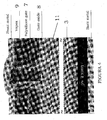
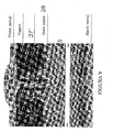
- Figure 9 is a cross-sectional schematic view of the device according to the invention with a drain engineering implant for a low-voltage MOS power;
- Figure 10 is a schematic view of the device according to the invention with an additional enrichment for an IGBT;
- Figure 11 is a cross-sectional schematic view of the device realised according to the invention with an additional silicide layer on the spacer;
- Figure 12 is a cross-sectional schematic view of the device according to the invention with an additional micro trench to realise a body-source short;
- Figure 13 shows the almost final structure of the device according to the invention wherein the contact opening is performed through the etch-back of an intermediate passivation layer.
- a starting
substrate 1 of the N+ type for a MOS power or of the P+ type for an IGBT; - epitaxial growth of the N- type (drift layer) 3 with possible preventive
growth of a buffer layer of the
N+ type 2 at the interface with the substrate; - realisation of edge structures of the
power device 20 by means of a field oxide and/or afield ring 15 of the P type implanted in the device peripheral region, as it can be better seen in figure 8. This implant is also used for realising the device mesh; - exposure of the device active area by removing the thick oxide;
- realisation of the
body structure 4 by means of an opencast implant of the P type; - realisation of the device deep body structure 5 by means of an implant of the P+ type with photoresist mask;
- realisation of the
source structure 6 by means of an implant of the N+ type with photoresist mask; - alignment of a hard mask for etching the semiconductor and
forming a
trench 29 to realise the gate region; - dry anisotropic etching of the semiconductor to realise a
trench 29 having a U-profile in the lower or bottom portion; - hard mask removal;
- cleaning and sacrificial oxidation of the inner walls of the
trench 29 with subsequent oxide removal; - formation of a
coating layer 28 coating thetrench 29, to realise a dielectric gate layer, for example through oxidation; - deposit of a conductive layer 27', for example of polysilicon, for the
partial filling of the
trench 29; it is important that the trench is not completely closed, as it will be apparent from the following description; - formation of a
conductive spacer 30 through dry anisotropic etching of the previously deposited layer 27' to define agate 27 of thedevice 20. The etching has the end-point on thegate coating layer 28 both on the device top and in thetrench 29 bottom; - filling of the
trench 29 by means of theintermediate passivation dielectric 31; - continuation of the manufacturing process to define
front metallisation contacts 32, final passivation and back metallisation according to the prior art.
- In the case of a low-voltage MOS power, realisation of a "drain
engineering" implant 23 after forming the trench. This implant would
serve to impoverish the
drift layer 3 region under the trench to impose, in the same region, a lower electric field slope. It is worth underlying that this trick would generate a self-aligned structure. The resulting structure is shown in figure 9. - In the case of an IGBT, realisation of an
enrichment implant 18, as shown in figure 10, after forming the trench in thedrift layer 3 region under thetrench 29. This enrichment would favour, in this region, the effect, substantiated in literature, of the PIN diode formed by the P+ regions of thesubstrate 1, N- regions of thedrift layer 3 and Nenrichment regions 18 under the trench. In this case too, the structure is self-aligned. - Formation of a
silicide layer 19, as shown in figure 11, on thepolysilicon spacer 30 defining thegate 27 of thedevice 20, to decrease the distributed gate resistance. Thislayer 19 is realised by sputtering a thin metal layer, sintering the silicide through a thermal process and removing the unsintered metal by acqua regia wet etching. In this case too, the process is self-aligned, i.e. it does not require additional phtotechniques. In fact, the silicide layer is formed only on the polysilicon, since the remaining silicon is covered by the gate oxide, even in the trench bottom. - In view of the number reduction of the masks being used, the dopant
constituting the source can be implanted opencast and a body-
source 34 short can be realised by means of a micro-trench 35 realised in the silicon in the contact opening step. The resulting structure is shown in figure 12 showing the portion comprised between two trench-gates 27 by means of themicrotrench 35. - The contact opening can be performed through the etchback of the
intermediate passivation dielectric 31. It thus results that theintermediate passivation dielectric 31 is completely comprised in the trench in thedevice 20 active area, as shown in figure 13. In this solution it is necessary to keep a convenient edge between the polysilicon recess level and the intermediate passivation dielectric etchback.
Claims (21)
- A semiconductor power device (20) with insulated gate and improved trench-gate structure, of the type wherein the trench-gate structure is realised on a semiconductor substrate (1) covered by at least an epitaxial layer (3) and by means of a trench (29) realised in the semiconductor to form the device gate region (27); a dielectric coating (28) being provided on the inner and bottom walls of the trench (29), characterised in that said gate region (27) comprises a conductive spacer layer (30) on said coating layer (28) only in correspondence with the inner walls of the trench (29).
- A device according to claim 1, characterised in that said spacer layer (30) is made of polysilicon.
- A device according to claim 1, characterised in that the epitaxial layer (3) under the trench (29) is interested by a drain implant (23).
- A device according to claim 1, characterised in that the epitaxial layer (3) under the trench 29) is interested by an enrichment implant (18).
- A device according to claim 2, characterised in that it comprises a silicide layer (19) on the polysilicon spacer (30) defining the gate (27) of the device (20), to decrease the distributed gate resistance.
- A device according to claim 2, characterised in that the trench (29) bottom is free from polysilicon.
- A device according to claim 1, characterised in that said trench (29) is filled in with intermediate passivation dielectric (31).
- A device according to claim 1, characterised in that said device is provided with a body region and a source region being short-circuited with each other by means of a microtrench.
- A device according to claim 1, characterised in that said intermediate passivation dielectric (31) is completely comprised in said trench (29).
- A manufacturing method of a power device with insulated gate and improved trench-gate structure, of the type providing at least a step of:semiconductor etching and formation of a trench (29) to realise said trench-gate structure;formation of a gate coating layer (28) of the inner and bottom walls of said trench (29), characterised in that it further comprises:a deposit of a conductive layer (27') for the partial filling of the trench (29);the formation of a polysilicon spacer (30) through anisotropic dry etching of the conductive layer (27').
- A method according to claim 10, characterised in that said conductive layer (27') is made of polysilicon.
- A method according to claim 10, characterised in that said semiconductor etching is of the anisotropic dry type to realise a trench (29) with U-profile in the bottom portion or wall.
- A method according to claim 10, characterised in that, after forming the trench (29), it provides a cleaning and sacrificial oxidation of the inner walls of the trench (29) with subsequent oxide removal.
- A method according to claim 11, characterised in that said anisotropic dry etching step of the polysilicon layer (28) has an end-point on the gate coating layer (28) both on the device upper portion and on the trench (29) bottom.
- A method according to claim 10, characterised in that, after realising the spacer (30), it provides the filling of the trench (29) by means of an intermediate passivation dielectric (31).
- A method according to claim 10, characterised in that it provides the realisation of a "drain engineering" implant (23) after forming the trench (29) to impoverish said epitaxial layer (3) under the trench (29) to impose a lower electric field slope.
- A method according to claim 10, characterised in that it provides the realisation of an enrichment implant (18) after forming the trench (29) and in the epitaxial layer (3) region under the trench (29).
- A method according to claim 11, characterised in that it provides the formation of a silicide layer (19) on the polysilicon spacer (30) defining the gate (27) of the device (20) to decrease the distributed gate resistance.
- A method according to claim 18, characterised in that said silicide layer (19) is realised by sputtering a thin metal layer, with following silicide sintering by means of a thermal process and removal of the unsintered metal by wet etching.
- A method according to claim 15, characterised in that it provides a contact opening step through the etchback of the intermediate passivation dielectric (31).
- A method according to claim 15, characterised in that it provides the further steps of:formation of body and source regions in the substrate,formation of a micro-trench in the substrate to realise a short-circuit between said body and source regions.
Priority Applications (2)
| Application Number | Priority Date | Filing Date | Title |
|---|---|---|---|
| EP03425764A EP1536480A1 (en) | 2003-11-28 | 2003-11-28 | Semiconductor power device with insulated gate, trenchgate structure and corresponding manufacturing method |
| US10/993,917 US7205607B2 (en) | 2003-11-28 | 2004-11-19 | Semiconductor power device with insulated gate and trench-gate structure and corresponding manufacturing method |
Applications Claiming Priority (1)
| Application Number | Priority Date | Filing Date | Title |
|---|---|---|---|
| EP03425764A EP1536480A1 (en) | 2003-11-28 | 2003-11-28 | Semiconductor power device with insulated gate, trenchgate structure and corresponding manufacturing method |
Publications (1)
| Publication Number | Publication Date |
|---|---|
| EP1536480A1 true EP1536480A1 (en) | 2005-06-01 |
Family
ID=34443161
Family Applications (1)
| Application Number | Title | Priority Date | Filing Date |
|---|---|---|---|
| EP03425764A Withdrawn EP1536480A1 (en) | 2003-11-28 | 2003-11-28 | Semiconductor power device with insulated gate, trenchgate structure and corresponding manufacturing method |
Country Status (2)
| Country | Link |
|---|---|
| US (1) | US7205607B2 (en) |
| EP (1) | EP1536480A1 (en) |
Cited By (5)
| Publication number | Priority date | Publication date | Assignee | Title |
|---|---|---|---|---|
| US7205607B2 (en) | 2003-11-28 | 2007-04-17 | Stmicroelectronics S.R.L | Semiconductor power device with insulated gate and trench-gate structure and corresponding manufacturing method |
| EP2388805A1 (en) * | 2010-05-20 | 2011-11-23 | International Rectifier Corporation | Method for fabricating a shallow and narrow trench fet and related structures |
| US8637369B2 (en) | 2008-12-31 | 2014-01-28 | Stmicroelectronics S.R.L. | Method for manufacturing an integrated power device having gate structures within trenches |
| CN110034182A (en) * | 2019-03-13 | 2019-07-19 | 上海华虹宏力半导体制造有限公司 | The manufacturing method of trench-gate device with shield grid |
| CN111128725A (en) * | 2018-10-30 | 2020-05-08 | 株洲中车时代电气股份有限公司 | A kind of IGBT device preparation method |
Families Citing this family (14)
| Publication number | Priority date | Publication date | Assignee | Title |
|---|---|---|---|---|
| US20070249133A1 (en) * | 2006-04-11 | 2007-10-25 | International Business Machines Corporation | Conductive spacers for semiconductor devices and methods of forming |
| US8093621B2 (en) * | 2008-12-23 | 2012-01-10 | Power Integrations, Inc. | VTS insulated gate bipolar transistor |
| US7858506B2 (en) | 2008-06-18 | 2010-12-28 | Micron Technology, Inc. | Diodes, and methods of forming diodes |
| US7964912B2 (en) | 2008-09-18 | 2011-06-21 | Power Integrations, Inc. | High-voltage vertical transistor with a varied width silicon pillar |
| US20100155831A1 (en) * | 2008-12-20 | 2010-06-24 | Power Integrations, Inc. | Deep trench insulated gate bipolar transistor |
| US7871882B2 (en) | 2008-12-20 | 2011-01-18 | Power Integrations, Inc. | Method of fabricating a deep trench insulated gate bipolar transistor |
| IT1396561B1 (en) | 2009-03-13 | 2012-12-14 | St Microelectronics Srl | METHOD FOR REALIZING A POWER DEVICE WITH A TRENCH-GATE STRUCTURE AND ITS DEVICE |
| CN101847603B (en) * | 2009-03-26 | 2013-06-05 | 尼克森微电子股份有限公司 | Manufacturing method and structure of trench power semiconductor with low gate charge |
| WO2011116524A1 (en) * | 2010-03-25 | 2011-09-29 | 香港商莫斯飞特半导体有限公司 | Trench type semiconductor device having low gate resistance and manufacturing method thereof |
| US8653600B2 (en) | 2012-06-01 | 2014-02-18 | Power Integrations, Inc. | High-voltage monolithic schottky device structure |
| US10325988B2 (en) | 2013-12-13 | 2019-06-18 | Power Integrations, Inc. | Vertical transistor device structure with cylindrically-shaped field plates |
| US9543396B2 (en) | 2013-12-13 | 2017-01-10 | Power Integrations, Inc. | Vertical transistor device structure with cylindrically-shaped regions |
| DE102014114230B4 (en) | 2014-09-30 | 2021-10-07 | Infineon Technologies Ag | Semiconductor device and manufacturing method therefor |
| JP6584857B2 (en) * | 2015-08-11 | 2019-10-02 | 株式会社東芝 | Semiconductor device |
Citations (8)
| Publication number | Priority date | Publication date | Assignee | Title |
|---|---|---|---|---|
| US4767722A (en) * | 1986-03-24 | 1988-08-30 | Siliconix Incorporated | Method for making planar vertical channel DMOS structures |
| US4893160A (en) * | 1987-11-13 | 1990-01-09 | Siliconix Incorporated | Method for increasing the performance of trenched devices and the resulting structure |
| US5168331A (en) * | 1991-01-31 | 1992-12-01 | Siliconix Incorporated | Power metal-oxide-semiconductor field effect transistor |
| US5401677A (en) * | 1993-12-23 | 1995-03-28 | International Business Machines Corporation | Method of metal silicide formation in integrated circuit devices |
| US20010006836A1 (en) * | 1994-02-04 | 2001-07-05 | Katsumi Nakamura | Method of forming a trench mos gate on a power semiconductor device |
| EP1244150A2 (en) * | 2001-03-19 | 2002-09-25 | Kabushiki Kaisha Toshiba | Vertical MOSFET having a trench gate electrode and method of making the same |
| US20020158287A1 (en) | 2001-03-21 | 2002-10-31 | Naoto Fujishima | Trench-type MOSFET having a reduced device pitch and on-resistance |
| WO2003010827A2 (en) * | 2001-07-24 | 2003-02-06 | Koninklijke Philips Electronics N.V. | Trench-gate semiconductor devices, and their manufacture |
Family Cites Families (5)
| Publication number | Priority date | Publication date | Assignee | Title |
|---|---|---|---|---|
| US5214305A (en) * | 1990-08-28 | 1993-05-25 | United Microelectronics Corporation | Polycide gate MOSFET for integrated circuits |
| US6580123B2 (en) * | 2000-04-04 | 2003-06-17 | International Rectifier Corporation | Low voltage power MOSFET device and process for its manufacture |
| US6573560B2 (en) * | 2001-11-06 | 2003-06-03 | Fairchild Semiconductor Corporation | Trench MOSFET with reduced Miller capacitance |
| EP1536480A1 (en) | 2003-11-28 | 2005-06-01 | STMicroelectronics S.r.l. | Semiconductor power device with insulated gate, trenchgate structure and corresponding manufacturing method |
| JP3930486B2 (en) * | 2004-02-26 | 2007-06-13 | 株式会社東芝 | Semiconductor device and manufacturing method thereof |
-
2003
- 2003-11-28 EP EP03425764A patent/EP1536480A1/en not_active Withdrawn
-
2004
- 2004-11-19 US US10/993,917 patent/US7205607B2/en not_active Expired - Lifetime
Patent Citations (8)
| Publication number | Priority date | Publication date | Assignee | Title |
|---|---|---|---|---|
| US4767722A (en) * | 1986-03-24 | 1988-08-30 | Siliconix Incorporated | Method for making planar vertical channel DMOS structures |
| US4893160A (en) * | 1987-11-13 | 1990-01-09 | Siliconix Incorporated | Method for increasing the performance of trenched devices and the resulting structure |
| US5168331A (en) * | 1991-01-31 | 1992-12-01 | Siliconix Incorporated | Power metal-oxide-semiconductor field effect transistor |
| US5401677A (en) * | 1993-12-23 | 1995-03-28 | International Business Machines Corporation | Method of metal silicide formation in integrated circuit devices |
| US20010006836A1 (en) * | 1994-02-04 | 2001-07-05 | Katsumi Nakamura | Method of forming a trench mos gate on a power semiconductor device |
| EP1244150A2 (en) * | 2001-03-19 | 2002-09-25 | Kabushiki Kaisha Toshiba | Vertical MOSFET having a trench gate electrode and method of making the same |
| US20020158287A1 (en) | 2001-03-21 | 2002-10-31 | Naoto Fujishima | Trench-type MOSFET having a reduced device pitch and on-resistance |
| WO2003010827A2 (en) * | 2001-07-24 | 2003-02-06 | Koninklijke Philips Electronics N.V. | Trench-gate semiconductor devices, and their manufacture |
Cited By (9)
| Publication number | Priority date | Publication date | Assignee | Title |
|---|---|---|---|---|
| US7205607B2 (en) | 2003-11-28 | 2007-04-17 | Stmicroelectronics S.R.L | Semiconductor power device with insulated gate and trench-gate structure and corresponding manufacturing method |
| US8637369B2 (en) | 2008-12-31 | 2014-01-28 | Stmicroelectronics S.R.L. | Method for manufacturing an integrated power device having gate structures within trenches |
| US8664713B2 (en) | 2008-12-31 | 2014-03-04 | Stmicroelectronics S.R.L. | Integrated power device on a semiconductor substrate having an improved trench gate structure |
| US9520468B2 (en) | 2008-12-31 | 2016-12-13 | Stmicroelectronics S.R.L. | Integrated power device on a semiconductor substrate having an improved trench gate structure |
| EP2388805A1 (en) * | 2010-05-20 | 2011-11-23 | International Rectifier Corporation | Method for fabricating a shallow and narrow trench fet and related structures |
| US9653597B2 (en) | 2010-05-20 | 2017-05-16 | Infineon Technologies Americas Corp. | Method for fabricating a shallow and narrow trench FET and related structures |
| CN111128725A (en) * | 2018-10-30 | 2020-05-08 | 株洲中车时代电气股份有限公司 | A kind of IGBT device preparation method |
| CN111128725B (en) * | 2018-10-30 | 2023-05-30 | 株洲中车时代半导体有限公司 | A kind of IGBT device preparation method |
| CN110034182A (en) * | 2019-03-13 | 2019-07-19 | 上海华虹宏力半导体制造有限公司 | The manufacturing method of trench-gate device with shield grid |
Also Published As
| Publication number | Publication date |
|---|---|
| US7205607B2 (en) | 2007-04-17 |
| US20050145977A1 (en) | 2005-07-07 |
Similar Documents
| Publication | Publication Date | Title |
|---|---|---|
| JP5500898B2 (en) | Method of manufacturing a metal-insulator-semiconductor device having a trench gate electrode | |
| CN102034712B (en) | Method and device for forming shielded gate trench field effect transistor with three masks | |
| US8394702B2 (en) | Method for making dual gate oxide trench MOSFET with channel stop using three or four masks process | |
| JP4834228B2 (en) | Method of manufacturing a trench semiconductor device with a gate oxide layer having a plurality of thicknesses | |
| US7361555B2 (en) | Trench-gate transistors and their manufacture | |
| US7205607B2 (en) | Semiconductor power device with insulated gate and trench-gate structure and corresponding manufacturing method | |
| US6921699B2 (en) | Method for manufacturing a semiconductor device with a trench termination | |
| US20090085107A1 (en) | Trench MOSFET with thick bottom oxide tub | |
| KR20040033313A (en) | Edge termination in a trench-gate mosfet | |
| JP2005524970A (en) | Trench type power MOS gate device | |
| CN108428743B (en) | Metal/polysilicon gate trench power MOSFET and method of forming the same | |
| TW202240907A (en) | A split-gate trench mosfet | |
| TWI803288B (en) | Integrated planar-trench gate power mosfet | |
| US7906388B2 (en) | Semiconductor device and method for manufacture | |
| US12272739B2 (en) | Fin-based laterally-diffused metal-oxide semiconductor field effect transistor | |
| CN113964038B (en) | Fabrication method of trench gate MOSFET device | |
| JP3965027B2 (en) | Method for manufacturing trench gate type MIS device having thick polysilicon insulating layer at bottom of trench | |
| US20070063272A1 (en) | Semiconductor power device with insulated gate formed in a trench, and manufacturing process thereof | |
| US6800917B2 (en) | Bladed silicon-on-insulator semiconductor devices and method of making | |
| EP1536463A1 (en) | Method for manufacturing a power device with insulated trench-gate having controlled channel length and corresponding device | |
| US20040222485A1 (en) | Bladed silicon-on-insulator semiconductor devices and method of making | |
| TW456049B (en) | Trench-type metal oxide semiconductor stop structure | |
| CN101506956A (en) | Manufacturing method of semiconductor device | |
| TWI808856B (en) | Bottom source trench mosfet with shield electrode | |
| JPH04368182A (en) | Semiconductor device and manufacture thereof |
Legal Events
| Date | Code | Title | Description |
|---|---|---|---|
| PUAI | Public reference made under article 153(3) epc to a published international application that has entered the european phase |
Free format text: ORIGINAL CODE: 0009012 |
|
| AK | Designated contracting states |
Kind code of ref document: A1 Designated state(s): AT BE BG CH CY CZ DE DK EE ES FI FR GB GR HU IE IT LI LU MC NL PT RO SE SI SK TR |
|
| AX | Request for extension of the european patent |
Extension state: AL LT LV MK |
|
| 17P | Request for examination filed |
Effective date: 20051125 |
|
| AKX | Designation fees paid |
Designated state(s): DE FR GB IT |
|
| 17Q | First examination report despatched |
Effective date: 20060717 |
|
| RAP1 | Party data changed (applicant data changed or rights of an application transferred) |
Owner name: STMICROELECTRONICS SRL |
|
| RAP1 | Party data changed (applicant data changed or rights of an application transferred) |
Owner name: STMICROELECTRONICS SRL |
|
| STAA | Information on the status of an ep patent application or granted ep patent |
Free format text: STATUS: THE APPLICATION HAS BEEN WITHDRAWN |
|
| 18W | Application withdrawn |
Effective date: 20120822 |