EP1536343B1 - Universal controller for peripheral devices in a computing system - Google Patents
Universal controller for peripheral devices in a computing system Download PDFInfo
- Publication number
- EP1536343B1 EP1536343B1 EP20040257126 EP04257126A EP1536343B1 EP 1536343 B1 EP1536343 B1 EP 1536343B1 EP 20040257126 EP20040257126 EP 20040257126 EP 04257126 A EP04257126 A EP 04257126A EP 1536343 B1 EP1536343 B1 EP 1536343B1
- Authority
- EP
- European Patent Office
- Prior art keywords
- peripheral
- peripheral devices
- controller
- bus
- communications
- Prior art date
- Legal status (The legal status is an assumption and is not a legal conclusion. Google has not performed a legal analysis and makes no representation as to the accuracy of the status listed.)
- Expired - Lifetime
Links
- 230000002093 peripheral effect Effects 0.000 title claims description 64
- 238000000034 method Methods 0.000 claims description 7
- 238000010586 diagram Methods 0.000 description 6
- 235000012431 wafers Nutrition 0.000 description 3
- 238000005516 engineering process Methods 0.000 description 2
- 230000006870 function Effects 0.000 description 2
Images


Classifications
-
- G—PHYSICS
- G06—COMPUTING; CALCULATING OR COUNTING
- G06F—ELECTRIC DIGITAL DATA PROCESSING
- G06F13/00—Interconnection of, or transfer of information or other signals between, memories, input/output devices or central processing units
- G06F13/38—Information transfer, e.g. on bus
- G06F13/40—Bus structure
- G06F13/4004—Coupling between buses
- G06F13/4022—Coupling between buses using switching circuits, e.g. switching matrix, connection or expansion network
-
- H—ELECTRICITY
- H04—ELECTRIC COMMUNICATION TECHNIQUE
- H04L—TRANSMISSION OF DIGITAL INFORMATION, e.g. TELEGRAPHIC COMMUNICATION
- H04L69/00—Network arrangements, protocols or services independent of the application payload and not provided for in the other groups of this subclass
- H04L69/14—Multichannel or multilink protocols
Definitions
- the present invention relates generally to computing devices and, more particularly, to methods and apparatus for controlling peripheral devices.
- FIG. 1 is a schematic block diagram of the architecture of an exemplary conventional computing system 100.
- a typical architecture includes a processor (CPU) 110 coupled to a bridge logic device 130 via a bus 115, such as a CPU bus.
- the bridge logic device 130 is often referred to as a "North" bridge because it is typically depicted at the top of computer system drawings.
- the North bridge 130 is also coupled to a memory 120 via a bus 125, such as a memory bus, and to one or more graphics devices 140, via a bus 135.
- a second bridge logic device 150 typically referred to as a "South" bridge, is typically used to provide a standard interface to a number of peripheral devices and other devices.
- the South bridge 150 permits manufacturers of peripheral devices to provide devices that are compatible with computer systems of other manufacturers.
- the South bridge 150 aggregates communications between the various peripheral devices and the processor 110.
- a peripheral device can be connected to the computer system 100 via one or more connectors 170-n to a corresponding physical interface (PHY) 160-1. through 160-N or one or more PCI slots 180, in a well-known manner.
- PHY physical interface
- the costs of implementing the architecture 100 of FIG. 1 includes the costs of the South bridge 150, as well as multiple PHY interfaces 160 or Media Access Controller (MAC)/PHY devices for various peripheral devices, such as network cards, modems and Universal Serial Bus (USB 2.0) devices.
- MAC Media Access Controller
- PCI Peripheral Component Interconnect
- Document US 6 324 605 dicloses a switch for connecting a peripheral to a computer, the said switch having a peripheral interface to translate either USB or non-USB peripheral data to a common data format
- the invention provides an integrated controller according to claim 1. In another aspect the invention provides a method according to claim 6.
- an integrated controller for controlling communications with a plurality of peripheral devices.
- the integrated controller includes a bus interface for processing communications with a processor; a switch for routing communications between the processor and one or more of the peripheral devices; and a plurality of controllers, where each of the controllers provide an interface to at least one peripheral device.
- the controllers include at least one PHY controller for a corresponding peripheral device that provides an electrical interface to a connection, such as a network connection.
- the controllers also include at least one MAC controller that stores and forwards packets to and from a network connection.
- the present invention recognizes that System on a Chip (SoC) technology permits a number of devices to be integrated on a single chip to reduce overall system cost.
- SoC System on a Chip
- the present invention also recognizes that such SoC techniques can be employed to provide a universal peripheral controller 300 that improves the reliability and reduces the cost of supporting peripheral devices in a computing system, such as the computing system 100 of FIG. 1 .
- the South bridge 150 must provide a switching function to coordinate the communications with the various peripheral devices (not shown), as well as a PHY layer interface (not shown) for each peripheral connection.
- each peripheral connector 170 must have another associated PHY interface 160 (or MAC/PHY device).
- the universal peripheral controller 300 of the present invention integrates the components that support the peripheral devices. For example, as discussed further below in conjunction with FIG. 3 , the universal peripheral controller 300 provides an interface to the North bridge 130 (or a similar device) and includes the MAC/PHY interfaces for communicating with the peripheral devices, all integrated on a single integrated circuit (IC).
- the universal peripheral controller 300 eliminates the need for translation among different proprietary protocols and redundant PHY interfaces for each peripheral device, as required by the conventional architecture 100 of FIG. 1 .
- the universal peripheral controller 300 demonstrates reduced complexity, cost and power consumption, relative to the conventional architecture 100.
- the universal peripheral controller 300 employs a PCI-Express bus architecture.
- PCI-Express bus architecture can be scaled as the number of peripheral devices increases.
- PCI-Express bus provides for serial communications at a high speed, thus allowing for a smaller connector with a reduced number of pins.
- the original PCI specification defined a 32-bit PCI bus that operated at 33 MHz with a peak throughput of 132 Megabytes/second. Until recently, the performance of the original PCI specification was adequate for most applications. As the processing rates of commercially available processors have increased, the processing capacity of the processors to process data eventually exceeded the capacity of the PCI bus to deliver data. Thus, recent processors can process data faster than the PCI bus can deliver the data to processor.
- PCI Express An updated version of the PCI specification, referred to as PCI Express, proposes to improve the computer performance by increasing the flow of data between a processor and various peripheral devices, such as network cards, printers and storage disks.
- PCI-Express uses high speed serial lanes at 2.5Gbit/second or higher to transmit the data. When multiple lanes are used, e.g., 32 lanes, the maximum speed can be up to 80Gbit/second.
- PCI-Express includes a number of new features that are said to improve reliability, timing and scalability of the bus.
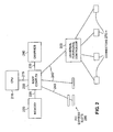
- FIG. 2 is a schematic block diagram of a computer architecture 200 incorporating features of the present invention.
- the computer architecture 200 includes a processor 210, coupled to a bridge logic device 230 via a bus 215, such as a CPU bus.
- the bridge logic device 230 is referred to as a "root complex” but may be embodied using, for example, the "North" bridge 130 of FIG. 1 .
- the root complex 230 is also coupled to a memory 220 via a bus 225, such as a memory bus, and to one or more graphics devices 240, via a bus 235.
- the computer architecture 200 includes the universal peripheral controller 300, discussed further below in conjunction with FIG. 3 .
- a PCI-Express bus 240 is employed between the root complex 230 and the universal peripheral controller 300.
- the PCI-Express standard allows the root complex 230 to connect directly to the PCI-Express slots 280 (unlike the conventional architecture that routed such communications via the South bridge 150).
- the PCI-Express standard permits trace lengths of up to 40 inches.
- the universal peripheral controller 300 connects directly to the peripheral connectors 270-n, without an intervening PHY interface 160.
- the peripheral connectors 270-n may be embodied, for example, as Ethernet connectors (such as an RJ45 connector), a wireless local area network (WLAN) connection, or USB 2.0 connectors.
- FIG. 3 is a schematic block diagram illustrating the universal peripheral controller 300 of FIG. 2 in further detail.
- the universal peripheral controller 300 includes a bus interface 310, such as a PCI-Express interface in the exemplary embodiment.
- the universal peripheral controller 300 includes a switch 320 for demultiplexing the serial communications on the PCI-Express bus 240 for routing to the appropriate peripheral device (not shown) via the corresponding connector 350-n.
- the universal peripheral controller 300 For each supported peripheral connection, the universal peripheral controller 300 includes appropriate MAC and PHY controllers 330-n, 340-n and a peripheral connector 350-n.
- the MAC controllers 330 store and forward packets to and from a network, in a known manner.
- the PHY controllers 340 provide the electrical interface onto the network (or another connection, such as a USB or Firewire connection).
- the peripheral devices that are connected to the connectors 350-n would typically include their own MAC and PHY controllers, as appropriate, in a known manner.
- the universal peripheral controller 300 supports various peripheral protocols without requiring redundant PHY controllers for each peripheral device on the motherboard.
- the universal peripheral controller 300 exhibits reduced complexity, cost and power consumption, relative to the conventional architecture 100 of FIG. 1 .
- a plurality of identical die are typically formed in a repeated pattern on a surface of the wafer.
- Each die includes a universal peripheral controller device 300 described herein, and may include other structures or circuits.
- the individual die are cut or diced from the wafer, then packaged as an integrated circuit.
- One skilled in the art would know how to dice wafers and package die to produce integrated circuits. Integrated circuits so manufactured are considered part of this invention.
Landscapes
- Engineering & Computer Science (AREA)
- Physics & Mathematics (AREA)
- General Engineering & Computer Science (AREA)
- Theoretical Computer Science (AREA)
- Mathematical Physics (AREA)
- Computer Hardware Design (AREA)
- General Physics & Mathematics (AREA)
- Information Transfer Systems (AREA)
- Bus Control (AREA)
- Multi Processors (AREA)
Description
- The present application claims priority to
United States Provisional Patent Application Serial Number 60/525,229, filed November 25, 2003 - The present invention relates generally to computing devices and, more particularly, to methods and apparatus for controlling peripheral devices.
- Computing systems include a number of internal and external components and devices that must communicate and operate in compatible manner order to perform the functions of the computing device. A typical computing environment includes components and devices manufactured by various manufacturers. Bridge logic devices are often employed to provide connectivity between the various devices in a computing system.
FIG. 1 is a schematic block diagram of the architecture of an exemplaryconventional computing system 100. As shown inFIG. 1 , a typical architecture includes a processor (CPU) 110 coupled to abridge logic device 130 via abus 115, such as a CPU bus. Thebridge logic device 130 is often referred to as a "North" bridge because it is typically depicted at the top of computer system drawings. The Northbridge 130 is also coupled to amemory 120 via abus 125, such as a memory bus, and to one ormore graphics devices 140, via abus 135. - A second
bridge logic device 150, typically referred to as a "South" bridge, is typically used to provide a standard interface to a number of peripheral devices and other devices. The South bridge 150 permits manufacturers of peripheral devices to provide devices that are compatible with computer systems of other manufacturers. The Southbridge 150 aggregates communications between the various peripheral devices and theprocessor 110. As shown inFIG. 1 , a peripheral device can be connected to thecomputer system 100 via one or more connectors 170-n to a corresponding physical interface (PHY) 160-1. through 160-N or one ormore PCI slots 180, in a well-known manner. - Supporting the peripheral devices in the manner shown in
FIG. 1 significantly contributes to the overall system cost of acomputing system 100. For example, the costs of implementing thearchitecture 100 ofFIG. 1 includes the costs of the Southbridge 150, as well asmultiple PHY interfaces 160 or Media Access Controller (MAC)/PHY devices for various peripheral devices, such as network cards, modems and Universal Serial Bus (USB 2.0) devices. - Communications between the South
bridge 150 and the Northbridge 130 are often over a parallel Peripheral Component Interconnect (PCI) bus. The shared nature of the PCI bus, however, requires that only one peripheral device can communicate on the bus at a time. Further, as additional devices are connected to the PCI bus, additional wires and routing are required. Thus, the PCI bus architecture of the South bridge is generally not scaleable as the number of connected peripheral devices increases. - A need therefore exists for a more cost effective architecture for controlling and communicating with peripheral devices. A further need exists for an integrated controller that is scaleable as the number of connected peripheral devices increases.
- Document
US 6 324 605 dicloses a switch for connecting a peripheral to a computer, the said switch having a peripheral interface to translate either USB or non-USB peripheral data to a common data format - In one aspect the invention provides an integrated controller according to
claim 1.
In another aspect the invention provides a method according to claim 6. - Generally, an integrated controller is provided for controlling communications with a plurality of peripheral devices. The integrated controller includes a bus interface for processing communications with a processor; a switch for routing communications between the processor and one or more of the peripheral devices; and a plurality of controllers, where each of the controllers provide an interface to at least one peripheral device. The controllers include at least one PHY controller for a corresponding peripheral device that provides an electrical interface to a connection, such as a network connection. The controllers also include at least one MAC controller that stores and forwards packets to and from a network connection.
- A more complete understanding of the present invention, as well as further features and advantages of the present invention, will be obtained by reference to the following detailed description and drawings.
-
-
FIG. 1 is a schematic block diagram of the architecture of an exemplary conventional computing system; -
FIG. 2 is a schematic block diagram of a computer architecture incorporating features of the present invention; and -
FIG. 3 is a schematic block diagram illustrating the universal peripheral controller ofFIG. 2 in further detail. - The present invention recognizes that System on a Chip (SoC) technology permits a number of devices to be integrated on a single chip to reduce overall system cost. The present invention also recognizes that such SoC techniques can be employed to provide a universal
peripheral controller 300 that improves the reliability and reduces the cost of supporting peripheral devices in a computing system, such as thecomputing system 100 ofFIG. 1 . - In the
conventional architecture 100 shown inFIG. 1 , theSouth bridge 150 must provide a switching function to coordinate the communications with the various peripheral devices (not shown), as well as a PHY layer interface (not shown) for each peripheral connection. Similarly, eachperipheral connector 170 must have another associated PHY interface 160 (or MAC/PHY device). As discussed hereinafter, the universalperipheral controller 300 of the present invention integrates the components that support the peripheral devices. For example, as discussed further below in conjunction withFIG. 3 , the universalperipheral controller 300 provides an interface to the North bridge 130 (or a similar device) and includes the MAC/PHY interfaces for communicating with the peripheral devices, all integrated on a single integrated circuit (IC). In this manner, the universalperipheral controller 300 eliminates the need for translation among different proprietary protocols and redundant PHY interfaces for each peripheral device, as required by theconventional architecture 100 ofFIG. 1 . In addition, the universalperipheral controller 300 demonstrates reduced complexity, cost and power consumption, relative to theconventional architecture 100. - In one exemplary implementation, the universal
peripheral controller 300 employs a PCI-Express bus architecture. For a detailed discussion of the PCI-Express bus architecture , see, for example www.pcisig.com, incorporated by reference herein. Generally, the PCI-Express bus architecture can be scaled as the number of peripheral devices increases. In addition, the PCI-Express bus provides for serial communications at a high speed, thus allowing for a smaller connector with a reduced number of pins. The original PCI specification defined a 32-bit PCI bus that operated at 33 MHz with a peak throughput of 132 Megabytes/second. Until recently, the performance of the original PCI specification was adequate for most applications. As the processing rates of commercially available processors have increased, the processing capacity of the processors to process data eventually exceeded the capacity of the PCI bus to deliver data. Thus, recent processors can process data faster than the PCI bus can deliver the data to processor. - An updated version of the PCI specification, referred to as PCI Express, proposes to improve the computer performance by increasing the flow of data between a processor and various peripheral devices, such as network cards, printers and storage disks. Rather than transmitting data on a parallel bus, which limits the maximum transmitting speed, PCI-Express uses high speed serial lanes at 2.5Gbit/second or higher to transmit the data. When multiple lanes are used, e.g., 32 lanes, the maximum speed can be up to 80Gbit/second. In addition, PCI-Express includes a number of new features that are said to improve reliability, timing and scalability of the bus.
-
FIG. 2 is a schematic block diagram of a computer architecture 200 incorporating features of the present invention. As shown inFIG. 2 , the computer architecture 200 includes aprocessor 210, coupled to abridge logic device 230 via abus 215, such as a CPU bus. Thebridge logic device 230 is referred to as a "root complex" but may be embodied using, for example, the "North"bridge 130 ofFIG. 1 . Theroot complex 230 is also coupled to amemory 220 via abus 225, such as a memory bus, and to one ormore graphics devices 240, via abus 235. - According to one aspect of the present invention, the computer architecture 200 includes the universal
peripheral controller 300, discussed further below in conjunction withFIG. 3 . In one exemplary implementation, a PCI-Express bus 240 is employed between theroot complex 230 and the universalperipheral controller 300. Among other benefits, the PCI-Express standard allows theroot complex 230 to connect directly to the PCI-Express slots 280 (unlike the conventional architecture that routed such communications via the South bridge 150). Generally, with current technologies, the PCI-Express standard permits trace lengths of up to 40 inches. - As shown in
FIG. 2 and discussed further below in conjunction withFIG. 3 , the universalperipheral controller 300 connects directly to the peripheral connectors 270-n, without an interveningPHY interface 160. The peripheral connectors 270-n may be embodied, for example, as Ethernet connectors (such as an RJ45 connector), a wireless local area network (WLAN) connection, or USB 2.0 connectors. -
FIG. 3 is a schematic block diagram illustrating the universalperipheral controller 300 ofFIG. 2 in further detail. As shown inFIG. 3 , the universalperipheral controller 300 includes abus interface 310, such as a PCI-Express interface in the exemplary embodiment. In addition, the universalperipheral controller 300 includes aswitch 320 for demultiplexing the serial communications on the PCI-Express bus 240 for routing to the appropriate peripheral device (not shown) via the corresponding connector 350-n. - For each supported peripheral connection, the universal
peripheral controller 300 includes appropriate MAC and PHY controllers 330-n, 340-n and a peripheral connector 350-n. TheMAC controllers 330 store and forward packets to and from a network, in a known manner. ThePHY controllers 340 provide the electrical interface onto the network (or another connection, such as a USB or Firewire connection). It is noted that the peripheral devices that are connected to the connectors 350-n would typically include their own MAC and PHY controllers, as appropriate, in a known manner. In this manner, the universalperipheral controller 300 supports various peripheral protocols without requiring redundant PHY controllers for each peripheral device on the motherboard. In addition, the universalperipheral controller 300 exhibits reduced complexity, cost and power consumption, relative to theconventional architecture 100 ofFIG. 1 . - When fabricating the integrated circuits incorporating the universal
peripheral controller 300 of the present invention, a plurality of identical die are typically formed in a repeated pattern on a surface of the wafer. Each die includes a universalperipheral controller device 300 described herein, and may include other structures or circuits. The individual die are cut or diced from the wafer, then packaged as an integrated circuit. One skilled in the art would know how to dice wafers and package die to produce integrated circuits. Integrated circuits so manufactured are considered part of this invention.
Claims (7)
- An integrated controller for communicating with a plurality of peripheral devices, comprising:a bus interface for processing communications with a processor,a switch for routing communications between said processor and one or more of said plurality of peripheral devices; anda plurality of controllers, each of said controllers providing an interface to at least one peripheral device.
- The integrated controller of claim 1, wherein at least one of said plurality of controllers includes a PHY controller for a corresponding peripheral device or a MAC controller for a corresponding peripheral device.
- The integrated controller of claim 1, wherein said plurality of controllers translate said communications into a format suitable for said corresponding peripheral devices.
- The integrated controller of claim 1, wherein said bus interface provides said communications to said processor via a North bridge or a South bridge.
- The integrated controller of claim 1, wherein said integrated controller is embodied on an integrated circuit or a System on a Chip.
- A method performed by an integrated device for communicating with a plurality of peripheral devices, comprising:processing communications with a processor;routing communications between said processor and one or more of said plurality of peripheral devices; andproviding an interface to said plurality of peripheral devices.
- The method of claim 6, further comprising the step of storing and forwarding packets to and from a network.
Applications Claiming Priority (4)
| Application Number | Priority Date | Filing Date | Title |
|---|---|---|---|
| US52522903P | 2003-11-25 | 2003-11-25 | |
| US525229P | 2003-11-25 | ||
| US10/880,331 US8856401B2 (en) | 2003-11-25 | 2004-06-29 | Universal controller for peripheral devices in a computing system |
| US880331 | 2004-06-29 |
Publications (3)
| Publication Number | Publication Date |
|---|---|
| EP1536343A2 EP1536343A2 (en) | 2005-06-01 |
| EP1536343A3 EP1536343A3 (en) | 2006-09-06 |
| EP1536343B1 true EP1536343B1 (en) | 2011-03-16 |
Family
ID=34468048
Family Applications (1)
| Application Number | Title | Priority Date | Filing Date |
|---|---|---|---|
| EP20040257126 Expired - Lifetime EP1536343B1 (en) | 2003-11-25 | 2004-11-17 | Universal controller for peripheral devices in a computing system |
Country Status (4)
| Country | Link |
|---|---|
| US (1) | US8856401B2 (en) |
| EP (1) | EP1536343B1 (en) |
| JP (1) | JP4800607B2 (en) |
| DE (1) | DE602004031814D1 (en) |
Families Citing this family (16)
| Publication number | Priority date | Publication date | Assignee | Title |
|---|---|---|---|---|
| KR101050584B1 (en) * | 2004-07-30 | 2011-07-19 | 삼성전자주식회사 | Apparatus and method for controlling medium access in wireless access system |
| US9274586B2 (en) * | 2004-09-08 | 2016-03-01 | Cisco Technology, Inc. | Intelligent memory interface |
| US8021193B1 (en) | 2005-04-25 | 2011-09-20 | Nvidia Corporation | Controlled impedance display adapter |
| US7793029B1 (en) * | 2005-05-17 | 2010-09-07 | Nvidia Corporation | Translation device apparatus for configuring printed circuit board connectors |
| US7698482B2 (en) * | 2005-07-08 | 2010-04-13 | Altera Corporation | Multiple data rates in integrated circuit device serial interface |
| US8234482B2 (en) * | 2005-10-13 | 2012-07-31 | Google Inc. | Universal embedded controller for freeing CPU from operations of peripheral subsystem units with table of functions including an instruction specifying battery controller select protocol |
| US7516263B2 (en) * | 2006-02-27 | 2009-04-07 | Emerson Network Power - Embedded Computing, Inc. | Re-configurable PCI-Express switching device |
| US20070260900A1 (en) * | 2006-05-03 | 2007-11-08 | Renesas Technology America, Inc. | High-performance microprocessor with lower-performance microcontroller in a vehicle network |
| US8102842B2 (en) | 2006-08-04 | 2012-01-24 | Broadcom Corporation | Integrated switch |
| CN101523364A (en) | 2006-08-18 | 2009-09-02 | Nxp股份有限公司 | MAC and PHY interface arrangement |
| DE102007054390A1 (en) * | 2006-11-15 | 2008-05-21 | Weinmann Geräte für Medizin GmbH + Co. KG | Rebreathing gas portion determining method for use in respiration gas supply system, involves determining expiration and leakage volumes, and determining difference between expiration and leakage volumes as rebreathing portion |
| US8165133B2 (en) | 2006-12-22 | 2012-04-24 | Broadcom Corporation | Physical layer device with integrated switch |
| US8041874B2 (en) * | 2008-08-08 | 2011-10-18 | Standard Microsystems Corporation | USB and ethernet controller combination device |
| JP5565141B2 (en) | 2010-06-28 | 2014-08-06 | 富士通株式会社 | Control device, switching device, optical transmission device, and control method |
| US20160217095A1 (en) * | 2015-01-22 | 2016-07-28 | Hamilton Sundstrand Corporation | Modular signal interface unit |
| US10444999B2 (en) * | 2016-10-13 | 2019-10-15 | Qualcomm Incorporated | Universal flash storage (UFS) host design for supporting embedded UFS and UFS card |
Family Cites Families (39)
| Publication number | Priority date | Publication date | Assignee | Title |
|---|---|---|---|---|
| US6658480B2 (en) * | 1997-10-14 | 2003-12-02 | Alacritech, Inc. | Intelligent network interface system and method for accelerated protocol processing |
| US6226700B1 (en) | 1998-03-13 | 2001-05-01 | Compaq Computer Corporation | Computer system with bridge logic that includes an internal modular expansion bus and a common master interface for internal master devices |
| JP3189784B2 (en) | 1998-04-23 | 2001-07-16 | 日本電気株式会社 | Layer 3 multicast transmission method |
| US6393457B1 (en) * | 1998-07-13 | 2002-05-21 | International Business Machines Corporation | Architecture and apparatus for implementing 100 Mbps and GBPS Ethernet adapters |
| US6065073A (en) * | 1998-08-17 | 2000-05-16 | Jato Technologies, Inc. | Auto-polling unit for interrupt generation in a network interface device |
| US6385211B1 (en) * | 1998-08-19 | 2002-05-07 | Intel Corporation | Network controller |
| US6421735B1 (en) * | 1998-10-30 | 2002-07-16 | Advanced Micro Devices, Inc. | Apparatus and method for automatically selecting a network port for a home network station |
| GB2361561B (en) * | 1998-11-16 | 2003-10-29 | Infineon Technologies Ag | Universal resource access controller |
| US6453370B1 (en) * | 1998-11-16 | 2002-09-17 | Infineion Technologies Ag | Using of bank tag registers to avoid a background operation collision in memory systems |
| US6363439B1 (en) | 1998-12-07 | 2002-03-26 | Compaq Computer Corporation | System and method for point-to-point serial communication between a system interface device and a bus interface device in a computer system |
| US6324605B1 (en) | 1998-12-10 | 2001-11-27 | Network Technologies, Inc. | Computer and peripheral switch with USB |
| US6141719A (en) | 1998-12-10 | 2000-10-31 | Network Technologies, Inc. | USB selector switch |
| US6678645B1 (en) * | 1999-10-28 | 2004-01-13 | Advantest Corp. | Method and apparatus for SoC design validation |
| US7065582B1 (en) * | 1999-12-21 | 2006-06-20 | Advanced Micro Devices, Inc. | Automatic generation of flow control frames |
| US6195749B1 (en) * | 2000-02-10 | 2001-02-27 | Advanced Micro Devices, Inc. | Computer system including a memory access controller for using non-system memory storage resources during system boot time |
| US6769046B2 (en) | 2000-02-14 | 2004-07-27 | Palmchip Corporation | System-resource router |
| JP4298878B2 (en) * | 2000-02-17 | 2009-07-22 | インターナショナル・ビジネス・マシーンズ・コーポレーション | Display method of power consumption information and electronic device |
| WO2001061935A1 (en) * | 2000-02-17 | 2001-08-23 | Conexant Systems, Inc, | Cable modem having a programmable media access controller |
| US6922548B1 (en) * | 2000-04-24 | 2005-07-26 | Microsoft Corporation | Providing remote network driver interface specification services over a wireless radio-frequency medium |
| WO2002017100A1 (en) * | 2000-08-24 | 2002-02-28 | 2Wire, Inc. | System and method for selectively bridging and routing data packets between multiple networks |
| US6785751B1 (en) * | 2000-09-19 | 2004-08-31 | Intel Corporation | Method and apparatus for minimizing bus contention for I/O controller write operations |
| US6647438B1 (en) * | 2000-09-19 | 2003-11-11 | Intel Corporation | Direct memory access transfer reduction method and apparatus to overlay data on to scatter gather descriptors for bus-mastering I/O controllers |
| US20020165947A1 (en) * | 2000-09-25 | 2002-11-07 | Crossbeam Systems, Inc. | Network application apparatus |
| GB2368671B (en) * | 2000-11-03 | 2004-08-18 | Advanced Risc Mach Ltd | A logic unit and integrated circuit for clearing interrupts |
| US6701406B1 (en) * | 2000-11-17 | 2004-03-02 | Advanced Micro Devices, Inc. | PCI and MII compatible home phoneline networking alliance (HPNA) interface device |
| US6947438B1 (en) * | 2000-11-17 | 2005-09-20 | Advanced Micro Devices, Inc. | PCI and MII compatible home phoneline networking alliance (HPNA) interface device |
| US7379475B2 (en) * | 2002-01-25 | 2008-05-27 | Nvidia Corporation | Communications processor |
| JP2002232978A (en) * | 2001-02-07 | 2002-08-16 | Hitachi Ltd | Remote controller for controlling device on network, converter, and control system |
| US6990108B2 (en) * | 2001-04-06 | 2006-01-24 | Texas Instruments Incorporated | ATM system architecture for the convergence of data, voice and video |
| US20020181055A1 (en) * | 2001-04-20 | 2002-12-05 | Grant Christiansen | System and method for embedding control information within an optical wireless link |
| JP2003143352A (en) | 2001-10-31 | 2003-05-16 | Canon Inc | Facsimile gateway, control method for the facsimile gateway, and control program for the facsimile gateway |
| US7209874B2 (en) * | 2002-02-25 | 2007-04-24 | Zoran Corporation | Emulator-enabled network connectivity to a device |
| US7535913B2 (en) * | 2002-03-06 | 2009-05-19 | Nvidia Corporation | Gigabit ethernet adapter supporting the iSCSI and IPSEC protocols |
| US7171505B2 (en) * | 2002-05-02 | 2007-01-30 | International Business Machines Corporation | Universal network interface connection |
| GB0211764D0 (en) * | 2002-05-22 | 2002-07-03 | 3Com Corp | Automatic power saving facility for network devices |
| US7693078B2 (en) * | 2003-11-13 | 2010-04-06 | Rumi Sheryar Gonda | Method for supporting SDH/SONET OAMP on Ethernet |
| US7793276B2 (en) * | 2003-11-14 | 2010-09-07 | Intel Corporation | Apparatus and method for automatically parallelizing network applications through pipelining transformation |
| US20050114554A1 (en) * | 2003-11-25 | 2005-05-26 | Kameran Azadet | Peripheral controller with shared EEPROM |
| US6954450B2 (en) * | 2003-11-26 | 2005-10-11 | Cisco Technology, Inc. | Method and apparatus to provide data streaming over a network connection in a wireless MAC processor |
-
2004
- 2004-06-29 US US10/880,331 patent/US8856401B2/en active Active
- 2004-11-17 DE DE200460031814 patent/DE602004031814D1/en not_active Expired - Lifetime
- 2004-11-17 EP EP20040257126 patent/EP1536343B1/en not_active Expired - Lifetime
- 2004-11-25 JP JP2004339703A patent/JP4800607B2/en not_active Expired - Fee Related
Also Published As
| Publication number | Publication date |
|---|---|
| JP2005158076A (en) | 2005-06-16 |
| DE602004031814D1 (en) | 2011-04-28 |
| EP1536343A2 (en) | 2005-06-01 |
| EP1536343A3 (en) | 2006-09-06 |
| JP4800607B2 (en) | 2011-10-26 |
| US8856401B2 (en) | 2014-10-07 |
| US20050114581A1 (en) | 2005-05-26 |
Similar Documents
| Publication | Publication Date | Title |
|---|---|---|
| EP1536343B1 (en) | Universal controller for peripheral devices in a computing system | |
| JP6400714B2 (en) | Flexible mobile device connectivity with automotive systems with USB hubs | |
| US6131125A (en) | Plug-and-play data cable with protocol translation | |
| US20150347345A1 (en) | Gen3 pci-express riser | |
| EP1684186B1 (en) | Dual PCI-X/PCI-E card | |
| KR102403627B1 (en) | Method and apparatus for supporting a field programmable gate array (fpga) based add-in-card (aic) solid state drive (ssd) | |
| US20050270298A1 (en) | Daughter card approach to employing multiple graphics cards within a system | |
| US20050138154A1 (en) | Enclosure management device | |
| US20110043989A1 (en) | Motherboard and portable electronic device using the same | |
| CN102750250A (en) | Interface device and wiring board | |
| US20140098113A1 (en) | Network-enabled graphics processing unit | |
| EP3435243B1 (en) | Extended message signaled interrupts (msi) message data | |
| US5793999A (en) | Interface unit and a computer using the interface unit | |
| CN101599050B (en) | Adaptable pci express controller core and method | |
| CN113312304B (en) | A kind of interconnection device, motherboard and server | |
| JP2000222337A (en) | Interface device | |
| US20050114554A1 (en) | Peripheral controller with shared EEPROM | |
| CN111858459B (en) | Processor and computer | |
| CN111897754B (en) | External multi-host system | |
| US20060095626A1 (en) | Multifunction adapter | |
| EP1365544B1 (en) | Bridge element enabled module and method | |
| US8935648B2 (en) | At least one die produced, at least in part, from wafer, and including at least one replicated integrated circuit | |
| JP7052929B2 (en) | Information processing device and communication switching method | |
| EP1851640A2 (en) | Scalable universal serial bus architecture | |
| CN113485957B (en) | Multi-protocol system control device and multi-protocol system control method for physical layer suitable for industrial-level application scene |
Legal Events
| Date | Code | Title | Description |
|---|---|---|---|
| PUAI | Public reference made under article 153(3) epc to a published international application that has entered the european phase |
Free format text: ORIGINAL CODE: 0009012 |
|
| AK | Designated contracting states |
Kind code of ref document: A2 Designated state(s): AT BE BG CH CY CZ DE DK EE ES FI FR GB GR HU IE IS IT LI LU MC NL PL PT RO SE SI SK TR |
|
| AX | Request for extension of the european patent |
Extension state: AL HR LT LV MK YU |
|
| PUAL | Search report despatched |
Free format text: ORIGINAL CODE: 0009013 |
|
| AK | Designated contracting states |
Kind code of ref document: A3 Designated state(s): AT BE BG CH CY CZ DE DK EE ES FI FR GB GR HU IE IS IT LI LU MC NL PL PT RO SE SI SK TR |
|
| AX | Request for extension of the european patent |
Extension state: AL HR LT LV MK YU |
|
| 17P | Request for examination filed |
Effective date: 20070228 |
|
| AKX | Designation fees paid |
Designated state(s): DE FR GB |
|
| 17Q | First examination report despatched |
Effective date: 20070509 |
|
| GRAP | Despatch of communication of intention to grant a patent |
Free format text: ORIGINAL CODE: EPIDOSNIGR1 |
|
| GRAS | Grant fee paid |
Free format text: ORIGINAL CODE: EPIDOSNIGR3 |
|
| GRAA | (expected) grant |
Free format text: ORIGINAL CODE: 0009210 |
|
| AK | Designated contracting states |
Kind code of ref document: B1 Designated state(s): DE FR GB |
|
| REG | Reference to a national code |
Ref country code: GB Ref legal event code: FG4D |
|
| REF | Corresponds to: |
Ref document number: 602004031814 Country of ref document: DE Date of ref document: 20110428 Kind code of ref document: P |
|
| REG | Reference to a national code |
Ref country code: DE Ref legal event code: R096 Ref document number: 602004031814 Country of ref document: DE Effective date: 20110428 |
|
| PLBE | No opposition filed within time limit |
Free format text: ORIGINAL CODE: 0009261 |
|
| STAA | Information on the status of an ep patent application or granted ep patent |
Free format text: STATUS: NO OPPOSITION FILED WITHIN TIME LIMIT |
|
| 26N | No opposition filed |
Effective date: 20111219 |
|
| REG | Reference to a national code |
Ref country code: DE Ref legal event code: R097 Ref document number: 602004031814 Country of ref document: DE Effective date: 20111219 |
|
| PGFP | Annual fee paid to national office [announced via postgrant information from national office to epo] |
Ref country code: FR Payment date: 20131108 Year of fee payment: 10 |
|
| REG | Reference to a national code |
Ref country code: FR Ref legal event code: ST Effective date: 20150731 |
|
| PG25 | Lapsed in a contracting state [announced via postgrant information from national office to epo] |
Ref country code: FR Free format text: LAPSE BECAUSE OF NON-PAYMENT OF DUE FEES Effective date: 20141201 |
|
| PGFP | Annual fee paid to national office [announced via postgrant information from national office to epo] |
Ref country code: GB Payment date: 20151027 Year of fee payment: 12 |
|
| REG | Reference to a national code |
Ref country code: DE Ref legal event code: R082 Ref document number: 602004031814 Country of ref document: DE Representative=s name: DILG, HAEUSLER, SCHINDELMANN PATENTANWALTSGESE, DE Ref country code: DE Ref legal event code: R082 Ref document number: 602004031814 Country of ref document: DE Representative=s name: DILG HAEUSLER SCHINDELMANN PATENTANWALTSGESELL, DE Ref country code: DE Ref legal event code: R081 Ref document number: 602004031814 Country of ref document: DE Owner name: AVAGO TECHNOLOGIES GENERAL IP (SINGAPORE) PTE., SG Free format text: FORMER OWNER: AGERE SYSTEMS, INC., ALLENTOWN, PA., US Ref country code: DE Ref legal event code: R081 Ref document number: 602004031814 Country of ref document: DE Owner name: AVAGO TECHNOLOGIES INTERNATIONAL SALES PTE. LT, SG Free format text: FORMER OWNER: AGERE SYSTEMS, INC., ALLENTOWN, PA., US |
|
| REG | Reference to a national code |
Ref country code: DE Ref legal event code: R082 Ref document number: 602004031814 Country of ref document: DE Representative=s name: DILG, HAEUSLER, SCHINDELMANN PATENTANWALTSGESE, DE Ref country code: DE Ref legal event code: R082 Ref document number: 602004031814 Country of ref document: DE Representative=s name: DILG HAEUSLER SCHINDELMANN PATENTANWALTSGESELL, DE Ref country code: DE Ref legal event code: R081 Ref document number: 602004031814 Country of ref document: DE Owner name: AVAGO TECHNOLOGIES GENERAL IP (SINGAPORE) PTE., SG Free format text: FORMER OWNER: AGERE SYSTEMS LLC (N.D.GES.D. STAATES DELAWARE), ALLENTOWN, PA., US Ref country code: DE Ref legal event code: R081 Ref document number: 602004031814 Country of ref document: DE Owner name: AVAGO TECHNOLOGIES INTERNATIONAL SALES PTE. LT, SG Free format text: FORMER OWNER: AGERE SYSTEMS LLC (N.D.GES.D. STAATES DELAWARE), ALLENTOWN, PA., US |
|
| GBPC | Gb: european patent ceased through non-payment of renewal fee |
Effective date: 20161117 |
|
| PG25 | Lapsed in a contracting state [announced via postgrant information from national office to epo] |
Ref country code: GB Free format text: LAPSE BECAUSE OF NON-PAYMENT OF DUE FEES Effective date: 20161117 |
|
| REG | Reference to a national code |
Ref country code: DE Ref legal event code: R081 Ref document number: 602004031814 Country of ref document: DE Owner name: AVAGO TECHNOLOGIES INTERNATIONAL SALES PTE. LT, SG Free format text: FORMER OWNER: AVAGO TECHNOLOGIES GENERAL IP (SINGAPORE) PTE. LTD., SINGAPORE, SG Ref country code: DE Ref legal event code: R082 Ref document number: 602004031814 Country of ref document: DE Representative=s name: DILG, HAEUSLER, SCHINDELMANN PATENTANWALTSGESE, DE Ref country code: DE Ref legal event code: R082 Ref document number: 602004031814 Country of ref document: DE Representative=s name: DILG HAEUSLER SCHINDELMANN PATENTANWALTSGESELL, DE |
|
| REG | Reference to a national code |
Ref country code: DE Ref legal event code: R008 Ref document number: 602004031814 Country of ref document: DE Ref country code: DE Ref legal event code: R039 Ref document number: 602004031814 Country of ref document: DE |
|
| PGFP | Annual fee paid to national office [announced via postgrant information from national office to epo] |
Ref country code: DE Payment date: 20220616 Year of fee payment: 19 |
|
| REG | Reference to a national code |
Ref country code: DE Ref legal event code: R042 Ref document number: 602004031814 Country of ref document: DE |
|
| PG25 | Lapsed in a contracting state [announced via postgrant information from national office to epo] |
Ref country code: DE Free format text: THE PATENT HAS BEEN ANNULLED BY A DECISION OF A NATIONAL AUTHORITY Effective date: 20230714 |