EP1684186B1 - Dual PCI-X/PCI-E card - Google Patents
Dual PCI-X/PCI-E card Download PDFInfo
- Publication number
- EP1684186B1 EP1684186B1 EP05026023A EP05026023A EP1684186B1 EP 1684186 B1 EP1684186 B1 EP 1684186B1 EP 05026023 A EP05026023 A EP 05026023A EP 05026023 A EP05026023 A EP 05026023A EP 1684186 B1 EP1684186 B1 EP 1684186B1
- Authority
- EP
- European Patent Office
- Prior art keywords
- chip
- connector
- circuit board
- bus interface
- pci
- Prior art date
- Legal status (The legal status is an assumption and is not a legal conclusion. Google has not performed a legal analysis and makes no representation as to the accuracy of the status listed.)
- Active
Links
Images


Classifications
-
- H—ELECTRICITY
- H05—ELECTRIC TECHNIQUES NOT OTHERWISE PROVIDED FOR
- H05K—PRINTED CIRCUITS; CASINGS OR CONSTRUCTIONAL DETAILS OF ELECTRIC APPARATUS; MANUFACTURE OF ASSEMBLAGES OF ELECTRICAL COMPONENTS
- H05K1/00—Printed circuits
- H05K1/02—Details
- H05K1/11—Printed elements for providing electric connections to or between printed circuits
- H05K1/117—Pads along the edge of rigid circuit boards, e.g. for pluggable connectors
-
- H—ELECTRICITY
- H05—ELECTRIC TECHNIQUES NOT OTHERWISE PROVIDED FOR
- H05K—PRINTED CIRCUITS; CASINGS OR CONSTRUCTIONAL DETAILS OF ELECTRIC APPARATUS; MANUFACTURE OF ASSEMBLAGES OF ELECTRICAL COMPONENTS
- H05K1/00—Printed circuits
- H05K1/02—Details
- H05K1/0286—Programmable, customizable or modifiable circuits
- H05K1/0295—Programmable, customizable or modifiable circuits adapted for choosing between different types or different locations of mounted components
-
- H—ELECTRICITY
- H05—ELECTRIC TECHNIQUES NOT OTHERWISE PROVIDED FOR
- H05K—PRINTED CIRCUITS; CASINGS OR CONSTRUCTIONAL DETAILS OF ELECTRIC APPARATUS; MANUFACTURE OF ASSEMBLAGES OF ELECTRICAL COMPONENTS
- H05K1/00—Printed circuits
- H05K1/18—Printed circuits structurally associated with non-printed electric components
- H05K1/181—Printed circuits structurally associated with non-printed electric components associated with surface mounted components
-
- H—ELECTRICITY
- H05—ELECTRIC TECHNIQUES NOT OTHERWISE PROVIDED FOR
- H05K—PRINTED CIRCUITS; CASINGS OR CONSTRUCTIONAL DETAILS OF ELECTRIC APPARATUS; MANUFACTURE OF ASSEMBLAGES OF ELECTRICAL COMPONENTS
- H05K2201/00—Indexing scheme relating to printed circuits covered by H05K1/00
- H05K2201/09—Shape and layout
- H05K2201/09818—Shape or layout details not covered by a single group of H05K2201/09009 - H05K2201/09809
- H05K2201/09954—More mounting possibilities, e.g. on same place of PCB, or by using different sets of edge pads
Definitions
- the invention herein relates in general to a dual bus interface printed circuit board (PCB) and more particularly to a PCB provided with both a PCI-X (Peripheral Component Interconnect - Extended) bus interface and a PCI-E (Peripheral Component Interconnect - Express) bus interface.
- PCB printed circuit board
- PCI-X Peripheral Component Interconnect - Extended
- PCI-E Peripheral Component Interconnect - Express
- PCI Peripheral Component Interconnect
- PCI-2.2 PCI-X
- PCI - Extended PCI- Extended
- the conventional PCI architecture is based on a multi-drop, parallel bus implementation, with one local bus being shared by multiple peripheral devices to communicate with the central processing unit (CPU).
- the PCI architecture solved some of the limitations of the previous bus standards such as ISA (Industry Standard Architecture) and EISA (Extended ISA), by allowing direct access of peripheral devices to the CPU.
- ISA Industry Standard Architecture
- EISA Extended ISA
- bus technology based on the conventional PCI architecture is becoming more and more a bottleneck to enhanced system performance. The main reason for that being that a shared bus technology suffers from a scalability problem, limiting the number of peripherals that can be efficiently supported by a system.
- PCI-E PCI - Express
- PCI-E architecture is based on a series of point-to-point connections, with each connection employing a packet-based transfer scheme and supporting bidirectional communication.
- PCI-E can be easily scaled from one to 32 lanes, with a single lane providing 250MB/sec of dedicated bandwidth in each direction.
- PCI-E also supports advanced power management, hot plugging, and its packet-based transfer protocol allows for time dependent data delivery and quality of service arbitration for high priority data streams.
- PCI-E clearly provides major performance improvements compared to the conventional PCI standard and its extensions (parallel PCI), serial PCI-E is not backward compatible with parallel PCI, and the shift from parallel PCI to PCI-E is likely to be a slow one. It is expected that parallel PCI will coexist in many platforms with PCI-E to support today's lower bandwidth applications, until a compelling need, such as a new form factor, causes a full migration to fully PCI-E systems.
- the present invention is directed to a PCB having multiple different bus interface connectors, and a chipset that supports the multiple bus interfaces.
- the present invention includes a dual PCI-X/PCI-E interface PCB.
- the dual interface functionality of a PCI-X/PCI-E chipset can be fully taken advantage of by the user, operating the chipset on either a PCI-X or a PCI-E bus.
- chipset fabrication costs can be reduced as well as the fabrication process simplified, by the production of a single dual bus interface PCB instead of multiple board variations to support various bus interface types.
- a circuit board assembly comprising:
- the chip or chip set supports more than one bus interface.
- the first bus connector and the second bus connector are located on opposite edges of the circuit board.
- the first bus connector and the second bus connector are located on adjacent edges of the circuit board.
- the circuit board is configured at fabrication time to enable the first bus interface connector, the second bus interface connector, or both.
- the circuit board assembly further comprises:
- the chip or chip set comprises a RAID controller.
- the first bus connector comprises a PCI-X bus interface connector
- the second bus connector comprises a PCI-E bus interface connector
- the circuit board assembly as defined in claim 1 further comprises:
- the first set of connector ports or the second set of connector ports are used to connect the RAID controller to an array of disk drives.
- the first set of connector ports and the second set of connector ports comprise SATA/SAS connector ports.
- the first bus interface connector is enabled, and the second bus interface is not enabled.
- the circuit board assembly further comprises:
- the first bus interface connector and the second bus interface connector are both enabled.
- the circuit board can be used with either the first bus interface or the second bus interface, when bus slots of the first and second interface types are available on the system whereon the circuit board is being attached.
- a selection between using the circuit board with the first bus interface to using the circuit board with the second bus interface or vice versa is made by a 180° degrees rotation of the circuit board.
- a method of fabricating a dual bus interface circuit board comprising:
- the first bus interface connector comprises a PCI-X connector and the second bus interface connector comprises a PCI-E connector.
- the chip or chip set comprises a RAID (Redundant Array of Inexpensive Disks) controller chipset.
- RAID Redundant Array of Inexpensive Disks
- the first set and second set of connector ports comprise 8 SATA/SAS connector ports.
- both the first and the second bus interface connectors are enabled, further comprising:
- the method further comprises:
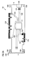
- FIG. 1A is a top view diagram of a dual-interface PCB 100.
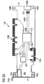
- FIG. 1B is another top view diagram of the dual-interface PCB 100.
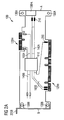
- FIG. 2A is a top view diagram of the dual-interface PCB 100 in a PCI-X configuration.
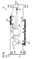
- FIG. 2B is another top view diagram of the dual-interface PCB 100 in a PCI-X configuration.
- FIG. 3A is a top view diagram of the dual-interface PCB 100 in a PCI-E configuration.
- FIG. 3B is another top view diagram of the dual-interface PCB 100 in a PCI-E configuration.
- FIG. 3C is another top view diagram of the dual-interface PCB 100 in a PCI-E configuration.
- FIG. 3D is another top view diagram of the dual-interface PCB 100 in a PCI-E configuration.
- FIG. 4 is another top view diagram of the dual-interface PCB 100.
- FIG. 5 is a side view diagram of the dual-interface PCB 100.
- FIG. 6 is a 3D view diagram of the dual-interface PCB 100.
- FIG. 1A shows a top view of an example dual-interface PCB 100 according to the present invention.
- the PCB 100 includes a main chipset 110, a first interface connector 120A, a second interface connector 120B, and two pairs of screw holes 130A and 130B located on edges A and B of the PCB 100, respectively.
- the main chipset 110 is an electronic chipset that supports two different types of bus interfaces.
- the two pairs of screw holes 130A and 130B allow the PCB 100 to be attached to a computer case from either edge A or edge B. Other attachment mechanisms can also be employed.
- the interface connectors 120A and 120B are illustrated at opposite edges of the PCB 100.
- the invention is not, however, limited to this example. Based on the description herein, one skilled in the relevant art(s) will understand that connectors 120A and 120B can be positioned on adjacent edges or on the same edge of PCB 100.
- the main chipset 110 is a RAID (Redundant Arrays of Inexpensive Disks) controller chipset.
- the interface connector 120A is a PCI-E bus interface connector.
- the interface connector 120B is a PCI-X bus interface connector.
- Connector ports 150A and 150B are placed on edge A and edge B of the PCB, respectively.
- the connector ports 150A and 150B are used to interface the RAID controller chipset 110 to an array of disk drives (not shown in the diagram).
- Signal traces 140A and 160A are routed from the main chipset 110 toward edge A of the PCB and interface connector 120A, respectively.
- signal traces 140B and 160B are routed from the main chipset 110 toward edge B of the PCB and interface connector 120B, respectively.
- Surface mount/through hole resistors can be mounted at the main chipset's ends of signal traces 140A, 140B, 160A, and 160B to connect the main chipset 110 to connector ports 150A, connector ports 150B, interface connector, 120A, and interface connector 120B, respectively.
- the PCB 100 is configured such that the interface connector 120B and connector ports 150A are enabled.
- connector ports 150A and 150B are illustrated on opposite edges of the PCB 100.
- the invention is not, however, limited to this example. Based on the description herein, one skilled in the relevant art(s) will understand that connector ports 150A and 150B can be positioned on adjacent edges or on a surface of PCB 100.
- connector ports 150A or 150B are optionally attached to the PCB at the end of the fabrication process. The PCB configuration would have been determined then, and connector ports 150A or 150B would be attached as necessary.
- each of connector ports 150A and 150B include a set of 8 SATA/SAS (Serial Advanced Technology Attachment/ Serial Attached SCSI) connector ports.
- FIG. 2A shows a top view of the dual-interface PCB 100 in a PCI-X configuration.
- Surface mount/through hole resistors 210 are mounted at the main chipset's ends of signal traces 140A to connect the main chipset 110 to connector ports 150A.
- surface mount/through hole resistors 230 are mounted at the main chipset's ends of signal traces 160B to connect the main chipset 110 to PCI-X interface connector 120B.
- a mounting bracket 220B is attached to edge B of the PCB.
- the bracket 220B allows the PCB to be fixed from edge B to a computer system's case, such that PCI-X connector 120B can be inserted into a matching PCI-X slot on the computer system's motherboard.
- the PCI-E interface connector 120A is not enabled, and no connector ports 150B are placed on edge B of the PCB. Signal traces 140B and 160A however are still laid out on the PCB.
- FIG. 2B shows another top view of the dual-interface PCB 100 in a PCI-X configuration.
- signal traces 140B are omitted from the drawing.
- a cache memory chip 240 is provided on board the PCB 100.
- Signal traces 260 connect the main chipset 110 to the memory chip 240.
- the memory chip 240 serves to improve the performance of the main chipset 110, by providing it quick access to a nearby memory cache. While a single memory chip 240 is shown in the diagram, it should be obvious to one skilled in the art that additional memory chips can also be used in this and/or other embodiments of the PCB 100.
- FIG. 3A shows a top view of the dual-interface PCB 100 in a PCI-E configuration.
- surface mount/through hole resistors 310 are mounted at the main chipset's ends of signal traces 140B to connect the main chipset 110 to connector ports 150B.
- surface mount/through hole resistors 330 are mounted at the main chipset's ends of signal traces 160A to connect the main chipset 110 to PCI-X interface connector 120A.
- a mounting bracket 220A is attached to edge A of the PCB 100.
- the bracket 220A allows the PCB to be fixed from edge A to a computer system's case, such that the PCI-E connector 120A can be inserted into a matching PCI-E slot on the computer system's motherboard.
- the PCI-X interface connector 120B is not enabled, and no connector ports 150A are placed on edge A of the PCB.
- Signal traces 140A and 160B however are still laid out on the PCB.
- FIG. 3B shows another top view of the dual-interface PCB 100 in a PCI-E configuration.
- signal traces 140A are omitted from the drawing.
- a cache memory chip 340 is provided on board the PCB 100.
- Signal traces 360 connect the main chipset 110 to the memory chip 340.
- the memory chip 340 serves to improve the performance of the main chipset 110, by providing it quick access to a nearby memory cache. While a single memory chip 340 is shown in the diagram, it should be obvious to one skilled in the art that additional memory chips can also be used in this and/or other embodiments of the PCB 100.
- FIG. 3C shows another top view of the dual-interface PCB 100 in a PCI-E configuration.
- a NIC Network Interface Card
- Signal traces 370 are routed from the main chipset 110 to the NIC chip 360.
- An Ethernet connector 380 is attached onto edge B of the PCB 100.
- the connector 380 can be, for example, an RJ45 connector.
- Signal traces 140A and 160B are omitted from the drawing for convenience.
- FIG. 3D is another top view of the dual-interface PCB 100 in a PCI-E configuration.
- the PCI-X interface connector 120B and/or the NIC chip 360 can be enabled depending on the number of I/O pins provided on the main chipset 110.
- Some of the I/O pins of the main chipset 110 can be configured to be used by either the interface connector 120B or the NIC chip 360.
- the selection of a configuration is optionally made at fabrication time through the use of surface mount/through hole resistors to enable selected traces on the PCB 100.
- FIG. 3D shows a configuration wherein signal traces 370 are enabled but signal traces 160B are not, resulting in a connected NIC chip 360 but a disconnected PCI-X bus interface 120B.
- signal traces 140A, 140B, 160A, and 160B are all enabled. As a result, in this configuration, both interface connectors 120A and 120B, as well as connector ports 150A and 150B, are operational. No mounting bracket is shown in FIG. 4 , but one can be attached to edge A and/or B of the PCB 100.
- the PCB 100 can be used with either a PCI-X or a PCI-E bus interface.
- the switching from using one interface to using the other is achieved by transferring the mounting bracket from one edge to the other, rotating the PCB 180° degrees, and plugging the desired bus interface connector into a matching bus slot on the computer system's motherboard.
- FIG. 5 shows a side view of the dual-interface PCB 100.
- connector ports 150A and 150B are attached centrally onto a surface of the PCB 100, instead of being placed on opposite edges A and B.
- the configuration frees area of the PCB 100, while still allowing an easy attachment of a matching cable at connector ports 150A and/or 150B.
- the PCB 100 is ready for use in a PCI-X configuration with the mounting brackets 220B attached to edge B of the PCB. Connector ports 150A would be used in this configuration.
- FIG. 6 shows a 3D view of the dual-interface PCB 100 mounted onto a motherboard 610 of a computer system.
- the motherboard 610 is shown provided with both a PCI-X bus slot 620 and a PCI-E bus slot 630.
- the PCB 100 is shown used in the PCI-E configuration with the PCI-E bus connector 120A connected to the PCI-E slot 630.
- Connector ports 150B are shown connected to matching SATA/SAS cables, also connected to the array of disk drives.
- the present invention puts forward a novel solution in the form of a dual interface PCB.
- the dual interface PCB of the current invention is easily configurable at fabrication time, and can support a number of different variations.
Landscapes
- Engineering & Computer Science (AREA)
- Microelectronics & Electronic Packaging (AREA)
- Combinations Of Printed Boards (AREA)
- Bus Control (AREA)
- Coupling Device And Connection With Printed Circuit (AREA)
- Credit Cards Or The Like (AREA)
Description
- The invention herein relates in general to a dual bus interface printed circuit board (PCB) and more particularly to a PCB provided with both a PCI-X (Peripheral Component Interconnect - Extended) bus interface and a PCI-E (Peripheral Component Interconnect - Express) bus interface.
- In the field of I/O Interconnect, PCI (Peripheral Component Interconnect) is a widely adopted I/O bus standard in a wide variety of computer platforms. To meet the growing demand for bandwidth by new applications, PCI has gone through several changes in the last decade leading to extension standards such as PCI-2.2 and PCI-X (PCI - Extended). These extension standards however are all built on the same architecture, protocols, signals, and connector as the conventional PCI, the reuse having been mainly supported by the combination of backward compatibility and the ease of migration from the conventional PCI to the newer standards.
- The conventional PCI architecture is based on a multi-drop, parallel bus implementation, with one local bus being shared by multiple peripheral devices to communicate with the central processing unit (CPU). When first developed, the PCI architecture solved some of the limitations of the previous bus standards such as ISA (Industry Standard Architecture) and EISA (Extended ISA), by allowing direct access of peripheral devices to the CPU. However, with the exponential growth of CPU power, bus technology based on the conventional PCI architecture is becoming more and more a bottleneck to enhanced system performance. The main reason for that being that a shared bus technology suffers from a scalability problem, limiting the number of peripherals that can be efficiently supported by a system.
- At its current state, the conventional PCI bus technology is theoretically very close to its practical limits, with only minor performance gains possible at large costs in form factor. It is for this reason therefore that the conventional PCI architecture is slowly giving way to a new standard known as the PCI-E (PCI - Express) standard.
- The PCI-E architecture is based on a series of point-to-point connections, with each connection employing a packet-based transfer scheme and supporting bidirectional communication. To meet the varying bandwidth needs of different system components, PCI-E can be easily scaled from one to 32 lanes, with a single lane providing 250MB/sec of dedicated bandwidth in each direction. In addition to providing ample bandwidth, PCI-E also supports advanced power management, hot plugging, and its packet-based transfer protocol allows for time dependent data delivery and quality of service arbitration for high priority data streams.
- Although PCI-E clearly provides major performance improvements compared to the conventional PCI standard and its extensions (parallel PCI), serial PCI-E is not backward compatible with parallel PCI, and the shift from parallel PCI to PCI-E is likely to be a slow one. It is expected that parallel PCI will coexist in many platforms with PCI-E to support today's lower bandwidth applications, until a compelling need, such as a new form factor, causes a full migration to fully PCI-E systems.
- Foreseeing the coexistence of PCI and PCI-E in future platforms, chip makers have been designing dual PCI-X/PCI-E chipsets that can be operated with either of the two bus standards. Currently available PCBs, however, are designed for use with only a single bus standard, providing a single bus connector per card. As a result, dual bus chipsets have to be mounted on multiple PCB variations to support the various bus interface types, denying the user the interface duality of the chipset component, and running higher fabrication costs to chipset manufacturers; (see e.g.
EP-A-0 356 757 ). - The likely coexistence of the PCI-X and the PCI-E bus standards in future computer platforms necessitates efficient solutions to ensure the interoperability of the two. As PCI-E is not backward compatible with the conventional PCI standard, of which PCI-X is an extension, chipset manufacturers currently resort to carrying multiple PCB variations of the same product in order to support various bus interfaces. This solution is clearly a costly and inefficient one from a fabrication process point of view.
- What is needed therefore is a dual interface PCB card that provides both PCI-X and PCI-E functionality.
- The present invention is directed to a PCB having multiple different bus interface connectors, and a chipset that supports the multiple bus interfaces. In an embodiment, the present invention includes a dual PCI-X/PCI-E interface PCB. As a result, the dual interface functionality of a PCI-X/PCI-E chipset can be fully taken advantage of by the user, operating the chipset on either a PCI-X or a PCI-E bus. Furthermore, chipset fabrication costs can be reduced as well as the fabrication process simplified, by the production of a single dual bus interface PCB instead of multiple board variations to support various bus interface types.
According to an aspect of the invention as defined in claim 1, a circuit board assembly is provided, comprising: - a circuit board;
- a first bus interface connector mounted to the circuit board, the first bus interface connector configured for a first interface protocol;
- a second bus interface connector mounted to the circuit board, the second bus interface configured for a second interface protocol; and
- an integrated circuit chip or chip set mounted to the circuit board and configured to interface with at least one of the first and second bus interface connectors;
- wherein, the chip or chip set supports more than one bus interface.
- Advantageously, the first bus connector and the second bus connector are located on opposite edges of the circuit board.
- Advantageously, the first bus connector and the second bus connector are located on adjacent edges of the circuit board.
- Advantageously, the circuit board is configured at fabrication time to enable the first bus interface connector, the second bus interface connector, or both.
- Advantageously, the circuit board assembly further comprises:
- a first set of signal traces routed from the chip or chip set to the first bus interface connector; and
- a first set of signal traces routed from the chip set to the second bus interface connector.
- Advantageously, the chip or chip set comprises a RAID controller.
- Advantageously, the first bus connector comprises a PCI-X bus interface connector, and the second bus connector comprises a PCI-E bus interface connector.
- The circuit board assembly as defined in claim 1 further comprises:
- a memory chip mounted to the circuit board, and coupled to the chip or chip set,
wherein the memory chip provides a memory cache for the chip or chip set. - a first set of connector ports coupled to the chip or chip set when the first bus interface connector is enabled; and
- a second set of connector ports coupled to the chip or chip set when the second bus interface connector is enabled; wherein, the first set of connector ports is used when the chip set is operated using the first bus interface, and the second set of connector ports is used when the chip set is operated using the second bus interface.
- Advantageously, the first set of connector ports or the second set of connector ports are used to connect the RAID controller to an array of disk drives.
- Advantageously, the first set of connector ports and the second set of connector ports comprise SATA/SAS connector ports.
- Advantageously, the first bus interface connector is enabled, and the second bus interface is not enabled.
- Advantageously, the circuit board assembly further comprises:
- a NIC (Network Interface Card) chip mounted to the circuit board, and coupled to the chip or chip set; and
- an Ethernet connector mounted to the circuit board, and coupled to the NIC chip.
- Advantageously, the first bus interface connector and the second bus interface connector are both enabled.
- In accordance with the invention as defined in claim 1, the circuit board can be used with either the first bus interface or the second bus interface, when bus slots of the first and second interface types are available on the system whereon the circuit board is being attached.
- Advantageously, a selection between using the circuit board with the first bus interface to using the circuit board with the second bus interface or vice versa, is made by a 180° degrees rotation of the circuit board.
- According to an aspect of the invention as defined in claim 9, a method of fabricating a dual bus interface circuit board is provided, comprising:
- mounting a chip or chipset on the circuit board;
- mounting a first bus interface connector and a second bus interface connector to circuit board;
- routing a first set and a second set of signal traces from the chip or chipset to the first and second bus interface connectors, respectively; and
- selectively mounting resistors at the ends of the first and/or the second set(s) of signal traces when the first and second bus interface connectors are to be enabled, respectively;
- Advantageously, the first bus interface connector comprises a PCI-X connector and the second bus interface connector comprises a PCI-E connector.
- Advantageously, the chip or chip set comprises a RAID (Redundant Array of Inexpensive Disks) controller chipset.
- Advantageously, the first set and second set of connector ports comprise 8 SATA/SAS connector ports.
- Advantageously, both the first and the second bus interface connectors are enabled, further comprising:
- attaching a first set of connector ports and a second set of connector ports onto the bottom surface of the circuit board.
- Advantageously, the method further comprises:
- drilling a screw hole at every corner of the circuit board, thereby allowing a mounting bracket to be attached at either edge of the circuit board.
- Further embodiments, features, and advantages of the present invention, as well as the structure and operation of the various embodiments of the present invention, are described in detail below with reference to the accompanying drawings.
- The accompanying drawings, which are incorporated herein and form a part of the specification, illustrate the present invention and, together with the description, further serve to explain the principles of the invention and to enable a person skilled in the pertinent art to make and use the invention.
-
FIG. 1A is a top view diagram of a dual-interface PCB 100. -
FIG. 1B is another top view diagram of the dual-interface PCB 100. -
FIG. 2A is a top view diagram of the dual-interface PCB 100 in a PCI-X configuration. -
FIG. 2B is another top view diagram of the dual-interface PCB 100 in a PCI-X configuration. -
FIG. 3A is a top view diagram of the dual-interface PCB 100 in a PCI-E configuration. -
FIG. 3B is another top view diagram of the dual-interface PCB 100 in a PCI-E configuration. -
FIG. 3C is another top view diagram of the dual-interface PCB 100 in a PCI-E configuration. -
FIG. 3D is another top view diagram of the dual-interface PCB 100 in a PCI-E configuration. -
FIG. 4 is another top view diagram of the dual-interface PCB 100. -
FIG. 5 is a side view diagram of the dual-interface PCB 100. -
FIG. 6 is a 3D view diagram of the dual-interface PCB 100. - The present invention will be described with reference to the accompanying drawings. The drawing in which an element first appears is typically indicated by the leftmost digit(s) in the corresponding reference number.
-
FIG. 1A shows a top view of an example dual-interface PCB 100 according to the present invention. In the example, thePCB 100 includes amain chipset 110, afirst interface connector 120A, asecond interface connector 120B, and two pairs ofscrew holes PCB 100, respectively. Themain chipset 110 is an electronic chipset that supports two different types of bus interfaces. The two pairs ofscrew holes PCB 100 to be attached to a computer case from either edge A or edge B. Other attachment mechanisms can also be employed. - In the example of
FIG. 1A , theinterface connectors PCB 100. The invention is not, however, limited to this example. Based on the description herein, one skilled in the relevant art(s) will understand thatconnectors PCB 100. - In another example embodiment, shown in
FIG. 1B , themain chipset 110 is a RAID (Redundant Arrays of Inexpensive Disks) controller chipset. Theinterface connector 120A is a PCI-E bus interface connector. Theinterface connector 120B is a PCI-X bus interface connector.Connector ports connector ports RAID controller chipset 110 to an array of disk drives (not shown in the diagram). Signal traces 140A and 160A are routed from themain chipset 110 toward edge A of the PCB andinterface connector 120A, respectively. Similarly, signal traces 140B and 160B are routed from themain chipset 110 toward edge B of the PCB andinterface connector 120B, respectively. Surface mount/through hole resistors can be mounted at the main chipset's ends of signal traces 140A, 140B, 160A, and 160B to connect themain chipset 110 toconnector ports 150A,connector ports 150B, interface connector, 120A, andinterface connector 120B, respectively. In the exemplary embodiment shown, thePCB 100 is configured such that theinterface connector 120B andconnector ports 150A are enabled. - In the example of
FIG. 1B ,connector ports PCB 100. The invention is not, however, limited to this example. Based on the description herein, one skilled in the relevant art(s) will understand thatconnector ports PCB 100. - In an embodiment,
connector ports connector ports connector ports -
FIG. 2A shows a top view of the dual-interface PCB 100 in a PCI-X configuration. Surface mount/throughhole resistors 210 are mounted at the main chipset's ends of signal traces 140A to connect themain chipset 110 toconnector ports 150A. Similarly, surface mount/throughhole resistors 230 are mounted at the main chipset's ends of signal traces 160B to connect themain chipset 110 to PCI-X interface connector 120B. - A mounting
bracket 220B is attached to edge B of the PCB. Thebracket 220B allows the PCB to be fixed from edge B to a computer system's case, such that PCI-X connector 120B can be inserted into a matching PCI-X slot on the computer system's motherboard. - In this example of
FIG. 2A , the PCI-E interface connector 120A is not enabled, and noconnector ports 150B are placed on edge B of the PCB. Signal traces 140B and 160A however are still laid out on the PCB. -
FIG. 2B shows another top view of the dual-interface PCB 100 in a PCI-X configuration. For ease of illustration, signal traces 140B are omitted from the drawing. Acache memory chip 240 is provided on board thePCB 100. Signal traces 260 connect themain chipset 110 to thememory chip 240. Thememory chip 240 serves to improve the performance of themain chipset 110, by providing it quick access to a nearby memory cache. While asingle memory chip 240 is shown in the diagram, it should be obvious to one skilled in the art that additional memory chips can also be used in this and/or other embodiments of thePCB 100. -
FIG. 3A shows a top view of the dual-interface PCB 100 in a PCI-E configuration. In the embodiment, surface mount/throughhole resistors 310 are mounted at the main chipset's ends of signal traces 140B to connect themain chipset 110 toconnector ports 150B. Similarly, surface mount/throughhole resistors 330 are mounted at the main chipset's ends of signal traces 160A to connect themain chipset 110 to PCI-X interface connector 120A. A mountingbracket 220A is attached to edge A of thePCB 100. Thebracket 220A allows the PCB to be fixed from edge A to a computer system's case, such that the PCI-E connector 120A can be inserted into a matching PCI-E slot on the computer system's motherboard. In this exemplary embodiment, the PCI-X interface connector 120B is not enabled, and noconnector ports 150A are placed on edge A of the PCB. Signal traces 140A and 160B however are still laid out on the PCB. -
FIG. 3B shows another top view of the dual-interface PCB 100 in a PCI-E configuration. For ease of illustration, signal traces 140A are omitted from the drawing. In this embodiment, acache memory chip 340 is provided on board thePCB 100. Signal traces 360 connect themain chipset 110 to thememory chip 340. Thememory chip 340 serves to improve the performance of themain chipset 110, by providing it quick access to a nearby memory cache. While asingle memory chip 340 is shown in the diagram, it should be obvious to one skilled in the art that additional memory chips can also be used in this and/or other embodiments of thePCB 100. -
FIG. 3C shows another top view of the dual-interface PCB 100 in a PCI-E configuration. In this embodiment, a NIC (Network Interface Card)chip 360 is provided on thePCB 100. Signal traces 370 are routed from themain chipset 110 to theNIC chip 360. AnEthernet connector 380 is attached onto edge B of thePCB 100. Theconnector 380 can be, for example, an RJ45 connector. Signal traces 140A and 160B are omitted from the drawing for convenience. -
FIG. 3D is another top view of the dual-interface PCB 100 in a PCI-E configuration. In this embodiment, depending on the number of I/O pins provided on themain chipset 110, the PCI-X interface connector 120B and/or theNIC chip 360 can be enabled. Some of the I/O pins of themain chipset 110 can be configured to be used by either theinterface connector 120B or theNIC chip 360. The selection of a configuration is optionally made at fabrication time through the use of surface mount/through hole resistors to enable selected traces on thePCB 100.FIG. 3D shows a configuration wherein signal traces 370 are enabled but signal traces 160B are not, resulting in aconnected NIC chip 360 but a disconnected PCI-X bus interface 120B. - In
FIG. 4 , signal traces 140A, 140B, 160A, and 160B are all enabled. As a result, in this configuration, bothinterface connectors connector ports FIG. 4 , but one can be attached to edge A and/or B of thePCB 100. - The
PCB 100 can be used with either a PCI-X or a PCI-E bus interface. The switching from using one interface to using the other is achieved by transferring the mounting bracket from one edge to the other, rotating the PCB 180° degrees, and plugging the desired bus interface connector into a matching bus slot on the computer system's motherboard. -
FIG. 5 shows a side view of the dual-interface PCB 100. In this embodiment,connector ports PCB 100, instead of being placed on opposite edges A and B. The configuration frees area of thePCB 100, while still allowing an easy attachment of a matching cable atconnector ports 150A and/or 150B. In the exemplary embodiment shown inFIG. 5 , thePCB 100 is ready for use in a PCI-X configuration with the mountingbrackets 220B attached to edge B of the PCB.Connector ports 150A would be used in this configuration. -
FIG. 6 shows a 3D view of the dual-interface PCB 100 mounted onto amotherboard 610 of a computer system. Themotherboard 610 is shown provided with both a PCI-X bus slot 620 and a PCI-E bus slot 630. ThePCB 100 is shown used in the PCI-E configuration with the PCI-E bus connector 120A connected to the PCI-E slot 630.Connector ports 150B are shown connected to matching SATA/SAS cables, also connected to the array of disk drives. - The present invention puts forward a novel solution in the form of a dual interface PCB. The dual interface PCB of the current invention is easily configurable at fabrication time, and can support a number of different variations.
- While the invention is described herein in view of a dual PCI-X/PCI-E interface PCB, the scope of the invention should not be limited by the type of interfaces supported by the PCB. It also should be noted that the PCB layouts provided in the accompanying drawings have been presented by way of example only, and not limitation.
- While specific configurations and arrangements are discussed, it should be understood that this is done for illustrative purposes only. A person skilled in the pertinent art will recognize that other configurations and arrangements can be used without departing from the scope of the present invention as defined by the appended claims. It will be apparent to a person skilled in the pertinent art that this invention can also be employed in a variety of other applications.
- While various embodiments of the present invention have been described above, it should be understood that they have been presented by way of example only, and not limitation. It will be apparent to persons skilled in the relevant art that various changes in form and detail can be made therein without departing from the scope of the invention as defined by the appended claims. Thus, the breadth and scope of the present invention should not be limited by any of the above-described exemplary embodiments, but should be defined only in accordance with the following claims and their equivalents.
Claims (12)
- A circuit board assembly, comprising:a circuit board;a first bus interface connector mounted to the circuit board, the first bus interface connector configured for a first interface protocol;a second bus interface connector mounted to the circuit board, the second bus interface configured for a second interface protocol; andan integrated circuit chip or chip set mounted to the circuit board and configured to interface with at least one of the first and second bus interface connectors;wherein the circuit board is insertable into a motherboard by selectively inserting either the first or the second interface connector into a corresponding slot of the motherboard; characterized in thatthe circuit board assembly further comprises at least one memory chip mounted to the circuit board, and coupled to the chip or chip set,wherein the memory chip provides a memory cache for the chip or chip set;said chip or chip set is supporting more than one bus interface; anda first set of connector ports is coupled to the chip or chip set when a first bus interface connector is enabled;a second set of connector ports is coupled to the chip or chip set when a second bus interface connector is enabled; whereinthe circuit board can be used with either the first bus interface or the second bus interface, when bus slots of the first and second interface types are available on a system whereon the circuit board is being attached.
- The circuit board assembly of claim 5, wherein the first bus connector comprises a Peripheral Component Interconnect-Extended (PCI-X) bus interface connector, and the second bus connector comprises a Peripheral Component Interconnect-Express (PCI-E) bus interface connector.
- The circuit board assembly of claim 1, wherein the circuit board is configured at fabrication time to enable the first bus interface connector, the second bus interface connector, or both.
- The circuit board assembly of claim 1, further comprising:a first set of signal traces routed from the chip or chip set to the first bus interface connector; anda second set of signal traces routed from the chip set to the second bus interface connector.
- The circuit board assembly of claim 1, wherein the first set of connector ports is used when the chip set is operated using the first bus interface, and the second set of connector ports is used when the chip set is operated using the second bus interface.
- The circuit board assembly of claim 1, further comprising:a NIC (Network Interface Card) chip mounted to the circuit board, and coupled to the chip or chip set; andan Ethernet connector mounted to the circuit board, and coupled to the NIC chip.
- The circuit board assembly of claim 1, wherein the chip or chip set comprises a RAID (Redundant Array of Inexpensive Disks) controller.
- The circuit board assembly of claim 9, wherein the first set of connector ports or the second set of connector ports are used to connect the RAID controller to an array of disk drives.
- A method of fabricating a dual bus interface circuit board, comprising:mounting a chip or chipset on the circuit board;said chip or chip set supporting more than one bus interface;mounting a first bus interface connector and a second bus interface connector to the circuit board;routing a first set and a second set of signal traces from the chip or chipset to the first and second bus interface connectors, respectively; andselectively mounting resistors at the ends of the first and/or the second set(s) of signal traces when the first and second bus interface connectors are to be enabled, respectively;wherein the circuit board is insertable into a motherboard by selectively inserting either the first or the second interface connector into a corresponding slot of the motherboard; andmounting at least one memory chip to the circuit board, and coupled to the chip or chip set,wherein the memory chip provides a memory cache for the chip or chip set;coupling a first set of connector ports to the chip or chipset when the first bus interface connector is enabled;coupling a second set of connector ports to the chip or chipset when the second bus interface connector is enabled; andusing the circuit board with either the first bus interface or the second bus interface, when bus slots of the first and second interface types are available on a system whereon the circuit board is being attached.
- The method of claim 9, wherein the first bus interface connector comprises a PCI-X connector and the second bus interface connector comprises a PCI-E connector.
- The method of claim 9, wherein the chip or chip set comprises a RAID (Redundant Array of Inexpensive Disks) controller chipset.
- The method of claim 9, wherein each of the first set and second set of connector ports comprise 8 SATA/SAS connector ports.
Applications Claiming Priority (1)
| Application Number | Priority Date | Filing Date | Title |
|---|---|---|---|
| US11/037,177 US8423695B2 (en) | 2005-01-19 | 2005-01-19 | Dual PCI-X/PCI-E card |
Publications (2)
| Publication Number | Publication Date |
|---|---|
| EP1684186A1 EP1684186A1 (en) | 2006-07-26 |
| EP1684186B1 true EP1684186B1 (en) | 2008-07-23 |
Family
ID=35636735
Family Applications (1)
| Application Number | Title | Priority Date | Filing Date |
|---|---|---|---|
| EP05026023A Active EP1684186B1 (en) | 2005-01-19 | 2005-11-29 | Dual PCI-X/PCI-E card |
Country Status (5)
| Country | Link |
|---|---|
| US (2) | US8423695B2 (en) |
| EP (1) | EP1684186B1 (en) |
| CN (1) | CN1812693B (en) |
| DE (1) | DE602005008359D1 (en) |
| TW (1) | TW200639643A (en) |
Families Citing this family (28)
| Publication number | Priority date | Publication date | Assignee | Title |
|---|---|---|---|---|
| US8423695B2 (en) * | 2005-01-19 | 2013-04-16 | Broadcom Corporation | Dual PCI-X/PCI-E card |
| DE102006005432A1 (en) * | 2006-02-07 | 2007-08-09 | Keynote Sigos Gmbh | Adapter module for preparing data link between computer and plug-in card, has power supply unit connected with function plug-in card for power supply through card interface |
| US7698488B2 (en) * | 2006-10-26 | 2010-04-13 | Hon Hai Precision Industry Co., Ltd. | Expansion apparatus for expansion card on motherboard |
| US20130107444A1 (en) * | 2011-10-28 | 2013-05-02 | Calxeda, Inc. | System and method for flexible storage and networking provisioning in large scalable processor installations |
| JP2012004423A (en) * | 2010-06-18 | 2012-01-05 | Funai Electric Co Ltd | Switch substrate and assembled substrate provided with the switch substrate |
| CN102541164A (en) * | 2010-12-14 | 2012-07-04 | 技嘉科技股份有限公司 | Computer system |
| TWM411679U (en) * | 2011-03-22 | 2011-09-11 | Tuton Technology Co Ltd | Connector expansion module implemented through PCI-E bus |
| CN102831919A (en) * | 2011-06-15 | 2012-12-19 | 鸿富锦精密工业(深圳)有限公司 | Solid state disk and mainboard for supporting same |
| CN103092737A (en) * | 2011-11-08 | 2013-05-08 | 鸿富锦精密工业(深圳)有限公司 | Computer system with solid-state hard disk rate indication function |
| CN103163974A (en) * | 2011-12-09 | 2013-06-19 | 鸿富锦精密工业(深圳)有限公司 | Solid state hard disk combination |
| CN103163987A (en) * | 2011-12-15 | 2013-06-19 | 鸿富锦精密工业(深圳)有限公司 | Solid state drive combination |
| JP6257881B2 (en) * | 2012-05-31 | 2018-01-10 | 株式会社ミクニ | Engine control unit |
| CN103365273B (en) * | 2013-07-04 | 2016-12-28 | 北京新航智科技有限公司 | A kind of master slave mode identification selection system of redundant communication module based on hardware mutex |
| CN104466578B (en) * | 2013-09-23 | 2017-06-13 | 泰州市宏祥动力机械有限公司 | With two kinds of network switch cards of network interface |
| CN104461987A (en) * | 2013-09-23 | 2015-03-25 | 鸿富锦精密电子(天津)有限公司 | Interface switching system and function card |
| US20160132454A1 (en) * | 2014-11-11 | 2016-05-12 | Allied Telesis Holdings Kabushiki Kaisha | Adapter card for thin computing devices |
| US9710421B2 (en) * | 2014-12-12 | 2017-07-18 | Intel Corporation | Peripheral component interconnect express (PCIe) card having multiple PCIe connectors |
| CN104793556B (en) * | 2015-04-15 | 2019-03-08 | 中工科安科技有限公司 | A kind of PLC design method for embedded Control of dual bus communication |
| US9407022B1 (en) * | 2015-08-14 | 2016-08-02 | Amphenol East Asia Electronic Technology (Shen Zhen) Co., Ltd. | Unitary interface used for PCI-E SAS |
| CA169446S (en) * | 2016-01-22 | 2017-02-21 | Shenzhen Longsys Electronics Co Ltd | Ssd storage module |
| US10701800B2 (en) | 2016-01-28 | 2020-06-30 | Hewlett Packard Enterprise Development Lp | Printed circuit boards |
| KR20180095765A (en) | 2017-02-17 | 2018-08-28 | 삼성전자주식회사 | Storage device and operating method of storage device |
| TWI645623B (en) * | 2017-09-30 | 2018-12-21 | 慧榮科技股份有限公司 | Memory device |
| CN108804360A (en) * | 2018-05-21 | 2018-11-13 | 郑州云海信息技术有限公司 | A kind of storage card of compatible SAS/SATA/NVME hard disks |
| CN110740569A (en) * | 2018-07-19 | 2020-01-31 | 鸿富锦精密工业(武汉)有限公司 | Printed circuit board |
| CN109783280A (en) * | 2019-01-15 | 2019-05-21 | 上海海得控制系统股份有限公司 | Shared memory systems and shared storage method |
| US11710918B2 (en) * | 2020-06-19 | 2023-07-25 | Te Connectivity Solutions Gmbh | Cable receptacle connector for a communication system |
| CN113078527A (en) * | 2021-03-10 | 2021-07-06 | 东莞立讯技术有限公司 | Adapter circuit board, first connector and connector assembly |
Family Cites Families (25)
| Publication number | Priority date | Publication date | Assignee | Title |
|---|---|---|---|---|
| US4795602A (en) * | 1986-03-19 | 1989-01-03 | Pretchel David A | Two pin shunt and molding method |
| US4885482A (en) * | 1988-07-13 | 1989-12-05 | Compaq Computer Corporation | Multiple computer interface circuit board |
| BE1002392A4 (en) | 1988-09-02 | 1991-01-22 | Devlonics Terminals N V | COMPUTER EXPANSION CARD SUITABLE FOR TWO TYPES OF COMPUTERS. |
| US5162675A (en) * | 1989-04-14 | 1992-11-10 | Digital Communications Associates, Inc. | Dual personal computer architecture peripheral adapter board and circuit |
| US5162979A (en) * | 1989-10-23 | 1992-11-10 | International Business Machines Corp. | Personal computer processor card interconnect system |
| US5189598A (en) * | 1990-08-14 | 1993-02-23 | Dallas Semiconductor Corporation | Dual function microboard with a row of connectors on two edges |
| US5169337A (en) * | 1991-09-05 | 1992-12-08 | Amp Incorporated | Electrical shunt |
| US5359728A (en) * | 1992-04-09 | 1994-10-25 | Hewlett-Packard Company | Data integrity assurance in a disk drive upon a power failure |
| US5444856A (en) * | 1992-07-07 | 1995-08-22 | Intel Corporation | Apparatus and method for switching ethernet media type |
| DE9211227U1 (en) | 1992-08-21 | 1992-12-24 | Elsa Ges. Fuer Elektronische Systeme Mbh, 5100 Aachen, De | |
| JP3237968B2 (en) * | 1993-08-18 | 2001-12-10 | 富士通株式会社 | Semiconductor element module |
| US5781747A (en) * | 1995-11-14 | 1998-07-14 | Mesa Ridge Technologies, Inc. | Method and apparatus for extending the signal path of a peripheral component interconnect bus to a remote location |
| US6036534A (en) * | 1997-02-26 | 2000-03-14 | 3M Innovative Properties Company | Low profile shunt connector |
| JPH11259605A (en) * | 1998-01-08 | 1999-09-24 | Tdk Corp | Pc card |
| US6111757A (en) * | 1998-01-16 | 2000-08-29 | International Business Machines Corp. | SIMM/DIMM memory module |
| US6434157B1 (en) * | 1998-10-06 | 2002-08-13 | Schneider Automation, Inc. | MODBUS plus ethernet bridge |
| US6142357A (en) * | 1998-10-15 | 2000-11-07 | Mcms, Inc. | Molded selective solder pallet |
| US6146150A (en) * | 1998-11-24 | 2000-11-14 | International Business Machines Corporation | Circuit card with separate interfaces for different bus architectures |
| US6301121B1 (en) * | 1999-04-05 | 2001-10-09 | Paul T. Lin | Direct-chip-attach (DCA) multiple chip module (MCM) with repair-chip ready site to simplify assembling and testing process |
| US6343007B1 (en) * | 2000-03-31 | 2002-01-29 | Alcatel Usa Sourcing, L.P. | System and method for providing system functions in a telecommunications network |
| US7051134B2 (en) * | 2003-01-21 | 2006-05-23 | Ali Corporation | Daisy chained ATA host controllers in a single PCI device |
| US7535718B2 (en) * | 2003-08-20 | 2009-05-19 | Imation Corp. | Memory card compatible with multiple connector standards |
| US20050042931A1 (en) * | 2003-08-20 | 2005-02-24 | Reuven Lavie | Reducing cross talk at ethernet connectors |
| US20060112197A1 (en) * | 2004-11-24 | 2006-05-25 | Li-Ho Yao | Dual-interface-plug memory card |
| US8423695B2 (en) * | 2005-01-19 | 2013-04-16 | Broadcom Corporation | Dual PCI-X/PCI-E card |
-
2005
- 2005-01-19 US US11/037,177 patent/US8423695B2/en active Active
- 2005-11-29 DE DE602005008359T patent/DE602005008359D1/en active Active
- 2005-11-29 EP EP05026023A patent/EP1684186B1/en active Active
-
2006
- 2006-01-13 CN CN2006100059867A patent/CN1812693B/en not_active Expired - Fee Related
- 2006-01-18 TW TW095101910A patent/TW200639643A/en unknown
-
2012
- 2012-09-14 US US13/618,247 patent/US20130080675A1/en not_active Abandoned
Also Published As
| Publication number | Publication date |
|---|---|
| EP1684186A1 (en) | 2006-07-26 |
| US20060161717A1 (en) | 2006-07-20 |
| CN1812693B (en) | 2010-11-24 |
| US20130080675A1 (en) | 2013-03-28 |
| US8423695B2 (en) | 2013-04-16 |
| TW200639643A (en) | 2006-11-16 |
| CN1812693A (en) | 2006-08-02 |
| DE602005008359D1 (en) | 2008-09-04 |
Similar Documents
| Publication | Publication Date | Title |
|---|---|---|
| EP1684186B1 (en) | Dual PCI-X/PCI-E card | |
| US6731515B2 (en) | Riser assembly and method for coupling peripheral cards to a motherboard | |
| US7246190B2 (en) | Method and apparatus for bringing bus lanes in a computer system using a jumper board | |
| CA1327410C (en) | Dual personal computer architecture peripheral adapter board and circuit | |
| US10817443B2 (en) | Configurable interface card | |
| US6735660B1 (en) | Sideband signal transmission between host and input/output adapter | |
| US7596649B2 (en) | Motherboard | |
| US20050270298A1 (en) | Daughter card approach to employing multiple graphics cards within a system | |
| US6477603B1 (en) | Multiple PCI adapters within single PCI slot on an matax planar | |
| US20070079041A1 (en) | Multiprocessor system | |
| CN107408095B (en) | Redirection of channel resources | |
| US7632139B2 (en) | Connector having USB and eSATA interfaces | |
| US20070032100A1 (en) | Replaceable input/output interface for circuit board | |
| US7612631B2 (en) | Motherboard | |
| JP4800607B2 (en) | Universal controller for peripheral devices in computing systems | |
| CN110554983A (en) | Exchange circuit board | |
| US10248605B2 (en) | Bidirectional lane routing | |
| CN213276461U (en) | Double-circuit server mainboard and server | |
| US10606792B2 (en) | Interface arrangement on a system board and computer system | |
| TWI762685B (en) | Printed circuit board | |
| KR100499585B1 (en) | Union type main board | |
| CN211787077U (en) | PCI-E switching device based on 2U server, 2U server | |
| CN100351734C (en) | Mainboard and PCI Express x16 slot thereof | |
| JP2008171291A (en) | Wiring method corresponding to high-speed serial interface | |
| KR200239759Y1 (en) | Union type main board |
Legal Events
| Date | Code | Title | Description |
|---|---|---|---|
| PUAI | Public reference made under article 153(3) epc to a published international application that has entered the european phase |
Free format text: ORIGINAL CODE: 0009012 |
|
| AK | Designated contracting states |
Kind code of ref document: A1 Designated state(s): AT BE BG CH CY CZ DE DK EE ES FI FR GB GR HU IE IS IT LI LT LU LV MC NL PL PT RO SE SI SK TR |
|
| AX | Request for extension of the european patent |
Extension state: AL BA HR MK YU |
|
| 17P | Request for examination filed |
Effective date: 20070126 |
|
| 17Q | First examination report despatched |
Effective date: 20070222 |
|
| AKX | Designation fees paid |
Designated state(s): DE FR GB |
|
| RAP1 | Party data changed (applicant data changed or rights of an application transferred) |
Owner name: BROADCOM CORPORATION |
|
| 17Q | First examination report despatched |
Effective date: 20070222 |
|
| GRAP | Despatch of communication of intention to grant a patent |
Free format text: ORIGINAL CODE: EPIDOSNIGR1 |
|
| GRAS | Grant fee paid |
Free format text: ORIGINAL CODE: EPIDOSNIGR3 |
|
| GRAA | (expected) grant |
Free format text: ORIGINAL CODE: 0009210 |
|
| AK | Designated contracting states |
Kind code of ref document: B1 Designated state(s): DE FR GB |
|
| REG | Reference to a national code |
Ref country code: GB Ref legal event code: FG4D |
|
| REF | Corresponds to: |
Ref document number: 602005008359 Country of ref document: DE Date of ref document: 20080904 Kind code of ref document: P |
|
| PLBE | No opposition filed within time limit |
Free format text: ORIGINAL CODE: 0009261 |
|
| STAA | Information on the status of an ep patent application or granted ep patent |
Free format text: STATUS: NO OPPOSITION FILED WITHIN TIME LIMIT |
|
| 26N | No opposition filed |
Effective date: 20090424 |
|
| REG | Reference to a national code |
Ref country code: FR Ref legal event code: ST Effective date: 20090731 |
|
| PG25 | Lapsed in a contracting state [announced via postgrant information from national office to epo] |
Ref country code: FR Free format text: LAPSE BECAUSE OF NON-PAYMENT OF DUE FEES Effective date: 20081130 |
|
| REG | Reference to a national code |
Ref country code: DE Ref legal event code: R082 Ref document number: 602005008359 Country of ref document: DE Representative=s name: BOSCH JEHLE PATENTANWALTSGESELLSCHAFT MBH, DE Ref country code: DE Ref legal event code: R081 Ref document number: 602005008359 Country of ref document: DE Owner name: AVAGO TECHNOLOGIES INTERNATIONAL SALES PTE. LT, SG Free format text: FORMER OWNER: BROADCOM CORP., IRVINE, CALIF., US Ref country code: DE Ref legal event code: R081 Ref document number: 602005008359 Country of ref document: DE Owner name: AVAGO TECHNOLOGIES GENERAL IP (SINGAPORE) PTE., SG Free format text: FORMER OWNER: BROADCOM CORP., IRVINE, CALIF., US |
|
| REG | Reference to a national code |
Ref country code: GB Ref legal event code: 732E Free format text: REGISTERED BETWEEN 20171005 AND 20171011 |
|
| REG | Reference to a national code |
Ref country code: DE Ref legal event code: R082 Ref document number: 602005008359 Country of ref document: DE Representative=s name: BOSCH JEHLE PATENTANWALTSGESELLSCHAFT MBH, DE Ref country code: DE Ref legal event code: R081 Ref document number: 602005008359 Country of ref document: DE Owner name: AVAGO TECHNOLOGIES INTERNATIONAL SALES PTE. LT, SG Free format text: FORMER OWNER: AVAGO TECHNOLOGIES GENERAL IP (SINGAPORE) PTE. LTD., SINGAPORE, SG |
|
| REG | Reference to a national code |
Ref country code: GB Ref legal event code: 732E Free format text: REGISTERED BETWEEN 20190222 AND 20190227 |
|
| PGFP | Annual fee paid to national office [announced via postgrant information from national office to epo] |
Ref country code: GB Payment date: 20211020 Year of fee payment: 17 |
|
| PGFP | Annual fee paid to national office [announced via postgrant information from national office to epo] |
Ref country code: DE Payment date: 20220616 Year of fee payment: 18 |
|
| GBPC | Gb: european patent ceased through non-payment of renewal fee |
Effective date: 20221129 |
|
| PG25 | Lapsed in a contracting state [announced via postgrant information from national office to epo] |
Ref country code: GB Free format text: LAPSE BECAUSE OF NON-PAYMENT OF DUE FEES Effective date: 20221129 |