EP1533903A2 - Schaltungsanordnung und Verfahren zur potentialgetrennten Übertragung einer Schaltinformation - Google Patents
Schaltungsanordnung und Verfahren zur potentialgetrennten Übertragung einer Schaltinformation Download PDFInfo
- Publication number
- EP1533903A2 EP1533903A2 EP04024121A EP04024121A EP1533903A2 EP 1533903 A2 EP1533903 A2 EP 1533903A2 EP 04024121 A EP04024121 A EP 04024121A EP 04024121 A EP04024121 A EP 04024121A EP 1533903 A2 EP1533903 A2 EP 1533903A2
- Authority
- EP
- European Patent Office
- Prior art keywords
- winding
- transformer
- voltage
- input
- circuit arrangement
- Prior art date
- Legal status (The legal status is an assumption and is not a legal conclusion. Google has not performed a legal analysis and makes no representation as to the accuracy of the status listed.)
- Granted
Links
Images


Classifications
-
- H—ELECTRICITY
- H03—ELECTRONIC CIRCUITRY
- H03K—PULSE TECHNIQUE
- H03K17/00—Electronic switching or gating, i.e. not by contact-making and –breaking
- H03K17/18—Modifications for indicating state of switch
-
- H—ELECTRICITY
- H03—ELECTRONIC CIRCUITRY
- H03K—PULSE TECHNIQUE
- H03K17/00—Electronic switching or gating, i.e. not by contact-making and –breaking
- H03K17/08—Modifications for protecting switching circuit against overcurrent or overvoltage
- H03K17/082—Modifications for protecting switching circuit against overcurrent or overvoltage by feedback from the output to the control circuit
- H03K17/0822—Modifications for protecting switching circuit against overcurrent or overvoltage by feedback from the output to the control circuit in field-effect transistor switches
-
- H—ELECTRICITY
- H03—ELECTRONIC CIRCUITRY
- H03K—PULSE TECHNIQUE
- H03K17/00—Electronic switching or gating, i.e. not by contact-making and –breaking
- H03K17/51—Electronic switching or gating, i.e. not by contact-making and –breaking characterised by the components used
- H03K17/56—Electronic switching or gating, i.e. not by contact-making and –breaking characterised by the components used by the use, as active elements, of semiconductor devices
- H03K17/60—Electronic switching or gating, i.e. not by contact-making and –breaking characterised by the components used by the use, as active elements, of semiconductor devices the devices being bipolar transistors
- H03K17/605—Electronic switching or gating, i.e. not by contact-making and –breaking characterised by the components used by the use, as active elements, of semiconductor devices the devices being bipolar transistors with galvanic isolation between the control circuit and the output circuit
- H03K17/61—Electronic switching or gating, i.e. not by contact-making and –breaking characterised by the components used by the use, as active elements, of semiconductor devices the devices being bipolar transistors with galvanic isolation between the control circuit and the output circuit using transformer coupling
-
- H—ELECTRICITY
- H03—ELECTRONIC CIRCUITRY
- H03K—PULSE TECHNIQUE
- H03K17/00—Electronic switching or gating, i.e. not by contact-making and –breaking
- H03K17/51—Electronic switching or gating, i.e. not by contact-making and –breaking characterised by the components used
- H03K17/56—Electronic switching or gating, i.e. not by contact-making and –breaking characterised by the components used by the use, as active elements, of semiconductor devices
- H03K17/687—Electronic switching or gating, i.e. not by contact-making and –breaking characterised by the components used by the use, as active elements, of semiconductor devices the devices being field-effect transistors
- H03K17/689—Electronic switching or gating, i.e. not by contact-making and –breaking characterised by the components used by the use, as active elements, of semiconductor devices the devices being field-effect transistors with galvanic isolation between the control circuit and the output circuit
- H03K17/691—Electronic switching or gating, i.e. not by contact-making and –breaking characterised by the components used by the use, as active elements, of semiconductor devices the devices being field-effect transistors with galvanic isolation between the control circuit and the output circuit using transformer coupling
Definitions
- the invention describes a circuit arrangement and an associated method for securely transmitting switching information from a first page of a Circuit arrangement for a second side of the circuit arrangement via a Potential separation away.
- Such circuit arrangements are exemplified in the control of Power semiconductor switches in modern power semiconductor modules Voltage classes of more than 600V application.
- a external control circuit the individual, preferably in half-bridge topology arranged, power semiconductor switch controlled.
- At least one of the two Power semiconductor switch such a half-bridge is on a comparison to the external control circuit different and / or varying potential.
- to Transmission of the switching signals from the primary side or the external control circuit to the secondary side are exemplified in the associated driver circuits Transformers used.
- Furthermore, in such circuit arrangements must Secondary side to be powered. Another requirement for such Circuit arrangements is that from the secondary side to the primary side error signals can be transmitted.
- US 5,900,683 discloses the transmission of both states of the drive signal by means of a transformer.
- a first transmitted frequency as "Power semiconductor switch on”
- a second transmitted frequency as “Power semiconductor switch off” interpreted on the secondary side.
- the disadvantage here is that an error feedback by means of this circuit arrangement is not possible.
- the present invention has the object of a flexibly expandable Circuitry and an associated equally flexible expandable method for secure transmission of switching information from a first side of the Circuit arrangement for a second side of the circuit arrangement via a To present potential separation.
- the input switching signal for exemplary control of a Power semiconductor switch lies on the first side, the primary side, the Circuit arrangement. It is exemplified by an external control circuit educated.
- this input switching signal divided into two paths, of which the first path is a first bidirectional switch and the second path after an inversion of the input switching signal a second bidirectional switch controls.
- a first pole of an AC voltage source preferably with a rectangular output signal, is connected to the first winding of the primary side of the Connected transformer.
- the center tap between this first and the second Winding is connected to the first switch and this is in turn to the second Pol the power source connected.
- the second winding of the primary side of the transformer is connected to the second switch and this is also connected to the second pole Voltage source connected.
- the secondary side of the transformer has a winding, which preferably with the inputs of a rectifier on the second side, the secondary side, the Circuit arrangement is connected.
- the positive output of the rectifier forms the Output switching signal.
- the operation of an above-mentioned circuit arrangement will be described in the following Description of the method for transmitting a switching information via a Potential separation outlined.
- the formed by an external control circuit preferably digital input switching signal is divided into two paths.
- the first path controls a first bidirectional switch
- the second path controls with the inverted one Signal a second bidirectional switch.
- the second switch When the first switch is closed, the second switch is open, and the first one Winding of the primary side of the transformer is with the two poles of AC voltage source connected. The second winding is not here current flowing through it.
- the first switch When the second switch is closed, the first switch is open, and the series connection of the first and the second winding of the primary side of a Transformer is connected to the poles of the AC voltage source.
- the Secondary side of the circuit On the Secondary side of the circuit is the output AC voltage from the secondary-side winding of the transformer by means of a rectifier in one DC voltage converted.
- a closed first switch now causes depending on the ratio of Winding numbers of the first primary winding and the secondary winding a first AC voltage having a first amplitude at the outputs of the secondary winding or a first DC voltage value at the output of the rectifier. This matches with advantageously the drive signal "power semiconductor switch on”.
- a closed one second switch now causes depending on the ratio of the sum of the winding numbers of first and second primary windings and the winding number of the secondary winding a second alternating voltage having a second amplitude at the outputs of secondary winding or a second DC voltage value at the output of the Rectifier. This advantageously corresponds to the drive signal "Power semiconductor switch off”.
- the output of the secondary winding of the Transformer a different amplitude, as well as the DC voltage value different values of the voltage after the rectifier.
- These different Amplitude or the different voltage value serve as Zurschaltsignal and control the two switching states of a power semiconductor switch by way of example.
- An advantage of the circuit arrangement according to the invention is that through the given configuration in addition to a switching information in addition also energy from the Primary side can be transferred to the secondary side without the described Change circuit arrangement.
- the output of the rectifier is exemplary converted into a constant supply voltage with an up-converter.
- the Output switching signal is of course before this up-converter tapped.
- the circuit arrangement for transmitting a Error signal from the secondary side can serve to the primary side. This will be on the Secondary side a controlled by an error signal located there switch between the Outputs of the rectifier switched. Furthermore, on the primary side, the second Winding of the transformer connected to the input of a threshold detector circuit. The output of the threshold detector circuit is inverted to the second input of a AND gate created. Its first input forms the input switching signal. Of the Output of the AND gate controls, as mentioned above, the two bidirectional switches.
- the error signal closes on the secondary side by means of the local switch secondary-side winding of the transformer short. This causes a on the primary side Voltage drop over the two windings. This voltage dip is by means of the threshold detector circuit detects and from this becomes a primary-side error signal educated.
- the error signal is sent to the external control circuit as well as inverted to the AND gate applied.
- An input switching signal "power semiconductor switch on” may be AND gates only pass as such when the primary-side error signal is "LOW" level having.
- Fig. 1 shows an embodiment of a circuit arrangement according to the invention. Shown is a transformer (10), wherein on its primary side two windings (12, 14) are provided. These two windings are connected in series and have a center tap.
- the transformer for transmitting a switching information via a Potential separation also has a secondary-side winding (16).
- the input switching signal (102) of the circuit arrangement for controlling a Power semiconductor switch in a power semiconductor module, not shown, is present the primary side of the circuit arrangement.
- This input switch signal (102) is in two Split paths, wherein in the first path by means of a first buffer IC (42) a first bi-directional switch (32) controls and in the second path after an inversion in one second buffer IC (44) drives a second bidirectional switch (34).
- the bidirectional switches are each as a parallel connection of each of an n-channel and a p-channel MOS FETs formed.
- a closed first switch (32) corresponds to one "HIGH" level of the input switching signal (102)
- a closed second switch (34) corresponds to a "LOW" level of the input switching signal (102).
- a first pole of an AC voltage source (20) with a rectangular Output signal is connected to the first winding (12) of the primary side of the transformer (10) connected.
- the center tap between this first (12) and the second winding (14) is connected to the first switch (32) and this in turn with the second pole of Voltage source (20) connected.
- the second winding (14) of the primary side of the transformer (10) is connected to the second switch (34) and this is also connected to the second Pol the voltage source (20) connected.
- the secondary side of the transformer (10) has a winding (16), which with the Inputs of a rectifier (50) on the secondary side of the circuit connected is.
- the first output of the rectifier forms the output switching signal (104).
- Fig. 2 shows an extended embodiment of the invention Circuit arrangement according to FIG. 1 with output circuit.
- This output circuit on the one hand serves to detect the output switching signal (104) and on the other hand to form a power supply of the secondary side.
- the output switching signal (104) via a resistor (1041) to the first input of a comparator (1045) created. Furthermore, the output switching signal (104) is passed through the center of a Voltage divider formed by a resistor (1042) and a Zener diode (1043) with parallel connected capacitor (1044), to the second input of the comparator (1045) created.
- This path forms a reference voltage, by means of which the value of the Output signal (104) can be determined. Is the value of the output signal (104) below the threshold, switch (34) is closed, is located at the output of the comparator (1045) "LOW" level and the downstream power semiconductor switch is open. Lies the value of the output signal (104) above the threshold, switch (32) is closed, the downstream power semiconductor switch is closed.
- the secondary side is the Boost converter (1123), before its inputs, a capacitor (1122) for smoothing and a coil (1121) is connected.
- the coil (1121) serves to decouple the Output switching signal (104) from the inputs of the boost converter (1123).
- the Outputs of the boost converter (1123) thus provide a constant voltage source DC voltage.
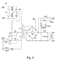
- Fig. 3 also shows an extended embodiment of the invention Circuit arrangement according to Fig. 1 with error feedback circuit and a Configuration of the AC voltage source (20).
- the AC voltage source (20) consists of two DC voltage inputs (202, 204) on an oscillator (22), the one Half-bridge arrangement of two MOS-FETs supplied from the DC voltage inputs (24, 26) controls. Their center tap forms a first pole of the AC voltage source.
- two series-connected capacitors (28) are also with the DC voltage inputs (202, 204) connected. Their center tap forms the second pole the AC voltage source.
- This circuit generates at its poles a rectangular AC voltage of the oscillator (22) adjustable frequency.
- the rectifier (50) on the secondary side has a switch (152) for connection its two outputs on each other. This switch (152) is indicated by the error signal (150) activated.
- the second winding (14) of the transformer with the Input of a threshold detector circuit (154) connected.
- These Threshold Detector Circuit (154) further includes a synchronization input (1542). which is connected to the input control signal (102).
- the exit, a primary-sided Error signal (1541) is with both the external control circuit and the second one Input of an AND gate (156) connected. Before this input becomes the error signal inverted.
- the first input of the AND gate (156) forms the input control signal (102) itself.
- the output of the AND gate becomes two paths as described under FIG split and controls the two bidirectional switches (32, 34).
- An error signal (150) closes the switch (152) between the two outputs of the rectifier (50) shorting the secondary winding (16).
- This Short circuit of the secondary winding (16) leads to a primary side Voltage reduction detected by a threshold circuit (154).
- the Threshold circuit (154) has a synchronization input (1542) connected to the Input control signal (102) is connected.
- the circuit generates only one Error signal when a drive signal "power semiconductor switch on" is present. Since that Error signal is inverted on the second input of the AND gate (156) can, a Drive signal "power semiconductor switch on” pass this AND gate (156) only if there is no error on the secondary side, so there the switch (152) is open.
- Fig. 4 shows the levels of various signals of the invention Circuit arrangement in normal operation.
- the signal (200) is that of the AC voltage source (20) generated square wave signal.
- the input control signal (102) of LOW level ("power semiconductor switch off") on HIGH level (“power semiconductor switch on”).
- the in the secondary-side winding (16) induced voltage (160) has a first value of Amplitude, since both primary-side windings (12, 14) are current-carrying.
- the change of the drive signal (102) to HIGH level causes only the more first winding (12) is flowed through current. Due to the now smaller number of Current-carrying windings on the primary side rises on the secondary side Amplitude of the induced voltage (160) through the associated winding (16). These greater amplitude is converted into an output control signal (104) by means of the rectifier (50) converted, which has an analog behavior to the input control signal (102).
- One Change at time (t2) back to a LOW level of the input control signal (102) causes an analog behavior of the output control signal (104).
- Fig. 5 shows the levels of various signals of the invention Circuit arrangement in case of error.
- the signal (200) is again that of the AC voltage source (20) generated square wave signal.
- the input control signal (102) of LOW level ("power semiconductor switch off") on HIGH level ("power semiconductor switch on") and at a later time (t2) back to LOW level.
- a time (t3) now enters on the secondary side Error signal (150) closing the associated switch (152).
- the threshold circuit (154) After the transfer on the primary side and the detection in the threshold circuit (154) generates this primary-side error signal (1541). This is due to the synchronization of Threshold circuit (154) with the input control signal (150) until the Input control signal (102) is no longer applied, regardless of whether the secondary side Error signal (150) is still present.
- the amplitude of the voltage (160) induced in the secondary-side winding (16) has a first value until time (t1). At the time (t1) at which the When the input control signal changes from LOW to HIGH level, the amplitude also changes (16) their value. At the onset of the error signal at time (t3), the amplitude changes to the lower value, since the second input of the AND gate from this Time after its inversion has a LOW level. The output control signal changes from the time (t3) to the value of the "power semiconductor switch off" equivalent. Thus, a protective function of the power semiconductor switch is given.
Landscapes
- Engineering & Computer Science (AREA)
- Power Engineering (AREA)
- Dc-Dc Converters (AREA)
- Transmitters (AREA)
- Dc Digital Transmission (AREA)
- Electronic Switches (AREA)
- Near-Field Transmission Systems (AREA)
- Time-Division Multiplex Systems (AREA)
- Cable Transmission Systems, Equalization Of Radio And Reduction Of Echo (AREA)
- Coils Or Transformers For Communication (AREA)
Abstract
Description
- Fig. 1
- zeigt eine Ausgestaltung einer erfindungsgemäßen Schaltungsanordnung.
- Fig. 2
- zeigt eine erweiterte Ausgestaltung der erfindungsgemäßen Schaltungsanordnung nach Fig. 1 mit Ausgangsbeschaltung.
- Fig. 3
- zeigt ebenfalls eine erweiterte Ausgestaltung der erfindungsgemäßen Schaltungsanordnung nach Fig. 1 mit Fehlerrückmeldungsschaltung.
- Fig. 4
- zeigt die Pegel verschiedener Signale der erfindungsgemäßen Schaltungsanordnung im Normalbetrieb.
- Fig. 5
- zeigt die Pegel verschiedener Signale der erfindungsgemäßen Schaltungsanordnung im Fehlerfall.
Claims (8)
- Schaltungsanordnung zur Übertragung einer Schaltinformation über eine Potentialtrennung hinweg, wobei das Eingangsschaltsignal (102) auf der ersten Seite, der Primärseite, der Schaltungsanordnung in zwei Pfade aufgeteilt wird, der erste Pfad einen ersten bidirektionalen Schalter (32) ansteuert und der zweite Pfad nach einer Invertierung des Eingangsschaltsignals einen zweiten bidirektionalen Schalter (34) ansteuert,
eine Wechselspannungsquelle (20) mit einem ersten Pol mit einer ersten Wicklung (12) der Primärseite eines Übertragers (10) verbunden ist, diese erste Wicklung (12) weiterhin mit der zweiten Wicklung (14) des Übertragers (10) verbunden ist und
die erste Wicklung (12) weiterhin mit dem ersten Schalter (32) und dieser wiederum mit dem zweiten Pol der Spannungsquelle (20) verbunden ist,
sowie die zweite Wicklung (14) mit dem zweiten Schalter (34) und dieser ebenfalls mit dem zweiten Pol der Spannungsquelle (20) verbunden ist und
die Sekundärseite des Übertragers eine Wicklung (16) aufweist, welche mit den Eingängen eines Gleichrichters (50) auf der Sekundärseite der Schaltungsanordnung verbunden ist, dessen positiver Ausgang das Ausgangsschaltsignal (104) bildet. - Verfahren zur Übertragung einer in einem Eingangsschaltsignal (102 enthaltenen Schaltinformation über eine Potentialtrennung hinweg, mit einer primärseitigen Wechselspannungsversorgung (20) eines Übertragers (10) wobei einem Eingangsschaltsignal (102) mit zwei möglichen Schaltzuständen dem ersten Schaltzustand eine erste Anzahl von Wicklungen der Primärseite eines Übertragers und dem zweiten Schaltzustand eine zweite von der ersten unterschiedliche Anzahl von Wicklungen auf der Primärseite eines Übertragers zugeordnet ist und somit auf der Sekundärseite je nach Schaltinformation ein unterschiedlicher Wert der Spannung in der dortigen Wicklung (16) des Übertragers (10) induziert wird und aus diesen unterschiedlichen Werten der Spannung die beiden Schaltzustände das Ausgangssteuersignals (104) erzeugt werden.
- Schaltungsanordnung nach Anspruch 1, wobei
das Ausgangsschaltsignal (104) über einen Widerstand (1041) an den ersten Eingang eines Komparators (1045) angelegt wird und über den Mittelpunkt eines Spannungsteilers, gebildet aus einem Widerstand (1042) und einer Zenerdiode (1043) mit parallel geschaltetem Kondensator (1044), an den zweiten Eingang des Komparators (1045) angelegt wird. - Schaltungsanordnung nach Anspruch 1, wobei
die Ausgänge des Gleichrichters (50) geglättet und mit den Eingängen eines Aufwärtswandler (1123) verbunden sind. - Schaltungsanordnung nach Anspruch 1, wobei
die Ausgänge des Gleichrichters (50) auf der Sekundärseite mittels eines Schalters (152) verbunden sind und auf der Primärseite die zweite Wicklung (14) des Übertragers (10) mit dem ersten Eingang einer Schwellwertdetektorschaltung (154) verbunden ist und deren Ausgang mit dem zweiten Eingang eines UND- Gatters (156) verbunden ist, dessen erster Eingang mit dem Eingangsschaltsignal (102) verbunden ist und dessen Ausgang mit den beiden bidirektionalen Schaltern (32, 34) verbunden ist. - Schaltungsanordnung nach Anspruch 1, wobei
die bidirektionalen Schalter (32, 34) als je eine Parallelschaltung je eines n- Kanal und eines p- Kanal MOS- FETs ausgebildet sind. - Verfahren nach Anspruch 2, wobei
die Ausgangsspannung (160) auf der Sekundärseite des Übertragers (10) mittels eines Gleichrichters (50) gleichgerichtet wird und mittels eines Schalters (152) zwischen den beiden Ausgängen des Gleichrichters (50) die Sekundärwicklung (16) kurzgeschlossen werden kann um dadurch auf der Primärseite an der Wicklung (14) des Übertragers (10) eine Spannungsreduktion zu bewirken, die durch eine Schwellwertschaltung (154) detektiert wird und somit ein Fehlersignal (1541) von der Sekundär- zur Primärseite übertragen wird. - Verfahren nach Anspruch 2, wobei
die von der Primärseite zur Sekundärseite der Schaltungsanordnung übertragene Leistung als Spannungsversorgung sekundärseitiger Bauelementen und Schaltungen dient und hierzu die Ausgangsspannung eines Gleichrichters (50) am Ausgang der Wicklung (16) der Sekundärseite des Übertragers mittels eines Aufwärtswandlers (1123) in eine konstante Gleichspannung gewandelt wird.
Applications Claiming Priority (2)
| Application Number | Priority Date | Filing Date | Title |
|---|---|---|---|
| DE10354067A DE10354067B4 (de) | 2003-11-19 | 2003-11-19 | Schaltungsanordnung und Verfahren zur potentialgetrennten Übertragung einer Schaltinformation |
| DE10354067 | 2003-11-19 |
Publications (3)
| Publication Number | Publication Date |
|---|---|
| EP1533903A2 true EP1533903A2 (de) | 2005-05-25 |
| EP1533903A3 EP1533903A3 (de) | 2007-03-21 |
| EP1533903B1 EP1533903B1 (de) | 2008-02-20 |
Family
ID=34428803
Family Applications (1)
| Application Number | Title | Priority Date | Filing Date |
|---|---|---|---|
| EP04024121A Expired - Lifetime EP1533903B1 (de) | 2003-11-19 | 2004-10-09 | Schaltungsanordnung und Verfahren zur potentialgetrennten Übertragung einer Schaltinformation |
Country Status (5)
| Country | Link |
|---|---|
| EP (1) | EP1533903B1 (de) |
| AT (1) | ATE387029T1 (de) |
| DE (2) | DE10354067B4 (de) |
| DK (1) | DK1533903T3 (de) |
| ES (1) | ES2301913T3 (de) |
Cited By (1)
| Publication number | Priority date | Publication date | Assignee | Title |
|---|---|---|---|---|
| WO2007128675A1 (de) * | 2006-05-10 | 2007-11-15 | Abb Research Ltd | Energie- und signalübertragungsvorrichtung für elektronische leistungshalbleiterbauelemente und übertragungsverfahren |
Families Citing this family (3)
| Publication number | Priority date | Publication date | Assignee | Title |
|---|---|---|---|---|
| US8816653B2 (en) | 2008-09-25 | 2014-08-26 | Infineon Technologies Austria Ag | Circuit including a transformer for driving a semiconductor switching element |
| US9088220B2 (en) * | 2012-08-03 | 2015-07-21 | Cooper Technologies Company | Combined low power isolated power supply with isolated data transfer |
| JP6399019B2 (ja) | 2016-03-04 | 2018-10-03 | トヨタ自動車株式会社 | ゲート電圧制御装置 |
Family Cites Families (7)
| Publication number | Priority date | Publication date | Assignee | Title |
|---|---|---|---|---|
| DE3337088A1 (de) * | 1983-10-12 | 1985-05-02 | Boehringer, Andreas, Prof. Dr.-Ing.habil., 7000 Stuttgart | Einfache einrichtung zur potentialfreien ansteuerung von elektronischen schaltern |
| DE3527130A1 (de) * | 1985-07-29 | 1987-01-29 | Flachenecker Gerhard | Schaltverstaerker mit feldeffekttransistor |
| JPS63133819A (ja) * | 1986-11-11 | 1988-06-06 | シーメンス、アクチエンゲゼルシヤフト | 自己保護性電力開閉器の回路装置 |
| FR2684500B1 (fr) * | 1991-12-02 | 1994-06-10 | Rahban Thierry | Generateur bipolaire a isolation galvanique de polarite commutable. |
| DE19534888A1 (de) * | 1995-09-20 | 1997-03-27 | Bosch Gmbh Robert | Schaltungsanordnung zur Mehrfachausnutzung eines Übertragerkerns |
| DE29617892U1 (de) * | 1996-10-15 | 1996-11-28 | Schuster, Wolfgang, Dipl.-Ing., 88410 Bad Wurzach | Potentialtrennende Ansteuerschaltung für einen elektronischen Schalter |
| US5900683A (en) * | 1997-12-23 | 1999-05-04 | Ford Global Technologies, Inc. | Isolated gate driver for power switching device and method for carrying out same |
-
2003
- 2003-11-19 DE DE10354067A patent/DE10354067B4/de not_active Expired - Fee Related
-
2004
- 2004-10-09 DK DK04024121T patent/DK1533903T3/da active
- 2004-10-09 EP EP04024121A patent/EP1533903B1/de not_active Expired - Lifetime
- 2004-10-09 AT AT04024121T patent/ATE387029T1/de active
- 2004-10-09 DE DE502004006243T patent/DE502004006243D1/de not_active Expired - Lifetime
- 2004-10-09 ES ES04024121T patent/ES2301913T3/es not_active Expired - Lifetime
Cited By (1)
| Publication number | Priority date | Publication date | Assignee | Title |
|---|---|---|---|---|
| WO2007128675A1 (de) * | 2006-05-10 | 2007-11-15 | Abb Research Ltd | Energie- und signalübertragungsvorrichtung für elektronische leistungshalbleiterbauelemente und übertragungsverfahren |
Also Published As
| Publication number | Publication date |
|---|---|
| EP1533903B1 (de) | 2008-02-20 |
| ES2301913T3 (es) | 2008-07-01 |
| EP1533903A3 (de) | 2007-03-21 |
| DE10354067B4 (de) | 2006-03-23 |
| DK1533903T3 (da) | 2008-06-16 |
| ATE387029T1 (de) | 2008-03-15 |
| DE10354067A1 (de) | 2005-07-07 |
| DE502004006243D1 (de) | 2008-04-03 |
Similar Documents
| Publication | Publication Date | Title |
|---|---|---|
| DE19630983C1 (de) | Wandler | |
| DE60117129T2 (de) | Leistungsversorgung mit zweifachem eingangsbereich, welche zwei in reihe oder arallel geschaltete wandlerelemente mit automatischer leistungsverteilung verwendet | |
| DE10040413B4 (de) | Schaltungsanordnung zur Erzeugung eines Schaltsignals für ein stromgesteuertes Schaltnetzteil | |
| DE3914799A1 (de) | Durchflusswandler | |
| DE102015011622A1 (de) | Mehrzweck-Stromversorgung für Anwendungen mit Leistungsschalttreibern | |
| DE102009045052A1 (de) | Bereitstellen einer Versorgungsspannung für eine Ansteuerschaltung eines Halbleiterschaltelements | |
| DE10020357A1 (de) | DC-DC-Konverter | |
| DE69909354T2 (de) | Stromresonanter Schaltnetzteil | |
| DE112015004164T5 (de) | Leistungsumwandlungsvorrichtung | |
| DE102017221668A1 (de) | Controller für Mehrfachausgangs-Einzelmagnetkomponenten-Wandler mit unabhängiger Regelung von Konstantstrom- und Konstantspannungsausgängen | |
| DE102014205652A1 (de) | Modulationsverfahren für den Hochsetzsteller-Betrieb eines Gegentaktwandlers | |
| DE112012003123T5 (de) | Schaltnetzteil | |
| DE102013109797A1 (de) | Ionisator | |
| EP1533903B1 (de) | Schaltungsanordnung und Verfahren zur potentialgetrennten Übertragung einer Schaltinformation | |
| DE102016122191A1 (de) | Stromschwellenwerterkennung bei Synchronregelung | |
| DE102015223920A1 (de) | Leistungswandler-Steuervorrichtung | |
| WO2002023704A1 (de) | Schaltungsanordnung zur energieversorgung für eine ansteuerschaltung eines leistungshalbleiterschalters und verfahren zur bereitstellung der ansteuerenergie für einen leistungshalbleiterschalter | |
| DE102008009859A1 (de) | Vorrichtung zum Übertragen von elektrischer Energie | |
| DE102020118392A1 (de) | Kontaktlose leistungsversorgungseinrichtung und sendeeinrichtung | |
| DE112023001207T5 (de) | Schaltnetzteilvorrichtung | |
| DE10339470A1 (de) | Steuerschaltung für ein Schaltnetzteil | |
| DE4036062C2 (de) | Netzteil mit geregelter Ausgangsspannung | |
| DE10048404A1 (de) | Synchrongleichrichterschaltung | |
| EP0535763B1 (de) | Stromversorgungseinheit | |
| DE2714152A1 (de) | Schaltungsanordnung zur erzeugung von spannungen mit wechselnder polaritaet aus einer gleichspannung |
Legal Events
| Date | Code | Title | Description |
|---|---|---|---|
| PUAI | Public reference made under article 153(3) epc to a published international application that has entered the european phase |
Free format text: ORIGINAL CODE: 0009012 |
|
| AK | Designated contracting states |
Kind code of ref document: A2 Designated state(s): AT BE BG CH CY CZ DE DK EE ES FI FR GB GR HU IE IT LI LU MC NL PL PT RO SE SI SK TR |
|
| AX | Request for extension of the european patent |
Extension state: AL HR LT LV MK |
|
| RAP1 | Party data changed (applicant data changed or rights of an application transferred) |
Owner name: SEMIKRON ELEKTRONIK GMBH & CO. KG |
|
| PUAL | Search report despatched |
Free format text: ORIGINAL CODE: 0009013 |
|
| AK | Designated contracting states |
Kind code of ref document: A3 Designated state(s): AT BE BG CH CY CZ DE DK EE ES FI FR GB GR HU IE IT LI LU MC NL PL PT RO SE SI SK TR |
|
| AX | Request for extension of the european patent |
Extension state: AL HR LT LV MK |
|
| 17P | Request for examination filed |
Effective date: 20070305 |
|
| 17Q | First examination report despatched |
Effective date: 20070426 |
|
| GRAP | Despatch of communication of intention to grant a patent |
Free format text: ORIGINAL CODE: EPIDOSNIGR1 |
|
| GRAS | Grant fee paid |
Free format text: ORIGINAL CODE: EPIDOSNIGR3 |
|
| AKX | Designation fees paid |
Designated state(s): AT BE BG CH CY CZ DE DK EE ES FI FR GB GR HU IE IT LI LU MC NL PL PT RO SE SI SK TR |
|
| GRAA | (expected) grant |
Free format text: ORIGINAL CODE: 0009210 |
|
| AK | Designated contracting states |
Kind code of ref document: B1 Designated state(s): AT BE BG CH CY CZ DE DK EE ES FI FR GB GR HU IE IT LI LU MC NL PL PT RO SE SI SK TR |
|
| REG | Reference to a national code |
Ref country code: GB Ref legal event code: FG4D Free format text: NOT ENGLISH |
|
| REG | Reference to a national code |
Ref country code: CH Ref legal event code: EP |
|
| REG | Reference to a national code |
Ref country code: IE Ref legal event code: FG4D Free format text: LANGUAGE OF EP DOCUMENT: GERMAN |
|
| REF | Corresponds to: |
Ref document number: 502004006243 Country of ref document: DE Date of ref document: 20080403 Kind code of ref document: P |
|
| REG | Reference to a national code |
Ref country code: CH Ref legal event code: NV Representative=s name: BRAUNPAT BRAUN EDER AG |
|
| REG | Reference to a national code |
Ref country code: SE Ref legal event code: TRGR |
|
| REG | Reference to a national code |
Ref country code: DK Ref legal event code: T3 |
|
| REG | Reference to a national code |
Ref country code: ES Ref legal event code: FG2A Ref document number: 2301913 Country of ref document: ES Kind code of ref document: T3 |
|
| PG25 | Lapsed in a contracting state [announced via postgrant information from national office to epo] |
Ref country code: PL Free format text: LAPSE BECAUSE OF FAILURE TO SUBMIT A TRANSLATION OF THE DESCRIPTION OR TO PAY THE FEE WITHIN THE PRESCRIBED TIME-LIMIT Effective date: 20080220 Ref country code: SI Free format text: LAPSE BECAUSE OF FAILURE TO SUBMIT A TRANSLATION OF THE DESCRIPTION OR TO PAY THE FEE WITHIN THE PRESCRIBED TIME-LIMIT Effective date: 20080220 |
|
| REG | Reference to a national code |
Ref country code: IE Ref legal event code: FD4D |
|
| ET | Fr: translation filed | ||
| PG25 | Lapsed in a contracting state [announced via postgrant information from national office to epo] |
Ref country code: SK Free format text: LAPSE BECAUSE OF FAILURE TO SUBMIT A TRANSLATION OF THE DESCRIPTION OR TO PAY THE FEE WITHIN THE PRESCRIBED TIME-LIMIT Effective date: 20080220 Ref country code: PT Free format text: LAPSE BECAUSE OF FAILURE TO SUBMIT A TRANSLATION OF THE DESCRIPTION OR TO PAY THE FEE WITHIN THE PRESCRIBED TIME-LIMIT Effective date: 20080721 Ref country code: CZ Free format text: LAPSE BECAUSE OF FAILURE TO SUBMIT A TRANSLATION OF THE DESCRIPTION OR TO PAY THE FEE WITHIN THE PRESCRIBED TIME-LIMIT Effective date: 20080220 Ref country code: IE Free format text: LAPSE BECAUSE OF FAILURE TO SUBMIT A TRANSLATION OF THE DESCRIPTION OR TO PAY THE FEE WITHIN THE PRESCRIBED TIME-LIMIT Effective date: 20080220 |
|
| PG25 | Lapsed in a contracting state [announced via postgrant information from national office to epo] |
Ref country code: RO Free format text: LAPSE BECAUSE OF FAILURE TO SUBMIT A TRANSLATION OF THE DESCRIPTION OR TO PAY THE FEE WITHIN THE PRESCRIBED TIME-LIMIT Effective date: 20080220 |
|
| PLBE | No opposition filed within time limit |
Free format text: ORIGINAL CODE: 0009261 |
|
| STAA | Information on the status of an ep patent application or granted ep patent |
Free format text: STATUS: NO OPPOSITION FILED WITHIN TIME LIMIT |
|
| 26N | No opposition filed |
Effective date: 20081121 |
|
| PG25 | Lapsed in a contracting state [announced via postgrant information from national office to epo] |
Ref country code: EE Free format text: LAPSE BECAUSE OF FAILURE TO SUBMIT A TRANSLATION OF THE DESCRIPTION OR TO PAY THE FEE WITHIN THE PRESCRIBED TIME-LIMIT Effective date: 20080220 Ref country code: BG Free format text: LAPSE BECAUSE OF FAILURE TO SUBMIT A TRANSLATION OF THE DESCRIPTION OR TO PAY THE FEE WITHIN THE PRESCRIBED TIME-LIMIT Effective date: 20080520 |
|
| PG25 | Lapsed in a contracting state [announced via postgrant information from national office to epo] |
Ref country code: MC Free format text: LAPSE BECAUSE OF NON-PAYMENT OF DUE FEES Effective date: 20081031 |
|
| PG25 | Lapsed in a contracting state [announced via postgrant information from national office to epo] |
Ref country code: CY Free format text: LAPSE BECAUSE OF FAILURE TO SUBMIT A TRANSLATION OF THE DESCRIPTION OR TO PAY THE FEE WITHIN THE PRESCRIBED TIME-LIMIT Effective date: 20080220 |
|
| PG25 | Lapsed in a contracting state [announced via postgrant information from national office to epo] |
Ref country code: HU Free format text: LAPSE BECAUSE OF FAILURE TO SUBMIT A TRANSLATION OF THE DESCRIPTION OR TO PAY THE FEE WITHIN THE PRESCRIBED TIME-LIMIT Effective date: 20080821 Ref country code: LU Free format text: LAPSE BECAUSE OF NON-PAYMENT OF DUE FEES Effective date: 20081009 |
|
| PG25 | Lapsed in a contracting state [announced via postgrant information from national office to epo] |
Ref country code: TR Free format text: LAPSE BECAUSE OF FAILURE TO SUBMIT A TRANSLATION OF THE DESCRIPTION OR TO PAY THE FEE WITHIN THE PRESCRIBED TIME-LIMIT Effective date: 20080220 |
|
| PG25 | Lapsed in a contracting state [announced via postgrant information from national office to epo] |
Ref country code: GR Free format text: LAPSE BECAUSE OF FAILURE TO SUBMIT A TRANSLATION OF THE DESCRIPTION OR TO PAY THE FEE WITHIN THE PRESCRIBED TIME-LIMIT Effective date: 20080521 |
|
| PGFP | Annual fee paid to national office [announced via postgrant information from national office to epo] |
Ref country code: FI Payment date: 20140710 Year of fee payment: 11 |
|
| PGFP | Annual fee paid to national office [announced via postgrant information from national office to epo] |
Ref country code: FR Payment date: 20140808 Year of fee payment: 11 |
|
| PGFP | Annual fee paid to national office [announced via postgrant information from national office to epo] |
Ref country code: DK Payment date: 20141003 Year of fee payment: 11 |
|
| PGFP | Annual fee paid to national office [announced via postgrant information from national office to epo] |
Ref country code: GB Payment date: 20141001 Year of fee payment: 11 Ref country code: CH Payment date: 20141030 Year of fee payment: 11 Ref country code: SE Payment date: 20141023 Year of fee payment: 11 Ref country code: ES Payment date: 20141022 Year of fee payment: 11 |
|
| PGFP | Annual fee paid to national office [announced via postgrant information from national office to epo] |
Ref country code: NL Payment date: 20141021 Year of fee payment: 11 Ref country code: AT Payment date: 20140912 Year of fee payment: 11 |
|
| PGFP | Annual fee paid to national office [announced via postgrant information from national office to epo] |
Ref country code: IT Payment date: 20141023 Year of fee payment: 11 |
|
| PGFP | Annual fee paid to national office [announced via postgrant information from national office to epo] |
Ref country code: BE Payment date: 20141007 Year of fee payment: 11 |
|
| REG | Reference to a national code |
Ref country code: DK Ref legal event code: EBP Effective date: 20151031 |
|
| REG | Reference to a national code |
Ref country code: SE Ref legal event code: EUG Ref country code: CH Ref legal event code: PL |
|
| REG | Reference to a national code |
Ref country code: AT Ref legal event code: MM01 Ref document number: 387029 Country of ref document: AT Kind code of ref document: T Effective date: 20151009 |
|
| GBPC | Gb: european patent ceased through non-payment of renewal fee |
Effective date: 20151009 |
|
| REG | Reference to a national code |
Ref country code: NL Ref legal event code: MM Effective date: 20151101 |
|
| PG25 | Lapsed in a contracting state [announced via postgrant information from national office to epo] |
Ref country code: CH Free format text: LAPSE BECAUSE OF NON-PAYMENT OF DUE FEES Effective date: 20151031 Ref country code: GB Free format text: LAPSE BECAUSE OF NON-PAYMENT OF DUE FEES Effective date: 20151009 Ref country code: IT Free format text: LAPSE BECAUSE OF NON-PAYMENT OF DUE FEES Effective date: 20151009 Ref country code: LI Free format text: LAPSE BECAUSE OF NON-PAYMENT OF DUE FEES Effective date: 20151031 |
|
| REG | Reference to a national code |
Ref country code: FR Ref legal event code: ST Effective date: 20160630 |
|
| PG25 | Lapsed in a contracting state [announced via postgrant information from national office to epo] |
Ref country code: AT Free format text: LAPSE BECAUSE OF NON-PAYMENT OF DUE FEES Effective date: 20151009 Ref country code: NL Free format text: LAPSE BECAUSE OF NON-PAYMENT OF DUE FEES Effective date: 20151101 Ref country code: FR Free format text: LAPSE BECAUSE OF NON-PAYMENT OF DUE FEES Effective date: 20151102 Ref country code: SE Free format text: LAPSE BECAUSE OF NON-PAYMENT OF DUE FEES Effective date: 20151010 |
|
| PG25 | Lapsed in a contracting state [announced via postgrant information from national office to epo] |
Ref country code: DK Free format text: LAPSE BECAUSE OF NON-PAYMENT OF DUE FEES Effective date: 20151031 |
|
| REG | Reference to a national code |
Ref country code: ES Ref legal event code: FD2A Effective date: 20161128 |
|
| PG25 | Lapsed in a contracting state [announced via postgrant information from national office to epo] |
Ref country code: ES Free format text: LAPSE BECAUSE OF NON-PAYMENT OF DUE FEES Effective date: 20151010 |
|
| PG25 | Lapsed in a contracting state [announced via postgrant information from national office to epo] |
Ref country code: FI Free format text: LAPSE BECAUSE OF NON-PAYMENT OF DUE FEES Effective date: 20151009 |
|
| PG25 | Lapsed in a contracting state [announced via postgrant information from national office to epo] |
Ref country code: BE Free format text: LAPSE BECAUSE OF NON-PAYMENT OF DUE FEES Effective date: 20151031 |
|
| PGFP | Annual fee paid to national office [announced via postgrant information from national office to epo] |
Ref country code: DE Payment date: 20181031 Year of fee payment: 15 |
|
| REG | Reference to a national code |
Ref country code: DE Ref legal event code: R119 Ref document number: 502004006243 Country of ref document: DE |
|
| PG25 | Lapsed in a contracting state [announced via postgrant information from national office to epo] |
Ref country code: DE Free format text: LAPSE BECAUSE OF NON-PAYMENT OF DUE FEES Effective date: 20200501 |