[Background of the Invention]
[Field of the Invention]
-
The present invention relates to a digital filter
designing method, digital filter designing program and digital
filter, and more particularly, to a method of designing an
FIR filter, which comprises a tapped delay line made up of
a plurality of delayers and performs multiplying signals of
the respective taps several-fold and then adding up the results
of multiplication and outputting the addition result.
[Description of the Related Art]
-
Some kind of digital signal processing is generally
performed in various kinds of electronic devices provided in
various fields of communication, measurement, sound/image
signal processing, medical care, seismology, and so on. One
of the most significant basic operation of the digital signal
processing is filtering which extracts only a signal having
a necessary frequency band from an input signal in which signal
and noise are mixed. For this reason, digital filters are often
used for electronic devices performing digital signal
processing.
-
As the digital filter, an IIR (Infinite Impulse Response)
filter and FIR (Finite Impulse Response) filter are often used.
Of these digital filters, the FIR filter is a filter provided
with tapped delay lines made up of a plurality of delayers,
multiplies signals of the respective taps several-fold and
adds up the results of multiplication and outputs the addition
result, and has the following advantages. First, since
extreme values of a transfer function of the FIR filter exist
only at the origin of the z-plane, the circuit is always stable.
Second, it is possible to realize a completely exact linear
phase characteristic.
-
When filters are categorized from the standpoint of an
arbandment of a pass band and a stop band, they are classified
mainly into four categories of low-pass filters, high-pass
filters, band pass filters and band elimination filters. The
basic element for an IIR filter or FIR filter is a low-pass
filter and other high-pass filter, band pass filter and band
elimination filter are derived from the low-pass filter by
carrying out processing such as frequency conversion.
-
Conventionally, when the low-pass filter as the basic
element is designed, coefficients of an FIR filter with respect
to the respective taps are obtained by carrying out
convolutional calculations, etc. , using a window function or
Chebyshev approximation, etc. , based on the ratio of a sampling
frequency and a cutoff frequency. Then, a simulation is
performed using the obtained filter coefficients to correct
the coefficient values as appropriate while checking the
frequency characteristic to thereby obtain a low-pass filter
having a desired characteristic.
-
Furthermore, when the other filters such as high-pass
filter, bandpass filter, band elimination filter are designed,
a plurality of low-pass filters as the basic elements are
designed using the above described procedure first. Next,
by carrying out operations such as frequency conversion by
combining those low-pass filters, an FIR filter having a
desired frequency characteristic is designed.
-
However, the above described conventional filter
designing method requires an expert technician to perform
design with an immense amount of time and effort, causing a
problem that it is not easy to design an FIR filter having
a desired characteristic.
-
Furthermore, even if it is possible to design an FIR filter
having substantially a desired characteristic, the number of
taps of the designed filter becomes enormous and the
coefficient values become extremely complicated and random
values. For this reason, there is a problem that a large-scale
circuit structure (adders, multipliers) is required to realize
such a number of taps and coefficient values. Furthermore,
there is also a problem that when the designed FIR filter is
actually used, the amount of calculation becomes very large
and processing load becomes heavy.
-
Thus, in view of such problems, the present applicant
applied for a patent by inventing a filter designing method
capable of easily designing an FIR digital filter having a
desired frequency characteristic and realizing the desired
frequency characteristic with a small circuit scale with a
high degree of accuracy (Japanese Patent Application No.
2001-400673).
-
The present invention further improves the content of
this already presented application and it is an object of the
present invention to make it possible to realize a desired
frequency characteristic with a higher degree of accuracy and
design an FIR digital filter having such a frequency
characteristic more simply.
[Summary of the Invention]
-
In order to solve the above described problems , the present
invention creates one or more unit filters having a mutually
common pass band based on basic unit filters formed by
multiplying respective tap signals of a tapped delay line made
up of a plurality of delayers several-fold using filter
coefficients made up of a predetermined basic numeric string,
adding up those multiplication results and outputting the
addition result, and connects the one or more unit filters
in the cascade way to thereby design a digital filter.
-
The filter coefficient of the above described basic unit
filter consists of a numeric string having a ratio of absolute
values, for example, of 1, 1, 8, 8, 1, 1 or a numeric string
having a ratio of absolute values of 1, 0, 9, 16, 9, 0, 1.
-
Furthermore, the above described one or more unit filters
include a high-pass unit filter and low-pass unit filter having
substantially the same center frequency.
-
Another aspect of the present invention narrows the band
width of the pass band of the above described unit filter by
inserting delays corresponding to a few clocks between the
respective taps.
-
According to a further aspect of the present invention,
when the unit filter is expressed by YF, the band width of
the pass band of the unit filter is widened by cascade connecting
the unit filters so as to satisfy a following relationship:
a * Yfi - b * YFj
where the multiplications with respect to YF denote cascade
connections of the unit filters, a, b, i, j denote coefficients
expressing the numbers of cascade connections of the unit
filters and a > b, i < j.
-
A still further aspect of the present invention creates
a unit filter having a relatively wide pass band based on basic
unit filters formed by multiplying respective tap signals of
a tapped delay line made up of a plurality of delayers
several-fold using filter coefficients made up of a
predetermined basic numeric string, adding up those
multiplication results and outputting the addition result,
designs a high-pass filter and low-pass filter so that their
respective pass bands overlap with each other in the pass band
of the unit filter, and connects the unit filter, high-pass
filter and low-pass filter in the cascade way to thereby design
a band pass filter having a pass band made up of a superimposed
portion of the respective pass bands.
-
According to a still further aspect of the present
invention, by performing one or both of the operations
according to claim 3 and claim 4 on any one or both of the
high-pass filter and low-pass filter, the pass band of the
band pass filter are fine-adjusted.
-
A still further aspect of the present invention designs
a digital filter by dividing a filter string generated using
the above described designing method into one or more blocks
and cascade connecting one or more filters which are final
generation coefficients for each block.
-
As described above, the present invention designs a
digital filter by cascade connecting one or more unit filters
created from a basic unit filter which uses a predetermined
basic numeric string as a filter coefficient. Or the invention
also designs a high-pass filter and low-pass filter in such
a way that the respective pass bands overlap with each other
in the pass band of the unit filter having a relatively wide
pass band and designs a digital filter by cascade connecting
the unit filter, high-pass filter and low-pass filter. Thus,
it is possible to obtain a complicated filter coefficient of
the digital filter by substantially only combining unit filters
and allow even a non-expert technician to design a filter
extremely simply.
-
Furthermore, the present invention requires only an
extremely small number of taps necessary for the digital filter
to be designed and requires only a small number of types of
filter coefficients necessary for each tap output, making the
structure of the digital filter considerably simple.
Therefore, it is possible to drastically reduce the number
of circuit elements (multipliers in particular), reduce the
circuit scale, reduce power consumption and alleviate the
calculation load, etc. Furthermore, since the digital filter
designed has an extremely simple structure made up of a
repetition of the same pattern of a unit filter, it is possible
to reduce man-hours for integration and facilitate the
integration into an IC.
-
Furthermore, according to another aspect of the present
invention, by designing a digital filter by cascade connecting
unit filters having a greater number of delays inserted between
taps (the number of "0"s insertedbetween filter coefficients),
it is possible to arbitrarily narrow the band width without
increasing the number of stages of cascade connected filters
and the number of taps.
-
Furthermore, according to a further aspect of the present
invention, it is possible to arbitrarily widen the band width
by only cascade connecting unit filters so as to satisfy the
relationship:
- a * YFi - b * YFj (a, b, i, j: coefficients, a > b, i <
j)
-
-
Furthermore, according to a still further aspect of the
present invention, a high-pass filter and low-pass filter are
designed in such a way that the respective pass bands overlap
with each other in the pass band of the unit filter having
a relatively wide pass band, and the operation of narrowing
the band width or operation of widening the band width is
performed on one or both of the high-pass filter and low-pass
filter, and therefore it is possible to fine-adjust the band
width simply.
[Brief Description of the Drawings]
-
- FIGS. 1A and 1B are diagrams showing the circuit structure
of four types of basic unit filters F0 to F3 which constitute
the basis of the filter designing method of this embodiment
and numeric strings of the respective filter coefficients;
- FIGS. 2A and 2B are diagrams showing the generation
algorithm and circuit structure of a low-pass unit filter L10;
- FIGS. 3A and 3B are diagrams showing the generation
algorithm and circuit structure of a low-pass unit filter L11;
- FIG. 4 is a diagram showing the frequency-gain
characteristics of the low-pass unit filters L10, L11;
- FIG. 5 is a diagram showing the frequency-gain
characteristic of a low-pass unit filter (L10)m;
- FIGS. 6A and 6B are diagrams showing the generation
algorithm and circuit structure of a high-pass unit filter
H10;
- FIG. 7 is a diagram showing the frequency-gain
characteristics of the high-pass unit filters H10, H11;
- FIG. 8 is a diagram showing the frequency-gain
characteristic of a high-pass unit filter (H10)m;
- FIGS. 9A and 9B are diagrams schematically showing a band
pass filter designing method according to this embodiment;
- FIG. 10 is a diagram showing a specific design example
of the band pass filter according to this embodiment;
- FIG. 11 is a diagram showing a specific design example
of the band pass filter according to this embodiment;
- FIG. 12 is a diagram showing an example of the circuit
structure of the band pass filter according to this embodiment;
- FIGS. 13A to 13C are diagrams showing the frequency-gain
characteristics of the band pass filter shown in FIG. 12;
- FIGS. 14A and 14B are diagrams schematically showing means
for narrowing a band width;
- FIG. 15 is a diagram schematically showing means for
widening a band width;
- FIG. 16 is a diagram showing an example of the
frequency-gain characteristic resulting from adjusting the
band width of the high-pass unit filter H18; and
- FIGS. 17A and 17B are diagrams schematically showing means
for fine-adjusting a band width.
-
[Detailed Description of the Preferred Embodiments]
-
Before explaining an embodiment of the present invention,
an overview of Japanese Patent Application No. 2001-400673
(hereinafter referred to as "previous application") already
applied by the present applicant will be explained below.
According to this previous application, four types of unit
filters L1n, L2n, H1n, H2n are created using four types of
basic unit filters F0, F1, F2, F3 which will be explained below
so as to make it possible to design an FIR filter having a
desired frequency characteristic by only combining these unit
filters.
-
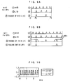
FIGS. 1A and 1B are diagrams showing the four types of
basic unit filters F0 to F3; FIG. 1A shows the circuit structure
and FIG. 1B shows numeric strings of filter coefficients. As
shown in FIG. 1A, in the basic unit filters F0 to F3, five
cascade connected D-type flip flops 1-1 to 1-5 delay an input
signal sequentially by 1 clock CK at a time. Then, the signals
extracted from the input/output taps of the respective D-type
flip flops 1-1 to 1-5 are multiplied by integer values h1 to
h6 resulting from multiplying the filter coefficients 16-fold
using six coefficient multipliers 2-1 to 2-6 respectively and
all the multiplication results are added up using five adders
3-1 to 3-5. Furthermore, by multiplying the addition output
1/16-fold using a multiplier 4 provided at the output stage
of the adder 3-5 at the final stage, the signal is output with
the amplitude returned to the original state.
-
All of the four types of basic unit filters F0 to F3 have
the circuit structure shown in FIG. 1A and only the filter
coefficients (multiplier values h1 to h6 of coefficient
multipliers 2-1 to 2-6) are different as shown in FIG. 1B. As
is evident from FIG. 1B, the filter coefficients of the basic
unit filters F0 to F3 consist of extremely simple numeric
strings using only "1" or "8" as absolute value and those strings
are differentiated by adding positive or negative signs.
However, in all the coefficients of the basic unit filters
F0 to F3, the absolute values of multiplier values h3, h4
corresponding to the taps close to the center are "8", while
the absolute values of multiplier values h1, h2, h5, h6
corresponding to the taps on both sides are "1".
-
Unit filters L1n, L2n, H1n, H2n are generated using these
basic unit filters F0 to F3. The suffix "n" to each numeral
indicating the unit filter denotes the number of clocks of
a delay to be inserted between taps, that is, the number of
"0"s to be inserted between filter coefficients (which will
be explained in detail later).
-
FIGS. 2A and 2B are diagrams showing a low-pass unit filter
L10; FIG. 2A shows a method of generating the low-pass unit
filter L10 and FIG. 2B shows the circuit structure. As shown
in FIG. 2A, the low-pass unit filter L10 is generated by carrying
out a moving average calculation on the filter coefficients
of the basic unit filter F0 one time.
-
According to the circuit structure, as shown in FIG. 2B,
a D-type flip flop 12 connected after a basic unit filter (F0)
11 delays the output signal of the basic unit filter 11 by
1 clock CK, an adder 13 adds up the signals before and after
being delayed by the D-type flip flop 12 and a multiplier 14
multiplies the addition output 1/2-fold so as to output the
signal with the amplitude returned to the original value.
-
FIGS. 3A and 3B are diagrams showing a low-pass unit filter
L11; FIG. 3A shows a method of generating the low-pass unit
filter L11 and FIG. 3B shows the circuit structure. The filter
coefficients of the low-pass unit filter L11 are generated
by inserting one "0" between the respective filter coefficients
of the aforementioned low-pass unit filter L10. That is, as
shown in FIG. 3A, the filter coefficients of the low-pass unit
filter L11 are generated by carrying out a moving average
calculation on the filter coefficients of the basic unit filter
F01 one time.
-
According to the circuit structure of the low-pass unit
filter L11, as shown in FIG. 3B, two D- type flip flops 22-1,
22-2 cascade connected after a basic unit filter (F01) 21 delay
the output signal of the basic unit filter 21 sequentially
by 1 clock CK at a time. Then, an adder 23 adds up the signals
before and after being delayed by the D- type flip flops 22-1,
22-2 and a multiplier 24 multiplies the addition output 1/2-fold
so as to output the signal with the amplitude returned to the
original value.
-
Likewise, the filter coefficients of a low-pass unit
filter L1n (n = 2, 3, ... ) are generated by inserting n "0"s
between the respective filter coefficients of the low-pass
unit filter L10.
-
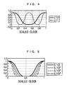
FIG. 4 is a diagram showing the frequency-gain
characteristics of the low-pass unit filters L10, L11. Here,
gain and frequency are scaled by "1". As is evident from this
FIG. 4, when the number of "0"s to be inserted between filter
coefficients is n, the frequency axis (period with respect
to the frequency direction) of the frequency-gain
characteristic becomes 1/n.
-
Next, the cascade connection of unit filters will be
explained. By cascade connecting low-pass unit filters,
coefficients of the respective unit filters are mutually
multiplied and added and new filter coefficients are created.
Hereafter, suppose when, for example, the number of cascade
connections of the low-pass unit filter L10 is m, this will
be described as (L10)m.
-
FIG. 5 is a diagram showing the frequency-gain
characteristics of low-pass unit filters L10, (L10)2, (L10)4,
(L10)8. In this FIG. 5, gain and frequency are also scaled
by "1". When there is only one low-pass unit filter L10, the
clock at a position at which the amplitude becomes 0.5 is 0.25.
In contrast to this, as the number of cascade connections m
increases, the band pass width of the filter becomes narrower.
For example, when m = 8, the clock at a position at which the
amplitude becomes 0.5 is 0.125.
-
FIGS. 6A and 6B are diagrams showing a high-pass unit
filter H10; FIG. 6A shows a method of generating the high-pass
unit filter H10 and FIG. 6B shows the circuit structure. As
shown in FIG. 6A, the filter coefficients of the high-pass
unit filter H10 are generated by carrying out a moving average
calculation one time using the filter coefficients of the basic
unit filters F2, F3.
-
According to the circuit structure, as shown in FIG. 6B,
an input signal passes through two basic unit filters (F2)
41, (F3) 42 and the output signal of the one basic unit filter
42 is delayed by 1 clock CK by a D-type flip flop 43 connected
after the basic unit filter 42. An adder 44 adds up the output
signal of the basic unit filter 41 and the output signal of
the basic unit filter 42 which has been delayed by 1 clock
by the D-type flip flop 43 and a multiplier 45 multiplies the
addition output 1/2-fold so as to output the signal with the
amplitude returned to the original value.
-
As in the case of the above described low-pass unit filter
L1n, the filter coefficients of a high-pass unit filter H1n
(n ≥ 1) are generated by inserting n "0"s between the respective
filter coefficients of the high-pass unit filter H10.
Furthermore, by cascade connecting m high-pass unit filters
H1n, it is possible to create new filter coefficients. In
the frequency-gain characteristic of a high-pass unit filter
(H1n)m, the band pass width becomes narrower as the number
of cascade connections m increases and the gain in the
high-frequency region drops extremely deeply and straightly.
-
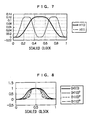
FIG. 7 is a diagram showing the frequency-gain
characteristics of the high-pass unit filters H10, H11. In
this FIG. 7, gain and frequency are also scaled by "1". As
is evident from FIG. 7, in the case of a high-pass unit filter
H1n, inserting n "0"s between filter coefficients causes the
frequency axis (period with respect to the frequency direction)
of the frequency-gain characteristic to become 1/n.
-
Furthermore, FIG. 8 is a diagram showing the
frequency-gain characteristics of the high-pass unit filters
H10, (H10)2, (H10)4, (H10)8. In this FIG. 8, gain and frequency
are also scaled by "1". When there is only one high-pass unit
filter H10, the clock at a position at which the amplitude
becomes 0.5 is 0.25. In contrast to this, as the number of
cascade connections m increases, the band pass width of the
filter becomes narrower. For example, when m = 8, the clock
at a position at which the amplitude becomes 0.5 is 0.375.
-
This is the basic content of the previous application.
The filter designing method according to this embodiment will
be explained below. Here, an example where a band pass filter
having a desired frequency band as a pass band is designed
by combining the aforementioned low-pass unit filter L1n and
high-pass unit filter H1n will be explained.
-
When any one of a center frequency Fc of a band pass filter
and signal sampling frequency Fs can be determined freely,
it is possible to simplify the filter structure by optimizing
the condition for pulling out frequencies. Now, suppose the
relationship between the center frequency Fc of the band pass
filter and signal sampling frequency Fs is:
Fs = Fc * (4 + 2k) (k = 0, 1, 2, ...)
-
In this case, when Fc = 450 KHz, Fs = 1.8 MHz, 2.7 MHz,
3.6 MHz, .... In the case of such a setting, it is possible
to design a band pass filter by only cascade connecting a
high-pass unit filter H1(5 + 3k) and a low-pass unit filter
L1(3 + 2k). Both the high-pass unit filter H1(5 + 3k) and
low-pass unit filter L1(3 + 2k) have a pass band whose center
frequency Fc becomes 450 KHz.
-
For example, when k = 0 (Fs = 4Fc), it is possible to
design a band pass filter by cascade connecting a high-pass
unit filter H15 and a low-pass unit filter L13. Furthermore,
when k = 1(Fs = 6Fc), it is possible to design a band pass
filter by cascade connecting a high-pass unit filter H18 and
a low-pass unit filter L15.
-
FIGS. 9A and 9B are diagrams schematically showing a
method of designing the aforementioned band pass filter; FIG.
9A shows a case where k = 0 and FIG. 9B shows a case where
k = 1. For example, in FIG. 9A, when the high-pass unit filter
H15 and low-pass unit filter L13 are cascade connected, only
the superimposed portions between pass bands (1), (2) can be
extracted as a pass band (3).
-
Likewise in FIG. 9B, when the high-pass unit filter H18
and low-pass unit filter L15 are cascade connected, only the
superimposed portions between pass bands (1), (2) can be
extracted as a pass band (3), too. When k > 0, pass bands
other than the center frequency Fc of the band pass filter
to be obtained are generated, and therefore these pass bands
are pulled out by a low-pass filter (LPF1) (4).
-
The band width of the band pass filter can be adjusted
by the number of cascade connected stages (number of m) of
high-pass unit filter (H1n)m or low-pass unit filter (L1n)m.
In the example shown in FIG. 9B, both the high-pass unit filter
H18 and low-pass unit filter L15 have m = 1. FIG. 10 and FIG.
11 show the frequency characteristics when m = 8.
-
FIG. 10 shows the frequency characteristics of the
high-pass unit filter (H18)8 and low-pass unit filter (L15)8
superimposed on each other. By cascade connecting these filters,
it is possible to extract only the superimposed portions.
Furthermore, FIG. 11 shows pulling out of pass bands by the
LPF1 or LPF2. By applying the LPF1 or LPF2 to the three band
passes extracted as shown in FIG. 10, it is possible to extract
only the pass bands at both ends.
-
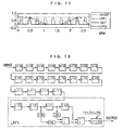
Next, an actual circuit example will be shown. Suppose
a target standard has a center frequency Fc = 450 KHz, -3 dB
band width = 100 KHz, -80 dB band width = 200 KHz. FIG. 12
is a diagram showing a circuit example of a band pass filter
which realizes this target standard.
-
The amount of attenuation of a band pass depends on the
number of cascade connected filters. In the circuit shown
in FIG. 12, four low-pass unit filters L111 are further cascade
connected after eight high-pass unit filters H18 and eight
low-pass unit filters L15 to secure an amount of attenuation
of 80 dB or more. Low-pass unit filters (L10)2, L11, L12,
D-type flip flops D9, D6 and several multipliers and adders
that follow these unit filters constitute an LPF1. The D9,
D6 mean delays of 9 clocks, 6 clocks, respectively.
-
As is evident from this FIG. 12, according to the filter
designing method of this embodiment, it is possible to obtain
a band pass filter having a desired characteristic in an
extremely simple structure consisting of a repetition of
substantially the same unit filter. Furthermore, the
internal structure of each unit filter is as described above,
the total number of taps required is 144, which is very few
in number. Furthermore, filter coefficients necessary for
each tap output are of only four types of -1/16, 1/16, -8/16,
8/16, and since -8/16 = -1/2, 8/16 = 1/2 in particular, it
is possible to simplify the calculation circuit considerably.
-
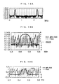
FIGS. 13A to 13C are diagrams showing the frequency-gain
characteristic of the band pass filter constructed as shown
in FIG. 12. FIG. 13A shows the overall frequency
characteristic and shows the gain on a logarithmic scale. FIGS.
13B and 13C show enlarged views of a portion of the pass band;
FIG. 13B shows the gain on a logarithmic scale and FIG. 13C
shows the gain on a linear scale.
-
As is evident from FIG. 13A, the band pass filter
constructed as shown in FIG. 12 can realize an amount of
attenuation of 80 dB or more. However, the band width at -3
dB is approximately 63 KHz and the band width at -80 dB is
approximately 145 KHz, which do not satisfy required
specifications. In the circuit in FIG. 12, k = 1 (Fs = 6Fc),
but when a greater band width is required, it is possible to
set k ≥ 2 and increase the sampling frequency Fs.
-
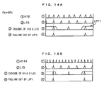
Next, adjusting means for narrowing a band width will
be explained. As described above using FIG. 5 and FIG. 8,
the number of stages of cascade connected filters can be
increased to narrow the band width, which however has a limit.
Here, a method capable of narrowing the band width more
efficiently will be explained. FIG. 14 schematically shows
the method.
-
FIG. 14A is the same as FIG. 9B. To obtain a narrower
band width than this, a high-pass unit filter H114 is used
instead of the high-pass unit filter H18 as shown in FIG. 14B.
Just like the high-pass unit filter H18, the high-pass unit
filter H114 has a pass band with a center frequency Fc of 450
KHz. Besides, the band width of the high-pass unit filter H114
is 9/15 = 3/5 of that of the high-pass unit filter H18.
-
Therefore, using this high-pass unit filter H114 allows
the band width to be narrowed efficiently without increasing
the number of stages of cascade connected filters.
Furthermore, since the high-pass unit filter H114 has simply
increased the number of "0"s to be inserted between the
respective filter coefficients, the number of taps to be
actually extracted as coefficients does not increase at all
and the circuit scale does not expand either. Here, an example
of using the high-pass unit filter H114 has been explained,
but any unit filter having a pass band at the same center
frequency Fc = 450 KHz can be used likewise.
-
Next, adjusting means for widening the band width will
be explained. FIG. 15 is a frequency-gain characteristic
diagram to show a method of adjusting a band width including
a gradient. In this FIG. 15, the gain is also scaled by "1".
Here, suppose the frequency characteristic of the unit filter
before adjustment is expressed by YF. As described above,
when two unit filters YF shown in (1) are cascade connected,
the gradient becomes steeper and the band with becomes narrower
(the clock position at -6 dB is shifted toward the lower
frequency side) ((2)).
-
Then, the frequency-gain characteristic of the unit
filter YF2 shown in (2) is inverted using the central value
(= 0.5) of the gain as the axis ((3)). This can be obtained
by subtracting the filter coefficients of the unit filter YF2
from a unit pulse having a reference gain value of "1"
(corresponding to a filter coefficient having a central value
being "1" and all others being "0") (1-YF2) after adjusting
the delay. Here, this will be called an "inverted unit filter."
-
Furthermore, two inverted unit filters shown in (3) are
cascade connected. The gradient of the frequency-gain
characteristic obtained in this way becomes further steeper
and the band width also becomes narrower (the clock position
at -6 dB moves toward a high frequency side) ((4)). Here,
the number of cascade connected inverted unit filters is
assumed to be 2 as in the case of (2), but increasing this
number can increase the amount of movement toward the high
frequency side compared to the amount of movement toward the
low frequency side which has been described above.
-
Finally, the frequency-gain characteristic shown in (4)
is inverted using the central value of the gain (= 0.5) as
the axis ((5)). This can be calculated by subtracting the
filter coefficient in (4) from the unit pulse having a reference
gain value of "1" (1-(1-YF2)2) after adjusting the delay. When
the frequency characteristic of the original data (1) is
compared with the frequency characteristic of the adjusted
data (5), the gradient of the frequency characteristic of the
adjusted data (5) becomes steeper than that of the original
data (1) and the band width becomes wider.
-
The expression of the adjusted data (5) is developed as
follows:
-
This Expression 1 is the expression obtained when two
unit filters in (1) and two inverted unit filters in (3) are
cascade connected, but the number of cascade connected stages
is not limited to this. However, to widen the band width,
it is more desirable to make more the number of cascade connected
stages in (3) than the number of cascade connected stages in
(1).
-
In this case, the above described Expression 1 can be
generalized as Expression 2 shown below:
a * YFi - b * YFj
where a, b denote coefficients (a > b), i < j, and * denotes
a cascade connection. FIG. 16 shows an example of the result
of adjusting this band width using the high-pass unit filter
H18 as the original data before adjustment. Here, the adjusted
filter is assumed to be:
2 * (H18)5 - (H18)9
-
Because of this adjustment, the band width at -3 dB is
approximately 100 KHz and the band width at -50 dB is
approximately 200 KHz.
-
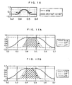
Next, the means for fine-adjusting the frequency of the
band width will be explained. FIGS. 17A and 17B show
frequency-gain characteristic diagrams for illustrating a
method of fine-adjusting the frequency. In this FIG. 17, the
gain is also scaled by "1".
-
As shown in FIG. 17, a high-pass filter (HPF) and a low-pass
filter (LPF) are designed so that pass bands overlap with each
other in a relatively wide pass band of the high-pass unit
filter H18. By cascade connecting these filters H18, HPF,
LPF, it is possible to obtain a band pass filter in which a
superimposed portion of the respective pass bands (diagonally
shaded area) becomes a pass band.
-
At this time, by carrying out an operation of narrowing
the pass band as shown in FIG. 5 and FIG. 8 or FIG. 14 or an
operation of widening the pass band as shown in FIG. 15 and
FIG. 16 on any one or both of the high-pass filter HPF and
low-pass filter LPF, it is possible to arbitrarily fine-adjust
the band width of the band pass filter.
-
FIG. 17A shows an example of shifting only one side of
the band pass filter toward the high frequency side by carrying
out an operation of widening the pass band on the low-pass
filter LPF. On the other hand, FIG. 17B shows an example of
shifting both sides of the band pass filter toward the low
frequency side without changing the band width by carrying
out an operation of widening the pass band on the high-pass
filter HPF and at the same time carrying out an operation of
narrowing the pass band on the low-pass filter LPF.
-
The apparatus for realizing the digital filter designing
method according to this embodiment described above can be
implemented by any one of a hardware structure, DSP or software.
For example, when the apparatus is implemented by software,
the filter designing apparatus of this embodiment is actually
constructed of a CPU or MPU, RAM, ROM, etc., of a computer
and can be implemented by operating a program stored in the
RAM or ROM or hard disk, etc.
-
Therefore, it is possible to realize the apparatus by
recording a program which causes the computer to operate so
as to execute the functions of this embodiment in a recording
medium such as a CD-ROM and causing the computer to read the
program. In addition to the CD-ROM, the recording medium for
recording the aforementioned program can be a flexible disk,
hard disk, magnetic tape, optical disk, magneto-optical disk,
DVD, non-volatile memory card, etc. The apparatus can also
be implemented by downloading the above described program to
the computer via a network such as the Internet.
-
That is, it is possible to store filter coefficients about
various types of unit filters L1n, H1n, etc., as information
in a memory such as RAM or ROM, cause the CPU, when the user
instructs an arbitrary combination about the unit filters L1n,
H1n, etc., to calculate filter coefficients corresponding to
the instructed combination using the information on filter
coefficients stored in the memory.
-
For example, it is also possible to iconize various types
of unit filters L1n, H1n (storing filter coefficients as
information corresponding to each icon) so that the user can
arbitrarily combine and arband these icons on the display
screen and cause the CPU to automatically calculate and acquire
the filter coefficient corresponding to the string of filter
coefficients. Furthermore, if the calculated filter
coefficient is automatically FFT-transformed and the result
is displayed as a frequency-gain characteristic diagram, it
is possible to confirm the characteristic of the designed
filter and design filters more easily.
-
In not only the case where the functions of the above
described embodiment are realized by the computer executing
the supplied program but also a case where the functions of
the above described embodiments are realized by the program
in cooperation with the OS (operating system) or other
application software, etc., operating on the computer or a
case where the functions of the above described embodiment
are realized by all or part of the processing of executing
the supplied program on a function expansion board or function
expansion unit of the computer, such a program is included
in the embodiment of the present invention.
-
As detailed above, this embodiment uses one or more unit
filters based on basic unit filters having a predetermined
basic numeric string as filter coefficients, cascade connects
these unit filters to design an FIR filter having a desired
frequency characteristic. Thus, it is possible to generate
complicated filter coefficients of band pass filters by
substantially only combining unit filters. Therefore, the
filter designing method is simple and easily comprehensible
so that even non-expert technicians can design filters
extremely easily.
-
Furthermore, since the filter circuit designed by
applying this embodiment requires a very small number of taps
and requires only four types of filter coefficients of -1/16,
1/16, -8/16, 8/16 for each tap output, it is possible to make
the structure of the filter circuit extremely simple.
Therefore, it is possible to drastically reduce the number
of circuit elements (especially of multipliers), reduce the
scale of the filter circuit and reduce both power consumption
and calculation load, etc.
-
Furthermore, since the filter circuit designed by
applying this embodiment has an extremely simple structure
consisting of a repetition of substantially the same pattern,
it is possible to reduce man-hours for integration and
facilitate the integration into an IC. Furthermore, in the
aspect of the characteristic, it is possible to make quite
a large improvement in a cutoff characteristic and obtain a
linear and excellent filter characteristic in the phase
characteristic, too.
-
Furthermore, when any one of the center frequency Fc of
the band pass filter or signal sampling frequency Fs can be
freely determined, this embodiment allows a band pass filter
to be designed by only cascade connecting the high-pass unit
filter H1(5 + 3k) and low-pass unit filter L1(3 + 2k). This
eliminates the necessity for extracting necessary frequency
bands by canceling out characteristic values which combine
several types of unit filters, allows a band pass filter to
be designed extremely easily and can make the filter structure
simpler.
-
In this case, by designing a band pass filter with unit
filters having the same filter center frequency Fc and more
"0"s inserted between filter coefficients (large k value)
cascade connected, it is possible to efficiently narrow the
band width without increasing the number of stages of cascade
connected filters or the number of taps. That is, it is
possible to simply narrow the band width without increasing
the circuit scale of the filter.
-
Furthermore, this embodiment also allows the band width
to be arbitrarily widened by only cascade connecting the unit
filters in such a way as to satisfy the relationship:
a * (H1n)i - b * (H1n)j
or
a * (L1n)i - b * (L1n)j
- (a, b, i, j: coefficients; a > b, i < j)
-
-
Furthermore, using the operation of widening the band
width and operation of narrowing the band width makes it
possible to simply fine-adjust the band width. This makes
it possible to realize a desired frequency characteristic more
accurately and design the FIR digital filter having such a
frequency characteristic more easily.
-
The above described embodiment has shown L0 to L3 as
examples of basic unit filters, but the present invention is
not limited to this. That is, it is also possible to use numeric
values having absolute values of "1" and "8" to set a numeric
string different from that in FIG. 1B as filter coefficients
of the basic unit filters. Furthermore, the above described
embodiment has shown two types; L1n, H1n as examples of the
unit filter, but the present invention is not limited to this.
-
Furthermore, the above described embodiment has used a
numeric string with absolute values having a ratio of 1, 1,
8, 8, 1, 1 as the filter coefficients of the basic unit filters ,
but it is also possible to use a numeric string with absolute
values having a ratio of 1, 0, 9, 16, 9, 0, 1 obtained by moving
averaging this numeric string once.
-
Furthermore, the above described embodiment has mainly
explained an example of designing a band pass filter, but it
is also possible to design a high-pass filter, low-pass filter,
band elimination filter, etc., using similar techniques. The
techniques for designing these filters will be explained below
in a simple manner.
<When a band pass filter is created>
-
- (1) High-pass unit filters H11 are cascade connected
(limited to Fs = 4 * Fc).
- (2) A high-pass filter HPF and low-pass filter LPF are
used.
- (3) Ahigh-pass filter and low-pass filter with respective
pass bands overlapping with each other are created. (Mutually
overlapping band pass filters are also acceptable.)
-
<When a high-pass filter is created>
-
- (1) High-pass unit filters H10 are cascade connected.
- (2) (H10)m1 * (H11)m2 is created.
-
<When a low-pass filter is created>
-
- (1) Low-pass unit filters L10 are cascade connected.
- (2) (L10)m1 * (L11)m2 is created.
-
<When a band elimination filter is created>
-
- (1) The frequency-gain characteristic of a band pass
filter is inverted using the central value of the gain as the
axis. More specifically, a maximum value of coefficients of
the band pass filter is subtracted from a reference gain value
of "1" and the polarities of other coefficients are inverted.
This is obtained by subtracting the filter coefficient of the
band pass filter from a unit pulse having a reference gain
value of "1" after adjusting the delay.
-
-
Furthermore, it is also possible to design a digital filter
by dividing the filter string generated using the above
described designing method into one or more blocks and cascade
connecting one or more filters which are final generation
coefficients for each block.
-
In addition, all the above described embodiments have
only shown specific examples in implementing the present
invention and this should not cause the technological scope
of the present invention to be interpreted in a limited way.
That is, the present invention can be implemented in various
forms without departing from the spirit ormain characteristics
thereof.
[Industrial Applicability]
-
The present invention is useful for realizing a desired
frequency characteristic at a higher degree of accuracy and
enabling an FIR digital filter having such a frequency
characteristic to be designed more easily.