EP1533887A1 - Pwm inverter control method - Google Patents
Pwm inverter control method Download PDFInfo
- Publication number
- EP1533887A1 EP1533887A1 EP03723402A EP03723402A EP1533887A1 EP 1533887 A1 EP1533887 A1 EP 1533887A1 EP 03723402 A EP03723402 A EP 03723402A EP 03723402 A EP03723402 A EP 03723402A EP 1533887 A1 EP1533887 A1 EP 1533887A1
- Authority
- EP
- European Patent Office
- Prior art keywords
- switching
- switching operations
- pwm
- operations
- control method
- Prior art date
- Legal status (The legal status is an assumption and is not a legal conclusion. Google has not performed a legal analysis and makes no representation as to the accuracy of the status listed.)
- Granted
Links
Images




Classifications
-
- H—ELECTRICITY
- H02—GENERATION; CONVERSION OR DISTRIBUTION OF ELECTRIC POWER
- H02M—APPARATUS FOR CONVERSION BETWEEN AC AND AC, BETWEEN AC AND DC, OR BETWEEN DC AND DC, AND FOR USE WITH MAINS OR SIMILAR POWER SUPPLY SYSTEMS; CONVERSION OF DC OR AC INPUT POWER INTO SURGE OUTPUT POWER; CONTROL OR REGULATION THEREOF
- H02M7/00—Conversion of AC power input into DC power output; Conversion of DC power input into AC power output
- H02M7/42—Conversion of DC power input into AC power output without possibility of reversal
- H02M7/44—Conversion of DC power input into AC power output without possibility of reversal by static converters
- H02M7/48—Conversion of DC power input into AC power output without possibility of reversal by static converters using discharge tubes with control electrode or semiconductor devices with control electrode
- H02M7/483—Converters with outputs that each can have more than two voltages levels
- H02M7/487—Neutral point clamped inverters
-
- H—ELECTRICITY
- H02—GENERATION; CONVERSION OR DISTRIBUTION OF ELECTRIC POWER
- H02M—APPARATUS FOR CONVERSION BETWEEN AC AND AC, BETWEEN AC AND DC, OR BETWEEN DC AND DC, AND FOR USE WITH MAINS OR SIMILAR POWER SUPPLY SYSTEMS; CONVERSION OF DC OR AC INPUT POWER INTO SURGE OUTPUT POWER; CONTROL OR REGULATION THEREOF
- H02M7/00—Conversion of AC power input into DC power output; Conversion of DC power input into AC power output
- H02M7/42—Conversion of DC power input into AC power output without possibility of reversal
- H02M7/44—Conversion of DC power input into AC power output without possibility of reversal by static converters
- H02M7/48—Conversion of DC power input into AC power output without possibility of reversal by static converters using discharge tubes with control electrode or semiconductor devices with control electrode
- H02M7/505—Conversion of DC power input into AC power output without possibility of reversal by static converters using discharge tubes with control electrode or semiconductor devices with control electrode using devices of a thyratron or thyristor type requiring extinguishing means
- H02M7/515—Conversion of DC power input into AC power output without possibility of reversal by static converters using discharge tubes with control electrode or semiconductor devices with control electrode using devices of a thyratron or thyristor type requiring extinguishing means using semiconductor devices only
- H02M7/525—Conversion of DC power input into AC power output without possibility of reversal by static converters using discharge tubes with control electrode or semiconductor devices with control electrode using devices of a thyratron or thyristor type requiring extinguishing means using semiconductor devices only with automatic control of output waveform or frequency
- H02M7/527—Conversion of DC power input into AC power output without possibility of reversal by static converters using discharge tubes with control electrode or semiconductor devices with control electrode using devices of a thyratron or thyristor type requiring extinguishing means using semiconductor devices only with automatic control of output waveform or frequency by pulse width modulation
-
- H—ELECTRICITY
- H02—GENERATION; CONVERSION OR DISTRIBUTION OF ELECTRIC POWER
- H02M—APPARATUS FOR CONVERSION BETWEEN AC AND AC, BETWEEN AC AND DC, OR BETWEEN DC AND DC, AND FOR USE WITH MAINS OR SIMILAR POWER SUPPLY SYSTEMS; CONVERSION OF DC OR AC INPUT POWER INTO SURGE OUTPUT POWER; CONTROL OR REGULATION THEREOF
- H02M1/00—Details of apparatus for conversion
- H02M1/44—Circuits or arrangements for compensating for electromagnetic interference in converters or inverters
-
- H—ELECTRICITY
- H02—GENERATION; CONVERSION OR DISTRIBUTION OF ELECTRIC POWER
- H02M—APPARATUS FOR CONVERSION BETWEEN AC AND AC, BETWEEN AC AND DC, OR BETWEEN DC AND DC, AND FOR USE WITH MAINS OR SIMILAR POWER SUPPLY SYSTEMS; CONVERSION OF DC OR AC INPUT POWER INTO SURGE OUTPUT POWER; CONTROL OR REGULATION THEREOF
- H02M7/00—Conversion of AC power input into DC power output; Conversion of DC power input into AC power output
- H02M7/42—Conversion of DC power input into AC power output without possibility of reversal
- H02M7/44—Conversion of DC power input into AC power output without possibility of reversal by static converters
- H02M7/48—Conversion of DC power input into AC power output without possibility of reversal by static converters using discharge tubes with control electrode or semiconductor devices with control electrode
-
- H—ELECTRICITY
- H02—GENERATION; CONVERSION OR DISTRIBUTION OF ELECTRIC POWER
- H02M—APPARATUS FOR CONVERSION BETWEEN AC AND AC, BETWEEN AC AND DC, OR BETWEEN DC AND DC, AND FOR USE WITH MAINS OR SIMILAR POWER SUPPLY SYSTEMS; CONVERSION OF DC OR AC INPUT POWER INTO SURGE OUTPUT POWER; CONTROL OR REGULATION THEREOF
- H02M7/00—Conversion of AC power input into DC power output; Conversion of DC power input into AC power output
- H02M7/42—Conversion of DC power input into AC power output without possibility of reversal
- H02M7/44—Conversion of DC power input into AC power output without possibility of reversal by static converters
- H02M7/48—Conversion of DC power input into AC power output without possibility of reversal by static converters using discharge tubes with control electrode or semiconductor devices with control electrode
- H02M7/53—Conversion of DC power input into AC power output without possibility of reversal by static converters using discharge tubes with control electrode or semiconductor devices with control electrode using devices of a triode or transistor type requiring continuous application of a control signal
- H02M7/537—Conversion of DC power input into AC power output without possibility of reversal by static converters using discharge tubes with control electrode or semiconductor devices with control electrode using devices of a triode or transistor type requiring continuous application of a control signal using semiconductor devices only, e.g. single switched pulse inverters
- H02M7/5387—Conversion of DC power input into AC power output without possibility of reversal by static converters using discharge tubes with control electrode or semiconductor devices with control electrode using devices of a triode or transistor type requiring continuous application of a control signal using semiconductor devices only, e.g. single switched pulse inverters in a bridge configuration
- H02M7/53871—Conversion of DC power input into AC power output without possibility of reversal by static converters using discharge tubes with control electrode or semiconductor devices with control electrode using devices of a triode or transistor type requiring continuous application of a control signal using semiconductor devices only, e.g. single switched pulse inverters in a bridge configuration with automatic control of output voltage or current
- H02M7/53875—Conversion of DC power input into AC power output without possibility of reversal by static converters using discharge tubes with control electrode or semiconductor devices with control electrode using devices of a triode or transistor type requiring continuous application of a control signal using semiconductor devices only, e.g. single switched pulse inverters in a bridge configuration with automatic control of output voltage or current with analogue control of three-phase output
-
- H—ELECTRICITY
- H02—GENERATION; CONVERSION OR DISTRIBUTION OF ELECTRIC POWER
- H02M—APPARATUS FOR CONVERSION BETWEEN AC AND AC, BETWEEN AC AND DC, OR BETWEEN DC AND DC, AND FOR USE WITH MAINS OR SIMILAR POWER SUPPLY SYSTEMS; CONVERSION OF DC OR AC INPUT POWER INTO SURGE OUTPUT POWER; CONTROL OR REGULATION THEREOF
- H02M7/00—Conversion of AC power input into DC power output; Conversion of DC power input into AC power output
- H02M7/42—Conversion of DC power input into AC power output without possibility of reversal
- H02M7/44—Conversion of DC power input into AC power output without possibility of reversal by static converters
- H02M7/48—Conversion of DC power input into AC power output without possibility of reversal by static converters using discharge tubes with control electrode or semiconductor devices with control electrode
- H02M7/53—Conversion of DC power input into AC power output without possibility of reversal by static converters using discharge tubes with control electrode or semiconductor devices with control electrode using devices of a triode or transistor type requiring continuous application of a control signal
- H02M7/537—Conversion of DC power input into AC power output without possibility of reversal by static converters using discharge tubes with control electrode or semiconductor devices with control electrode using devices of a triode or transistor type requiring continuous application of a control signal using semiconductor devices only, e.g. single switched pulse inverters
- H02M7/5387—Conversion of DC power input into AC power output without possibility of reversal by static converters using discharge tubes with control electrode or semiconductor devices with control electrode using devices of a triode or transistor type requiring continuous application of a control signal using semiconductor devices only, e.g. single switched pulse inverters in a bridge configuration
- H02M7/53871—Conversion of DC power input into AC power output without possibility of reversal by static converters using discharge tubes with control electrode or semiconductor devices with control electrode using devices of a triode or transistor type requiring continuous application of a control signal using semiconductor devices only, e.g. single switched pulse inverters in a bridge configuration with automatic control of output voltage or current
- H02M7/53875—Conversion of DC power input into AC power output without possibility of reversal by static converters using discharge tubes with control electrode or semiconductor devices with control electrode using devices of a triode or transistor type requiring continuous application of a control signal using semiconductor devices only, e.g. single switched pulse inverters in a bridge configuration with automatic control of output voltage or current with analogue control of three-phase output
- H02M7/53876—Conversion of DC power input into AC power output without possibility of reversal by static converters using discharge tubes with control electrode or semiconductor devices with control electrode using devices of a triode or transistor type requiring continuous application of a control signal using semiconductor devices only, e.g. single switched pulse inverters in a bridge configuration with automatic control of output voltage or current with analogue control of three-phase output based on synthesising a desired voltage vector via the selection of appropriate fundamental voltage vectors, and corresponding dwelling times
Definitions
- the present invention relates to a reduction in the noise of a PWM inverter for carrying out the variable speed driving operation and system interconnection of a motor.
- Fig. 13 is a diagram showing the structure of a conventional PWM inverter.
- 1 denotes a controller
- 2 denotes a noise reducing PWM generating circuit
- 4 denotes a current detecting circuit
- 5 denotes a DC power supply
- 11 denotes a smoothing capacitor
- 101 to 106 denote a switching unit
- 201 to 206 denote a free wheel diode.
- a command and a detection value of an output current from the current detecting circuit 4 are input to the controller 1.
- the controller 1 creates a PWM switching pattern specialized to reduce a noise by the noise reducing PWM generating circuit 2 in response to their inputs and outputs a command for turning ON/OFF a switching unit.
- a PWM pulse having a 3-phase and 2-level which is output from the circuit shown in Fig. 13 is illustrated in a spatial vector diagram of Fig. 2, and a general PWM pulse pattern is shown in Fig. 3.
- Each of symbols a, b, Op and On vectors on the spatial vector diagram of Fig. 2 corresponds to the switching pattern of each phase shown in Fig. 3, and H indicates a state in which an upper switching unit is ON and L indicates a state in which a lower switching unit is ON.
- a PWM inverter usually outputs the pattern shown in Fig. 3, and furthermore, outputs a noise reducing pattern shown in Fig. 4 which is obtained by recombining a pulse pattern by the noise reducing PWM generating circuit 2.
- the noise reducing pattern is equal to the ordinary pattern of Fig. 3 on a time average, and the pulse pattern shown in Fig. 4 in which a pulse is divided, converged and distributed is generated to disperse a noise, whereby a noise reduction can be thus attained.
- a first aspect of the invention is directed to a PWM inverter control method of a 2-level PWM control type which has a function of freely changing switching of switching units connected in series every set in a structure in which two switches including a switching unit and a rectifying unit connected in antiparallel are serially connected in plural sets, wherein the switching of the switching units connected in series is limited by setting the number of switching operations and a timing to output an optional voltage in order not to converge a frequency component of a noise caused by the switching and setting a lower limit to the number of switching operations in order to prevent the number of switching operations from being excessively decreased in that case when an operation frequency of an inverter is low, and increasing the number of switching operations and a set value of the timing in a constant ratio to the operation frequency and setting an upper limit to the number of switching operations in such a manner that the number of switching operations does not exceed a certain set value when the operation frequency of the inverter is increased.
- the PWM inverter control method in a 2-level PWM inverter control method capable of freely setting the switching of each phase, the peak of a noise is dispersed and the number of switching operations is provided with an upper limit value and a lower limit value and is thus limited. Consequently, it is also possible to reduce an unpleasant noise and to suppress a switching loss.
- a second aspect of the invention is directed to a PWM inverter control method of a multilevel PWM control type which has a function of freely changing switching of switching units connected in series every set and outputs a PWM pulse having at least three output levels in a structure in which at least four even-numbered switches including a switching unit and a rectifying unit connected in antiparallel are serially connected in plural sets, wherein the switching of the switching units connected in series is limited by setting the number of switching operations and a timing to output an optional voltage in order not to converge a frequency component of a noise caused by the switching and setting a lower limit to the number of switching operations in order to prevent the number of switching operations from being excessively decreased in that case when an operation frequency of an inverter is low, and increasing the number of switching operations and a set value of the timing in a constant ratio to the operation frequency and setting an upper limit to the number of switching operations in such a manner that the number of switching operations does not exceed a certain set value when the operation frequency of the inverter is increased.
- the peak of a noise is dispersed and the number of switching operations is provided with an upper limit value and a lower limit value and is thus limited. Consequently, it is also possible to reduce an unpleasant noise and to suppress a switching loss.
- a third aspect of the invention is directed to the PWM inverter control method according to the first or second aspect of the invention, wherein an upper limit value of the number of switching operations is set in such a manner that a time average of a switching loss generated by the switching unit is equal to or smaller than a certain set value.
- the upper limit value of a switching number limitation is set in such a manner that the time average of the switching loss is equal to or smaller than the set value.
- a fourth aspect of the invention is directed to the PWM inverter control method according to the first or second aspect of the invention, wherein an upper limit value of the number of switching operations is set in such a manner that generation of heat of a PWM inverter is equal to or smaller than a certain set value.
- the upper limit value of the switching number limitation is set in such a manner that the generation of heat of the inverter is equal or smaller than the set value.
- a fifth aspect of the invention is directed to the PWM inverter control method according to any of the first to fourth aspects of the invention, wherein a frequency of the number of switching operations to be set is skipped in such a manner that a component of the frequency is not equal to a resonance frequency of a motor connected to an output side.
- a noise can be reduced and a switching loss can be suppressed through the limitation of the number of switching operations, and furthermore, the vibration of a control system can be controlled and the generation of a mechanical sound can also be reduced through the frequency skip of the resonance frequency band of the motor.
- Fig. 12 is a diagram showing a switching pattern subjected to a reduction in a noise and a switching number limitation in the inverter illustrated in Fig. 8.
- Fig. 13 is a diagram showing an example of the circuit of a conventional PWM inverter device.
- 1 denotes a controller
- 2 denotes a noise reducing PWM generating circuit
- 3 denotes a switching number limiting circuit
- 4 denotes a current detecting circuit
- 5 denotes a DC power supply
- 11 denotes a smoothing capacitor
- 12 and 13 denote a voltage dividing capacitor
- 101 to 118 denote a switching unit
- 201 to 218 denote a free wheel diode
- 301 to 306 denote a clamp diode.
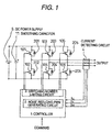
- Fig. 1 is a diagram showing an example of a circuit for a PWM inverter control method according to a first embodiment.
- Fig. 2 is a diagram showing the spatial vector of an inverter illustrated in Fig. 1.
- Fig. 3 is a diagram showing the ordinary switching pattern of the inverter illustrated in Fig. 1.
- Fig. 4 is a diagram showing a switching pattern obtained by reducing a noise in the pattern illustrated in Fig. 3.
- Fig. 5 is a diagram showing a switching pattern subjected to a reduction in a noise and a switching number limitation in the inverter illustrated in Fig. 1.
- Fig. 6 is a graph representing the switching number limitation shown in Fig. 5.
- Fig. 7 is a chart showing a skip frequency band in the graph of Fig. 6.
- Fig. 1 denotes a controller
- 2 denotes a noise reducing PWM generating circuit
- 3 denotes a switching number limiting circuit
- 4 denotes a current detecting circuit
- 5 denotes a DC power supply
- 11 denotes a smoothing capacitor
- 101 to 106 denote a switching unit
- 201 to 206 denote a free wheel diode.
- a PWM pulse pattern shown in Fig. 3 is created based on a spatial vector shown in Fig. 2 according to the command value.
- Symbols a, b, Op and On of the spatial vector in Fig. 2 correspond to the switching patterns of phases U, V and W shown in Fig. 3, and H indicates a state in which the upper switching units 101, 103 and 105 are ON, and L indicates a state in which the lower switching units 102, 104 and 106 are ON.
- the switching units "101 and 102" correspond to the U phase
- the switching units "103 and 104" correspond to the V phase
- the switching units "105 and 106" correspond to the W phase.
- the PWM pulse pattern is changed to a PWM switching pattern subjected to a reduction in a noise through the noise reducing PWM generating circuit 2.
- switching is uniformly carried out over the U, V and W phases together in Fig. 3.
- a noise output is converged on a specific frequency.
- the average value of a voltage to be output is held to be equal to that in Fig. 3, and at the same time, a pattern is divided and recombined and a frequency is thus regulated in such a manner that a specific frequency (a frequency in an unpleasant voice band) is not output. Description will be given with reference to an example of the U phase.
- the switching pattern thus subjected to the reduction in a noise is then input to the switching number limiting circuit 3 to decide whether or not a set number of switching operations is satisfied.
- the switching number limiting circuit 3 sets a limit in such a manner that the set number of switching operations is not exceeded.
- the limit may be set based on the characteristic of a switching unit (an IGBT) in the design of a PWM inverter or may be set by measurement based on the amount of generated heat under the condition of an actual use, and is not set to be a specific fixed value.
- the number of switching operations is increased simultaneously with a rise in an operation frequency, and a number limiting function is performed so that more switching is limited as shown in Fig. 6 when the number of switching operations exceeds a set value by the decision of the switching number limiting circuit 3.
- the number of divisions of a PWMpattern is decreased on a carrier cycle unit or a dispersing method is changed to carry out a regulation in order to reduce the number of switching operations in such a manner that the number of switching operations on a time average is maintained to be constant in the noise reducing PWM generating circuit 2.
- Fig. 5 shows a noise reducing pattern subjected to the switching number limitation, in which a period T1 is the same as that in the pulse pattern shown in Fig. 4 and the number of switching operations is limited to decrease pulses when a cycle is changed from T1 to T2 so that an operation frequency is increased.
- the number is 11 for the period T1 which is the same as that in Fig. 4 and the number is reduced to be seven for the period T2.
- the number of switching operations is almost equalized on a total time average and the time average of a switching loss is maintained to be equal to or smaller than a set value so that the generation of heat of the switching unit can be suppressed.
- the lower limit value of the number of switching operations is set by the switching number limiting circuit 3 (which is also set by a characteristic value) and a limit is set in such a manner that the number of switching operations is not smaller than the lower limit value.
- the number of switching operations is subjected to a skip processing as the processing of the switching number limiting circuit 3 in such a manner that the resonance frequency of a motor to be connected as a load is not coincident with the number of switching operations of a PWM pulse pattern to be output.
- Fig. 8 is a diagram showing an example of a circuit for a PWM inverter control method according to the second embodiment.
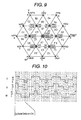
- Fig. 9 is a diagram showing the spatial vector of an inverter illustrated in Fig. 8.
- Fig. 10 is a diagram showing the ordinary switching pattern of the inverter illustrated in Fig. 8.
- Fig. 11 is a diagram showing a switching pattern obtained by reducing a noise in the pattern illustrated in Fig. 10.
- Fig. 12 is a diagram showing a switching pattern subjected to a reduction in a noise and a switching number limitation in the inverter illustrated in Fig. 8.
- Fig. 8 shows an example in which the invention is applied to a 3-phase and 3-level inverter, in which 1 denotes a controller, 2 denotes a noise reducing PWM generating circuit, 3 denotes a switching number limiting circuit, 4 denotes a current detecting circuit, 5 denotes a DC power supply, 12 and 13 denote a smoothing capacitor, 107 to 118 denote a switching unit (the switching units 107 to 110 correspond to a U phase, the switching units 111 to 114 correspond to a V phase, and the switching units 115 to 118 correspond to a W phase), 201 to 206 denote a free wheel diode, and 301 to 306 denote a clamp diode for an intermediate level output.
- 1 denotes a controller
- 2 denotes a noise reducing PWM generating circuit
- 3 denotes a switching number limiting circuit
- 4 denotes a current detecting circuit
- 5 denotes a DC power supply
- 12 and 13 denote
- a PWM pulse which can be output is represented in a spatial vector diagram as shown in Fig. 9, and a general pulse pattern using the same is shown in Fig. 10.
- a spatial vector diagram as shown in Fig. 9
- a general pulse pattern using the same is shown in Fig. 10.
- H indicates a state in which an upper switching unit is ON
- O indicates a state in which two middle switching units for outputting a neutral voltage that is capacitor divided are ON
- L indicates a state in which a lower switching unit is ON.
- the uniform pattern shown in Fig. 10 is output, and is changed to a PWM switch pattern subjected to a reduction in a noise shown in Fig. 11 by the noise reducing PWM generating circuit 2.
- the noise reducing PWM pattern is equal to the normal uniform pattern shown in Fig. 10 on the time average of a voltage, and a pulse is divided and converged or dispersed to generate the noise reducing pattern shown in Fig. 11.
- a noise is dispersed so that the reduction in the noise can be implemented.
- the limit of the number of times shown in Fig. 6 is set by the switching number limiting circuit 3 in such a manner that a set number of switching operations is not exceeded in order to suppress the generation of heat by a switching loss, and a switching number limiting pattern shown in Fig. 12 is generated from the noise reducing pattern shown in Fig. 11.
- a period T1 has the same number of times as that of Fig. 11, and the number of switching operations is decreased so that the number of divisions of a pulse is reduced for a period T2 in which an operation frequency is increased to limit the number of switching operations.
- the skip processing shown in Fig. 7 may be carried out.
- JP-A-2002-171395 filed on June 12, 2002, and contents thereof are incorporated by reference.
- a reduction in a noise can be obtained by recombining the switch pattern of each phase to disperse the peak of the noise and the reduction in the noise and energy saving can be consistent with each other by providing a lower limit value and an upper limit value on the number of switching operations to decrease a switching loss to be equal to or smaller than a set value in a PWM inverter control method capable of freely setting the switching of each phase.
Landscapes
- Engineering & Computer Science (AREA)
- Power Engineering (AREA)
- Physics & Mathematics (AREA)
- Electromagnetism (AREA)
- Inverter Devices (AREA)
Abstract
Description
Claims (5)
- A PWM inverter control method of a 2-level PWM control type which has a function of freely changing switching of switching units connected in series every set in a structure in which two switches including a switching unit and a rectifying unit connected in antiparallel are serially connected in plural sets,
wherein the switching of the switching units connected in series is limited by setting the number of switching operations and a timing to output an optional voltage in order not to converge a frequency component of a noise caused by the switching and setting a lower limit to the number of switching operations in order to prevent the number of switching operations from being excessively decreased in that case when an operation frequency of an inverter is low, and increasing the number of switching operations and a set value of the timing in a constant ratio to the operation frequency and setting an upper limit to the number of switching operations in such a manner that the number of switching operations does not exceed a certain set value when the operation frequency of the inverter is increased. - A PWM inverter control method of a multilevel PWM control type which has a function of freely changing switching of switching units connected in series every set and outputs a PWM pulse having at least three output levels in a structure in which at least four even-numbered switches including a switching unit and a rectifying unit connected in antiparallel are serially connected in plural sets,
wherein the switching of the switching units connected in series is limited by setting the number of switching operations and a timing to output an optional voltage in order not to converge a frequency component of a noise caused by the switching and setting a lower limit to the number of switching operations in order to prevent the number of switching operations from being excessively decreased in that case when an operation frequency of an inverter is low, and increasing the number of switching operations and a set value of the timing in a constant ratio to the operation frequency and setting an upper limit to the number of switching operations in such a manner that the number of switching operations does not exceed a certain set value when the operation frequency of the inverter is increased. - The PWM inverter control method according to claim 1 or 2, wherein an upper limit value of the number of switching operations is set in such a manner that a time average of a switching loss generated by the switching unit is equal to or smaller than a certain set value.
- The PWM inverter control method according to claim 1 or 2, wherein an upper limit value of the number of switching operations is set in such a manner that generation of heat of a PWM inverter is equal to or smaller than a certain set value.
- The PWM inverter control method according to any of claims 1 or 2, wherein a frequency of the number of switching operations to be set is skipped in such a manner that a component of the frequency is not equal to a resonance frequency of a motor connected to an output side.
Applications Claiming Priority (3)
| Application Number | Priority Date | Filing Date | Title |
|---|---|---|---|
| JP2002171395A JP3864308B2 (en) | 2002-06-12 | 2002-06-12 | PWM inverter control method |
| JP2002171395 | 2002-06-12 | ||
| PCT/JP2003/006538 WO2003107520A1 (en) | 2002-06-12 | 2003-05-26 | Pwm inverter control method |
Publications (3)
| Publication Number | Publication Date |
|---|---|
| EP1533887A1 true EP1533887A1 (en) | 2005-05-25 |
| EP1533887A4 EP1533887A4 (en) | 2008-07-02 |
| EP1533887B1 EP1533887B1 (en) | 2015-10-28 |
Family
ID=29727806
Family Applications (1)
| Application Number | Title | Priority Date | Filing Date |
|---|---|---|---|
| EP03723402.8A Expired - Lifetime EP1533887B1 (en) | 2002-06-12 | 2003-05-26 | Pwm inverter control method |
Country Status (7)
| Country | Link |
|---|---|
| US (1) | US7042741B2 (en) |
| EP (1) | EP1533887B1 (en) |
| JP (1) | JP3864308B2 (en) |
| KR (1) | KR100812481B1 (en) |
| CN (1) | CN100418296C (en) |
| TW (1) | TW200404401A (en) |
| WO (1) | WO2003107520A1 (en) |
Families Citing this family (22)
| Publication number | Priority date | Publication date | Assignee | Title |
|---|---|---|---|---|
| US7751210B2 (en) * | 2004-06-25 | 2010-07-06 | Panasonic Corporation | Inverter device with improved 3-phase pulse width modulation and vehicle air conditioner using the same |
| JP4784207B2 (en) * | 2004-11-18 | 2011-10-05 | パナソニック株式会社 | DC power supply |
| US20060268975A1 (en) * | 2005-05-13 | 2006-11-30 | Bors Douglas A | Pulse width modulation (PWM) utilizing a randomly generated pattern subsequently modified to create desired control characteristics |
| KR100789441B1 (en) * | 2005-12-30 | 2007-12-28 | 엘에스산전 주식회사 | Current detection device and method of the inverter |
| JP5050395B2 (en) * | 2006-04-24 | 2012-10-17 | 日産自動車株式会社 | Power control apparatus and power control method |
| JP4811102B2 (en) * | 2006-04-26 | 2011-11-09 | 日産自動車株式会社 | Control device and control method for power conversion device |
| JP5239235B2 (en) * | 2006-10-13 | 2013-07-17 | 日産自動車株式会社 | Power conversion device and power conversion method |
| US7782005B2 (en) * | 2006-11-07 | 2010-08-24 | Nissan Motor Co., Ltd. | Power converter control |
| JP5396948B2 (en) * | 2009-03-17 | 2014-01-22 | 株式会社ジェイテクト | Motor control device and electric power steering device |
| CN101997473B (en) * | 2009-08-20 | 2013-12-25 | 上海御能动力科技有限公司 | Method for noise reduction control of servo controller |
| KR101115384B1 (en) * | 2010-01-07 | 2012-02-15 | 경상대학교산학협력단 | Control method of BCD motor and control method of multi-level inverter |
| EP2348627A1 (en) * | 2010-01-25 | 2011-07-27 | ABB Research Ltd. | Converter circuit and method for operating a multilevel converter circuit |
| JP5742110B2 (en) * | 2010-04-14 | 2015-07-01 | 日産自動車株式会社 | Power converter |
| EP2590311A4 (en) * | 2010-09-29 | 2014-04-23 | Panasonic Corp | POWER CONVERTER APPARATUS |
| JP5648654B2 (en) * | 2012-04-23 | 2015-01-07 | 株式会社デンソー | Rotating machine control device |
| CN102868291B (en) * | 2012-09-19 | 2015-08-19 | 华为技术有限公司 | Diode neutral point clamp type three-level inverter Current limited Control method and interlock circuit |
| KR101865954B1 (en) * | 2012-09-21 | 2018-06-08 | 현대자동차주식회사 | Inverter control method of eco-friendly vehicle for reducing noise |
| US9379606B2 (en) * | 2013-05-30 | 2016-06-28 | Apple Inc. | Discrete narrow-band switching frequency avoidance of a switch mode power converter |
| CN106208729B (en) * | 2015-05-25 | 2020-01-21 | 松下知识产权经营株式会社 | Power conversion device |
| JP7259608B2 (en) * | 2018-08-01 | 2023-04-18 | 株式会社安川電機 | Power converter and control method |
| CN111220844A (en) * | 2020-01-20 | 2020-06-02 | 东风汽车集团有限公司 | Non-contact three-phase current detection system |
| CN113114061B (en) * | 2021-03-26 | 2022-06-24 | 台达电子企业管理(上海)有限公司 | Converter and method for suppressing circulating current interference of converter |
Family Cites Families (11)
| Publication number | Priority date | Publication date | Assignee | Title |
|---|---|---|---|---|
| US4371824A (en) * | 1979-07-05 | 1983-02-01 | Eaton Corporation | Base drive and overlap protection circuit |
| US4370702A (en) * | 1981-01-15 | 1983-01-25 | Westinghouse Electric Corp. | Microprocessor control of inverter power transistors with DC content correction |
| US4825132A (en) * | 1987-05-21 | 1989-04-25 | Eaton Corporation | Current mode motor control |
| JPH01118488A (en) * | 1987-10-31 | 1989-05-10 | Fukushin Kogyo Kk | Method and apparatus for manufacturing mesh screen |
| JP3140042B2 (en) * | 1990-11-28 | 2001-03-05 | 株式会社日立製作所 | Power converter |
| JP3675014B2 (en) * | 1995-06-08 | 2005-07-27 | 株式会社デンソー | Inverter control device |
| JPH09182452A (en) * | 1995-12-25 | 1997-07-11 | Mitsubishi Electric Corp | Three-level inverter device |
| JP3708292B2 (en) | 1997-06-17 | 2005-10-19 | 三菱電機株式会社 | Method and apparatus for controlling PWM inverter device |
| KR100326104B1 (en) * | 1997-08-04 | 2002-10-11 | 가부시끼가이샤 도시바 | Control method of power converter |
| US6169670B1 (en) * | 1999-04-08 | 2001-01-02 | Hitachi, Ltd. | Inverter apparatus operatable over extended frequency range while suppressing output error |
| KR100655917B1 (en) * | 2000-02-28 | 2006-12-08 | 가부시키가이샤 야스가와덴끼 | PWM pulse control method |
-
2002
- 2002-06-12 JP JP2002171395A patent/JP3864308B2/en not_active Expired - Lifetime
-
2003
- 2003-05-26 US US10/517,658 patent/US7042741B2/en not_active Expired - Lifetime
- 2003-05-26 EP EP03723402.8A patent/EP1533887B1/en not_active Expired - Lifetime
- 2003-05-26 CN CNB038135450A patent/CN100418296C/en not_active Expired - Lifetime
- 2003-05-26 WO PCT/JP2003/006538 patent/WO2003107520A1/en not_active Ceased
- 2003-05-26 KR KR1020047018416A patent/KR100812481B1/en not_active Expired - Fee Related
- 2003-06-12 TW TW092115998A patent/TW200404401A/en not_active IP Right Cessation
Also Published As
| Publication number | Publication date |
|---|---|
| US7042741B2 (en) | 2006-05-09 |
| WO2003107520A1 (en) | 2003-12-24 |
| CN100418296C (en) | 2008-09-10 |
| EP1533887B1 (en) | 2015-10-28 |
| TWI311005B (en) | 2009-06-11 |
| JP3864308B2 (en) | 2006-12-27 |
| JP2004023814A (en) | 2004-01-22 |
| KR100812481B1 (en) | 2008-03-10 |
| CN1659775A (en) | 2005-08-24 |
| US20060067093A1 (en) | 2006-03-30 |
| TW200404401A (en) | 2004-03-16 |
| EP1533887A4 (en) | 2008-07-02 |
| KR20050003459A (en) | 2005-01-10 |
Similar Documents
| Publication | Publication Date | Title |
|---|---|---|
| US7042741B2 (en) | PWM inverter control method | |
| JP3844060B2 (en) | PWM pulse control method | |
| US8508961B2 (en) | Power conversion apparatus | |
| JP3841282B2 (en) | PWM inverter device | |
| JP6453526B1 (en) | Power converter | |
| US20080089102A1 (en) | Power converter control and power conversion method | |
| JPWO2001065675A1 (en) | PWM pulse control method | |
| JP6659190B2 (en) | Power conversion device and power conversion system | |
| US20190334454A1 (en) | Three-phase inverter | |
| JP2004266884A (en) | Switching power supply type power supply equipment and nuclear magnetic resonance imaging apparatus using the same | |
| WO2023195041A1 (en) | Power conversion device and flying object | |
| JP6771700B1 (en) | Power converter | |
| JP4873317B2 (en) | Inverter device | |
| US7426122B2 (en) | Power-converter control apparatus employing pulse width modulation and adjusting duration of a zero-voltage vector | |
| JP2016042772A (en) | 3-level inverter control method and control apparatus | |
| JP7053903B2 (en) | Power converter | |
| EP1653602B1 (en) | Motor drive system and process | |
| JP3994243B2 (en) | Power converter and its PWM pulse generation method | |
| US10418894B2 (en) | Inverter system and method of controlling the same | |
| JP7202244B2 (en) | power converter | |
| JP6291882B2 (en) | AC-AC converter | |
| JP2006230035A (en) | Power converter and driving method thereof | |
| JP2005143212A (en) | Three-phase step-down rectifier | |
| JP4134625B2 (en) | PWM power converter and conversion method | |
| JP4600731B2 (en) | Control device for AC / AC direct conversion device |
Legal Events
| Date | Code | Title | Description |
|---|---|---|---|
| PUAI | Public reference made under article 153(3) epc to a published international application that has entered the european phase |
Free format text: ORIGINAL CODE: 0009012 |
|
| 17P | Request for examination filed |
Effective date: 20041213 |
|
| AK | Designated contracting states |
Kind code of ref document: A1 Designated state(s): AT BE BG CH CY CZ DE DK EE ES FI FR GB GR HU IE IT LI LU MC NL PT RO SE SI SK TR |
|
| RBV | Designated contracting states (corrected) |
Designated state(s): DE FI GB |
|
| A4 | Supplementary search report drawn up and despatched |
Effective date: 20080603 |
|
| RIC1 | Information provided on ipc code assigned before grant |
Ipc: H02M 1/12 20060101ALI20080528BHEP Ipc: H02M 7/5387 20070101AFI20080528BHEP |
|
| 17Q | First examination report despatched |
Effective date: 20090122 |
|
| GRAP | Despatch of communication of intention to grant a patent |
Free format text: ORIGINAL CODE: EPIDOSNIGR1 |
|
| INTG | Intention to grant announced |
Effective date: 20150515 |
|
| GRAS | Grant fee paid |
Free format text: ORIGINAL CODE: EPIDOSNIGR3 |
|
| GRAA | (expected) grant |
Free format text: ORIGINAL CODE: 0009210 |
|
| AK | Designated contracting states |
Kind code of ref document: B1 Designated state(s): DE FI GB |
|
| REG | Reference to a national code |
Ref country code: GB Ref legal event code: FG4D |
|
| REG | Reference to a national code |
Ref country code: DE Ref legal event code: R096 Ref document number: 60348189 Country of ref document: DE |
|
| PG25 | Lapsed in a contracting state [announced via postgrant information from national office to epo] |
Ref country code: FI Free format text: LAPSE BECAUSE OF FAILURE TO SUBMIT A TRANSLATION OF THE DESCRIPTION OR TO PAY THE FEE WITHIN THE PRESCRIBED TIME-LIMIT Effective date: 20151028 |
|
| PGFP | Annual fee paid to national office [announced via postgrant information from national office to epo] |
Ref country code: DE Payment date: 20160527 Year of fee payment: 14 |
|
| REG | Reference to a national code |
Ref country code: DE Ref legal event code: R097 Ref document number: 60348189 Country of ref document: DE |
|
| PLBE | No opposition filed within time limit |
Free format text: ORIGINAL CODE: 0009261 |
|
| STAA | Information on the status of an ep patent application or granted ep patent |
Free format text: STATUS: NO OPPOSITION FILED WITHIN TIME LIMIT |
|
| 26N | No opposition filed |
Effective date: 20160729 |
|
| GBPC | Gb: european patent ceased through non-payment of renewal fee |
Effective date: 20160526 |
|
| PG25 | Lapsed in a contracting state [announced via postgrant information from national office to epo] |
Ref country code: GB Free format text: LAPSE BECAUSE OF NON-PAYMENT OF DUE FEES Effective date: 20160526 |
|
| REG | Reference to a national code |
Ref country code: DE Ref legal event code: R119 Ref document number: 60348189 Country of ref document: DE |
|
| PG25 | Lapsed in a contracting state [announced via postgrant information from national office to epo] |
Ref country code: DE Free format text: LAPSE BECAUSE OF NON-PAYMENT OF DUE FEES Effective date: 20171201 |