EP1530241A2 - Détecteur de radiations électromagnétiques et méthode de détection de radiations électromagnétiques - Google Patents
Détecteur de radiations électromagnétiques et méthode de détection de radiations électromagnétiques Download PDFInfo
- Publication number
- EP1530241A2 EP1530241A2 EP04026282A EP04026282A EP1530241A2 EP 1530241 A2 EP1530241 A2 EP 1530241A2 EP 04026282 A EP04026282 A EP 04026282A EP 04026282 A EP04026282 A EP 04026282A EP 1530241 A2 EP1530241 A2 EP 1530241A2
- Authority
- EP
- European Patent Office
- Prior art keywords
- charge carrier
- edge
- contacts
- carrier layer
- detector
- Prior art date
- Legal status (The legal status is an assumption and is not a legal conclusion. Google has not performed a legal analysis and makes no representation as to the accuracy of the status listed.)
- Withdrawn
Links
Images


Classifications
-
- B—PERFORMING OPERATIONS; TRANSPORTING
- B82—NANOTECHNOLOGY
- B82Y—SPECIFIC USES OR APPLICATIONS OF NANOSTRUCTURES; MEASUREMENT OR ANALYSIS OF NANOSTRUCTURES; MANUFACTURE OR TREATMENT OF NANOSTRUCTURES
- B82Y20/00—Nanooptics, e.g. quantum optics or photonic crystals
-
- H—ELECTRICITY
- H10—SEMICONDUCTOR DEVICES; ELECTRIC SOLID-STATE DEVICES NOT OTHERWISE PROVIDED FOR
- H10F—INORGANIC SEMICONDUCTOR DEVICES SENSITIVE TO INFRARED RADIATION, LIGHT, ELECTROMAGNETIC RADIATION OF SHORTER WAVELENGTH OR CORPUSCULAR RADIATION
- H10F30/00—Individual radiation-sensitive semiconductor devices in which radiation controls the flow of current through the devices, e.g. photodetectors
- H10F30/20—Individual radiation-sensitive semiconductor devices in which radiation controls the flow of current through the devices, e.g. photodetectors the devices having potential barriers, e.g. phototransistors
- H10F30/21—Individual radiation-sensitive semiconductor devices in which radiation controls the flow of current through the devices, e.g. photodetectors the devices having potential barriers, e.g. phototransistors the devices being sensitive to infrared, visible or ultraviolet radiation
- H10F30/22—Individual radiation-sensitive semiconductor devices in which radiation controls the flow of current through the devices, e.g. photodetectors the devices having potential barriers, e.g. phototransistors the devices being sensitive to infrared, visible or ultraviolet radiation the devices having only one potential barrier, e.g. photodiodes
- H10F30/221—Individual radiation-sensitive semiconductor devices in which radiation controls the flow of current through the devices, e.g. photodetectors the devices having potential barriers, e.g. phototransistors the devices being sensitive to infrared, visible or ultraviolet radiation the devices having only one potential barrier, e.g. photodiodes the potential barrier being a PN homojunction
- H10F30/2215—Individual radiation-sensitive semiconductor devices in which radiation controls the flow of current through the devices, e.g. photodetectors the devices having potential barriers, e.g. phototransistors the devices being sensitive to infrared, visible or ultraviolet radiation the devices having only one potential barrier, e.g. photodiodes the potential barrier being a PN homojunction the devices comprising active layers made of only Group III-V materials
-
- H—ELECTRICITY
- H10—SEMICONDUCTOR DEVICES; ELECTRIC SOLID-STATE DEVICES NOT OTHERWISE PROVIDED FOR
- H10F—INORGANIC SEMICONDUCTOR DEVICES SENSITIVE TO INFRARED RADIATION, LIGHT, ELECTROMAGNETIC RADIATION OF SHORTER WAVELENGTH OR CORPUSCULAR RADIATION
- H10F77/00—Constructional details of devices covered by this subclass
- H10F77/10—Semiconductor bodies
- H10F77/14—Shape of semiconductor bodies; Shapes, relative sizes or dispositions of semiconductor regions within semiconductor bodies
- H10F77/146—Superlattices; Multiple quantum well structures
Definitions
- the present invention relates to a detector for electromagnetic radiation in the GHz or THz range and to a method of detecting such radiation. More specifically, the present invention relates to solid-state detectors and spectrometers for electromagnetic radiation.
- the detector is tunable over a broad frequency range (from radio- and microwaves up to far-infrared (terahertz) frequencies) and combines the possibilities of measuring both the intensity (detection) and the frequency (spectroscopy) of incident electromagnetic radiation.
- the most frequently used detectors of radiation in a frequency range of less than 100 GHz up to more than 3 THz are Schottky diodes, which use the nonlinearity of the current-voltage characteristics of a metal-semiconductor junction, as well as bolometers, pyroelectric detectors, and photoconductive detectors.
- Schottky diodes use the nonlinearity of the current-voltage characteristics of a metal-semiconductor junction, as well as bolometers, pyroelectric detectors, and photoconductive detectors.
- Analyzing the spectrum of the incident radiation requires combining these devices with additional interferometer schemes, containing, for instance, beam splitters, moving mirrors, gratings, and other elements.
- a drawback of such interferometers is the need for cumbersome mechanical arrangements in addition to the electronic elements.
- Such detectors can be tunable, in a certain range of frequencies, as the electronic energy levels are sensitive, for instance, to an external electric field.
- the TACIT detector of US-PS 5,914,497 based on intersubband transitions in a quantum-well structure and tunable over 1-5 THz frequency range, requires, according to theoretical estimates, about 10 K operation temperature.
- the heterojunction millimeter and submillimeter detector of US-PS H95, based on electronic transitions involving D - or A + centers can operate, according to the inventors, only "near absolute 0 temperature". In addition, the tunability range of devices based on electronic transitions is not very broad.
- the resonant excitation of two-dimensional plasmons in such systems does not require the condition kT ⁇ h ⁇ , since transitions between electronic energy levels are not involved in the operation process.
- the resonant excitation of two-dimensional plasmons requires the fulfillment of another condition, namely ⁇ >> 1, where ⁇ is the scattering time (at ⁇ ⁇ 1 the plasma oscillations are overdamped and the detector response is a smooth function of ⁇ and the gate voltage, so that one obtains a broadband detector).
- the condition ⁇ > 1 can be fulfilled at f ⁇ 1 THz and at cryogenic temperatures (T ⁇ 8 K), but the parameter ⁇ dramatically goes down when one tries to reduce the frequency or to increase the temperature, see W. Knap, Y. Deng, S. Rumyantsev, J.-Q. Lii, M. S. Shur, C. A. Saylor, and L. C. Brunel, Appl. Phys. Lett. 80, 3433 (2002).
- the operating frequency of the order of 1 THz can be achieved only if the carrier density is sufficiently large (of the order of 10 12 cm -2 ) and the gate length of the field-effect transistor is sufficiently short (smaller than 1 ⁇ m).
- strong requirements on the electron density (of the order of 10 12 cm -2 or higher) and on the mobility (to satisfy the condition ⁇ >> 1) impose essential restrictions on the range of tunability of 2D-plasmon based devices, as the tunability is assumed to be achieved by varying the gate voltage; and hence the density and the mobility.
- the use of the 2D-plasmon detection scheme of X is used for a prefix (of the order of 10 12 cm -2 ) and the gate length of the field-effect transistor is sufficiently short (smaller than 1 ⁇ m).
- the object of this invention is to propose a fast, portable, selective detector of electromagnetic radiation, tunable over a broad range of frequencies, from radio- and microwaves (frequencies f below or of the order of 100 GHz, wavelengths ⁇ longer than or of the order of 3 mm) up to far-infrared radiation (frequencies higher than or of the order of 3 THz, wavelengths shorter than or of order of 100 ⁇ m).
- the detector should be capable of operating at significantly higher temperatures than prior art detectors, more specifically preferably at ambient temperatures or at least at temperatures in the range between ambient (ca. 20°C) and the boiling point of liquid nitrogen.
- a detector for electromagnetic radiation especially for electromagnetic radiation in the GHz or THz range
- the detector comprising a semiconductor structure having a 2D charge carrier layer or a quasi 2D charge carrier layer with an edge, at least first and second contacts to said charge carrier layer, said contacts being provided at said edge and being spaced apart by a distance, a device for measuring at least one of the photocurrent between said first and second contacts, the photovoltage between said first and second contacts and the resistance between said first and second contacts, a device for applying a magnetic field to said detector with a field component perpendicular to said charge carrier layer, an output signal of said measuring device providing information about at least one of the presence of electromagnetic radiation, the intensity of the incident electromagnetic radiation and the frequency of the incident electromagnetic radiation.
- edge magnetoplasmon excitations have the following essential advantages:
- the proposed operation principle works in semiconductor structures with one or more two-dimensional (or quasi-two-dimensional) charged layers (electrons or holes), with one or more pairs of contacts (ohmic contact, Schottky-barrier contact or any other type of tunnel-barrier contact) and, optionally, with several additional boundary elements ("inhomogeneities"), such as e.g. protrusions and indentations, intentionally designed with the aim to violate the translational invariance of the straight boundary of the system.
- the proposed principle of operation includes the following physical steps:
- a combination of the detector with at least one of a lens, a horn, a window and a waveguide is particularly useful.
- various applications can be conceived using such a combination.
- various substances have different absorption coefficients for electromagnetic radiation in various frequency ranges.
- the differential absorption or transmission of electromagnetic radiation can, for example, be exploited to detect plastic explosives or weapons at an airport security terminal.
- the usual security portal or gate through which each passenger has to pass in order to gain access to the departure gates of an airport is usually designed to detect metal components carried by the passenger.
- the detector of the present invention would make it possible to have horns or waveguides emitting electromagnetic radiation in one or more frequency ranges arrayed down one side of the portal with the detector on the other side of the portal, optionally with a lens in front of the detector and detection of plastic explosives or plastic weapons is possible by comparing the known spectrum of the emitted electromagnetic radiation with the attenuated spectrum of the electromagnetic radiation as detected by the detector.
- the compact nature of the detector and its lack of moving components means that a system of this kind is a real possibility.
- the detector of the present invention can be potentially used to detect for instance cancerous tissue in a human body or tooth decay at a relatively early stage of development.
- a horn or waveguide can be used to direct the electromagnetic radiation to the area of the patient's body to be investigated and a detector, optionally with a lens present in front of it, can be used to detect the spectral composition of the electromagnetic radiation passing through the patient's body.
- a comparison with the spectrum of the emitted electromagnetic radiation should then allow the cancerous tissue to be detected.
- the detector can be also used in telecommunication applications.
- the proposed detector and method can in principle be realised in any solid state structure containing two-dimensional or quasi-two-dimensional layers of charge carriers (electrons or holes), for example:
- Edge magnetoplasmons are collective excitations of a (quasi-) two-dimensional charged (electron or hole) system, strongly localized near and propagating along the boundary or edge of the charged layer.
- m* and e are the effective mass and the charge of the carriers (electrons or holes)
- the edge magnetoplasmons can be directly excited in a quasi-2D charged system by the external electromagnetic radiation.
- the excitation of the edge magnetoplasmons near an intentionally introduced edge "inhomogeneity" and/or near a contact is important.
- Fig. 1 shows the boundary of a 2D charged system with an intentionally introduced “inhomogeneity” (projection or protrusion), which is here called a "bay” (Fig. 1a) which may (but not necessarily) additionally be contacted (Fig. 1b).
- Fig. 1a an intentionally introduced "inhomogeneity" (projection or protrusion)
- the oscillating electric field of the electromagnetic wave with the frequency ⁇ induces near a simple inhomogeneity (protrusion or bay) of the 2D electron or hole layer an oscillating dipole moment and emits the edge magnetoplasmons (schematically shown by a spiral curve), transforming the energy of the incident electromagnetic radiation into the energy of the edge magnetoplasmons.
- This oscillating dipole serves as a small antenna, which emits edge magnetoplasmons with the frequency ⁇ and the wavevector q determined by the edge-magnetoplasmon dispersion relation (1).
- the edge magnetoplasmons propagate along the edge of the sample in the direction dictated by the orientation of the external magnetic field and by the charge of the carriers.
- Fig. 1b shows that a contact can be added to the protrusion in order to measure the effect one needs at least two contacts in the whole device if it is desired to measure the voltage or resistance produced by the edge magnetoplasmons inside the device as will be explained later. If in the whole device there are only two protrusions, like in Figs. 22, 23, 24, both must be contacted ; if there are many protrusions, as e.g. in Figs 27, 28, only two of them must be contacted, others can be contacted but do not necessarily have to be contacted.
- Fig. 1c shows that in order to get a better control of the nonlinear characteristics of the contact region, an additional element - a tunnel barrier - can be introduced (but is not essential) in the protrusion region between the physical contact and the 2D charge carrier layer.
- edge magnetoplasmon is strongly localised near the edge (at a distance of the order of 20 ⁇ m) it propagates along the edge for the distance of several mm.
- the form of the bay does not have to be rectangular.
- the inhomogeneities can, for example, have any of the shapes shown in Figs. 3a to 3c and can also be realized in the form of an isolated "lake" of (quasi) two-dimensional charges as shown in Fig. 3d.
- the inhomogeneity does not necessarily have to be in electrical contact with the quasi-two-dimensional layer.
- the specific form of the bay may influence the efficiency of the edge magnetoplasmon emission from it, but does not change the essence of the invention at this point.
- the present teaching can be realised with all possible forms of edge inhomogeneities used for the excitation of the edge magnetoplasmons, irrespective of whether these inhomogeneities are contacted or not.
- the distance L between the inhomogeneities can be of order of 10 - 50 ⁇ m, which is easily realizable.
- the interference of the edge magnetoplasmons coherently emitted by two contacts is illustrated in Fig. 4.
- the bays can be contacted as in Fig. 1b.
- FIG. 5a shows an example of constructive interference
- Parameters of the sample were taken to be close to those used in the experiments; the density, mobility, frequency and the distance between contacts are the same for both plots, only the values of the magnetic field B are different.
- the very large difference in the scales on the x and y axes 50 ⁇ m and 3 mm respectively) should be noted.
- the resulting interference pattern of the intensity of the edge magnetoplasmon field inside the device will be an oscillating function of the parameter qL ⁇ ⁇ LB ⁇ /n s .
- the device operates as a spectrometer.
- the use of the interference of the excited edge magnetoplasmons is in principle similar to the conventionally employed mechanical interference schemes (with beam splitters, moving mirrors, et cetera). In both cases the interference of waves allows one to analyze the spectrum of the incident irradiation.
- a great advantage of the present teaching is that the interference occurs inside the miniature device, without any additional and cumbersome external mechanical interferometric arrangements. Instead of mechanically adjusting the distance between mirrors, in order to measure the frequency in the conventional methods, it is only necessary for realising the present teaching to adjust the magnetic field (or, alternatively, the carrier density) in a sample with a fixed distance between the bays. Physically, this essential difference arises as follows.
- the interference is governed by the ratio L f/ c of the distance L between mirrors to the wavelength of electromagnetic waves c/f, where c is the speed of light. There is no other value, except the length L, which can be varied in this ratio.
- the edge magnetoplasmon velocity S ⁇ n s /B is itself an essential function of the carrier density and the magnetic field, which allows easy control of the interference pattern.
- the edge magnetoplasmon velocity S is one to two orders of magnitude smaller than the speed of light c, which allows much shorter distances L to be used between the edge bays, than the distance between the mirrors in conventional techniques.
- Fig. 6 shows the following possible realisations: Fig. 6(a) a conventional Hall bar, Fig.
- a Hall bar with several additional intentionally introduced bays along the edge, forming a grating, or a superlattice, for excitation of the edge magnetoplasmons.
- the present teaching includes both simple and advanced (grating or superlattice-type) forms of the edge inhomogeneities.
- the three curves correspond to different microwave frequencies and are vertically shifted with a value of 2 for clarity. It is assumed that there are three potential contacts along the side of the Hall bar.
- the voltage shown develops between contacts 2 and 3 (edge magnetoplasmons propagate from contact 1 to contact 3).
- the inset illustrates schematically the distribution of microwave-induced charges near the contact regions. Measuring the period of these oscillations, as a function of magnetic field B, at a fixed density n s and fixed distance L, gives the information about the frequency of the incident electromagnetic radiation. Measuring the amplitude of these oscillations gives the information about the intensity of the incident radiation. Recording the photovoltaic effect thus represents a first method for detection and spectrometry of electromagnetic radiation in accordance with the present teaching.
- the second method of detection and spectrometry of the electromagnetic radiation consists in measuring the photoresistance of the device under the influence of irradiation.
- the photoresistance of the device measured between different pairs of potential contacts, also oscillates as a function of ⁇ LB ⁇ /n s and also enables the intensity and the spectrum of the incident electromagnetic radiation to be analysed.
- the density of electrons in the sample was about 3 x 10 11 cm -2 and the low-temperature (4 K) mobility ⁇ about 1.3 x 10 6 cm 2 /Vs.
- the sample was placed in an oversized 16 mm waveguide at the maximum of the microwave electric field. Generators covered the frequency range from 12 GHz to 58 GHz, with the microwave input power up to 1 mW.
- Fig. 8b illustrates how these B-periodic oscillations develop with increasing microwave power, i.e. the evolution of R xx vs. B with microwave power P ⁇ w (from bottom to top: 10, 30, and 100 ⁇ W). The power level does not affect the period of the oscillations, but greatly influences the amplitude.
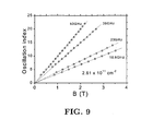
- Fig. 9 confirms the B-periodicity of the observed oscillations: the oscillation maxima have been assigned an integer index and their magnetic field position is plotted versus the index for various microwave frequencies. The electron density is equal to 2.61 x 10 11 /cm 2 .
- the influence of the microwave polarization has been investigated. Both for the photo-conductance and the photovoltaic effect, the amplitude of the oscillations was far stronger for a microwave electric field perpendicular to the current direction. For the photoconductance effect a threshold behaviour as a function of microwave power was observed. The threshold power value is lower for microwave radiation polarized perpendicular to the long direction of the Hall bar.
- the oscillation period was independent of temperature T, and the amplitude of the photoconductance oscillations only weakly drops upon increasing T from 1.5 to 10 K.
- the microwave power and the temperature dependencies of their amplitude were different.
- the amplitude of the photovoltaic oscillations is linear in the microwave power without a threshold and saturated at a value of approximately 2 mV for 0.1 mW of power. This value is close to the threshold power of the photoresistance oscillations.
- the spectral resolution of the device derived from direct measurements was about 1 - 2 GHz. In the experiment for the frequency range of about 20-50 GHz about 20-40 oscillations were observed. This gave a Q-factor and spectral resolution of about 1-2 GHz for the specific device used in these experiments.
- An additional parameter for controlling the period ⁇ B is the use of devices with different charge carrier density n s which can be easily varied from, say, 1 x 10 11 cm -2 (in a single quantum well) up to 1.5 x 10 12 cm -2 (for instance, in multiple quantum well systems with five quantum wells).
- Figs. 15 and 16 there is shown a first way of realising a 2D charge carrier layer in the form of an electron layer.
- the semiconductor structure comprises in this example a GaAs substrate 10, typically with a thickness of 0.3 to 0.5 mm (however, this is not critical).
- a GaAs buffer layer 12 is grown on the GaAs substrate and is followed by a superlattice structure 14 comprising alternating layers of AlGaAs and GaAs, with the AlGaAs layers typically being 7 nm thick and GaAs layers typically being 3 nm thick.
- the total thickness of the buffer structure 12, 14 typically amounts to 1 ⁇ m, however, this is again not critical. The idea is to prevent impurities from the GaAs substrate migrating into the active part of the device.
- the active part of the device comprises the layer 16 of GaAs (intrinsic material) which is followed by an intrinsic layer 18 of AlGaAs. After the intrinsic layer 18 has been grown it is followed by a silicon-doped AlGaAs layer 20 and a capping layer 22 of GaAs. If it is desired to change the density of electrons within one device, one can place an additional semitransparent conducting layer (not shown on the Figure) on top of the capping layer.
- the semitransparent conducting layer serves as a so-called top-gate: by applying a dc voltage between this layer and the 2DEG one can change the density of 2D electrons in the device.
- a semitransparent conducting top-gate for changing the density of the 2D electrons within the device by applying the voltage can be also added to systems shown in Figs. 17 and 20 below.
- an additional conducting layer, separated by at least one barrier from the 2DEG, may be inserted in the layer structure of Figs. 15, 17 and 20 below the 2D charge carrier layer (also not shown in the figures). It serves as a back-gate for changing the density of charge carriers in the 2DEG: applying a voltage between this back-gate and the 2DEG one can change the density of 2D electrons in the 2DEG.
- the structure is, for example, grown by molecular beam epitaxy, as are all other structures described here.
- the conduction band scheme for the structure of Fig. 15 is shown in Fig. 16.
- the potential well 24 has a quantised energy level 26 for electrons which are induced into the potential well by the silicon donor atoms provided in the layer 20. The electrons are thus sharply localised in the potential well 24 and this results in the two-dimensional electron gas illustrated as the layer 26 in Fig. 15.
- this two-dimensional electron gas is localised in the GaAs in a layer having a thickness of approximately 5-10 nm. Although this is a very thin layer it is probably better described as a quasi two-dimensional electron gas rather than a strict two-dimensional electron gas which would have zero thickness.
- the layers 18, 20 and 22 provided on top of the GaAs layer 16 have a total thickness typically in the range from 35 nm to 250 nm, with the relative proportions being as shown in the drawing. These dimensions are, however, not critical.
- the GaAs layer 16 typically has a thickness of approximately 1 ⁇ m, but again this is not critical.
- FIG. 17 there can be seen an alternative way of realising a two-dimensional electron gas.
- the structure of Fig. 17 is similar to that of Fig. 15 and the layers which are common to both structures have been given the same reference numerals.
- the layer 16 of GaAs has been reduced in this structure to a thin layer having a thickness of ⁇ 10 nm and that it is sandwiched between two layers 18 of intrinsic AlGaAs. These two layers 18 are in turn sandwiched between two layers 20 of AlGaAs doped with silicon.
- the conduction band diagram for this structure in the vicinity of the thin intrinsic GaAs layer 16 is shown in Fig. 18.
- the thin layer 16 of intrinsic GaAs forms the quantum well 24 with a quantised energy level 26 in which electrons are localised. The electrons are induced by the presence of the silicon donors in the two layers 20.
- Fig. 19 now shows how the semiconductor structure of Fig. 15 or Fig. 17 has been patterned in the shape of a Hall bar in order to provide a semiconductor structure which can be used for the purposes of the present invention.
- Fig. 15, or of Fig. 17 has been etched from the top in Fig. 15 (or Fig. 17) down to the GaAs layer 16 of Fig. 15 or down to the AlGaAs layer 18 beneath the GaAs layer 16 in Fig. 17, so that it has generally the shape of an H in plan view, with the crossbar 32 of the H being relatively broad relative to the "vertical" arms (34, 38, 34', 38') and with the crossbar being extended beyond the vertical arms of the H, so that the shape shown in perspective view in Fig. 19 results.
- the Hall bar schematically shown in Fig. 19 comprises the 2DEG layer 26, illustrated by a thick black line in Fig. 19, sandwiched between the intrinsic GaAs layer 16 of Fig. 15 (shown below the 2DEG 26) and the layer system 18, 20, 22 (shown above the 2DEG 26 in Fig. 15).
- the layer indicated as layer 16 in Fig. 19 would in fact comprise the layer 18 shown in Fig. 17 beneath the quantum well layer 16.
- contacts 46, 48 have been provided to the "uprights" 34 and 38 of the Hall bar at the "top” ends of the uprights and further contacts 46' and 48' have been provided to the “bottom” ends 34' and 38' of the "uprights", although these contacts are not exploited in this particular embodiment.
- contacts 54 and 56 are provided to the extensions 42 and 44 respectively of the crossbar 32 and are connected into a circuit 58 which drives a small current I between the two contacts 54 and 56, if photoresistance measurements are to be made. For photovoltaic or photocurrent measurements, no drive current is needed, and circuit 58 can be omitted.
- a circuit 59 for generating a magnetic field that may be tunable in magnitude and which extends perpendicular to the 2DEG 26, for example in the direction of the arrow 61, or has at least a field component extending in the direction of the arrow 61 (or in the opposite direction thereto).
- contacts 54 and 56 for passing a current through the device has the advantage that there is no current flowing between contacts 46 and 48, and as a result an uninteresting contribution (so called "contact resistance") from the interface between the potential contacts and the 2D charge layer itself is avoided.
- the magnetic field B can be held constant and the charge carrier density in the 2D charge carrier layer can be varied by varying the dc voltage between the semitransparent conducting top-gate and the 2DEG or between a conducting back-gate and the 2DEG. Again curves are obtained similar to those of Fig. 8a, Fig. 8b and Fig. 7 again allowing the frequency of the incident radiation and the amplitude thereof to be measured.
- the arrangement with sweeping magnetic field and a constant 2D charge carrier density (in one device realization) is more favourable because the top- or back-gate will partly screen (reflect) the incident electromagnetic radiation.
- An advantage of an additional dependency of the oscillation period on the 2D charge carrier density in the device can be fully used by using a plurality of devices with distinct but constant densities.
- Fig. 20 there can be seen another way of realising the semiconductor structure necessary for the device of the present invention.
- the structure is a double quantum well structure, which has two 2DEGs rather than just one, as in the embodiments of Fig. 15 and 17.
- the layer system is similar to that of Fig. 17 and therefore the same reference numerals are used to describe the layers as were used in Fig. 17.
- the band diagram of Fig. 21 that the shape of the conduction band essentially repeats the shape of the conduction band of Fig. 18 (for the semiconductor structure of Fig. 17).
- Fig. 20 could be replaced by a superlattice structure with alternating thin layers of GaAs and AlGaAs, so that a plurality of 2DEGs is present.
- Figs. 22 to 39 a variety of different schemes is shown for the shape of the 2D charge carrier layer and the contacting of this layer.
- Fig. 22 The simplest example is shown in Fig. 22 where the 2D charge carrier layer 26 is rectangular in shape and is provided with just two contacts 46 and 48 spaced apart by a distance L.
- the edge of the 2D charge carrier layer 26 between the contacts 46 and 48 is straight, this is the simplest conceivable detector configuration, and it is the contacts 46 and 48 which are responsible for the generation of the edge magnetoplasmons. Moreover these contacts allow to measure at least one of the photovoltage and photocurrent and photoresistance.
- Fig. 23 there can be seen an alternative embodiment in which the edge 62 of the 2D charge carrier layer 26 includes first and second projections 34, 38 and the first and second contacts 46, 48 are in this case respectively provided at said first and second projections.
- the projections 34, 38 can be additionally supplied by tunnel-barrier elements, as shown in Fig. 1c, for additional control of nonlinear behaviour of the contact regions. The same is valid for all similar elements in the subsequent figures.
- the device of Fig. 24 is essentially the same as that of Fig. 23 except that the distance L' between the first and second projections 34 and 38 is substantially larger than L in Fig. 23. Having regard to the equation 2, this signifies that the device of Fig. 24 is designed to detect a lower frequency than the device of Fig. 23.
- Fig. 25 shows a device similar to that of Fig. 23 with the first and second projections 34 and 38 being separated by the same distance L.
- the device of Fig. 25, however, also includes two further contacts 54 and 56 to the 2D charge carrier layer 26 and in practice a current is allowed to flow through an external circuit, such as 58 in Fig. 19 and between the contacts 54 and 56. Passing the external current between contacts 54 and 56 while measuring the photoresistance between contacts 46 and 48 allows one to avoid the influence of the undesired contact resistance, as described with respect to the embodiment of Fig. 19.
- Fig. 26 there can be seen a device which is essentially a combination of the device of Fig. 25 with that of Fig. 24.
- first and second projections 34 and 38, with contacts 46 and 48 are provided on one edge 62 of the 2D charge carrier layer 26, whereas third and fourth projections 34' and 38', with contacts 46' and 48', are provided at a second edge 64 of the 2D charge carrier layer 26, the second edge 64 being parallel to the opposite edge 62 in this example.
- two further contacts 54 and 56 are provided to the 2D charge carrier layer 26 and will be connected in practice to an external circuit such as 58 to avoid the influence of the contact resistance when measuring the photoresistance between the contacts 46 and 48 or the contacts 46' and 48'.
- This embodiment has the advantage that the effective separations L and L' between the respective pairs of contacts 46, 48 and 46', 48' are different, so that the same device can be used to detect electromagnetic radiation in different frequency bands, by taking measurements between contacts 46 and 48 for one frequency band and between contacts 46' and 48' for a second frequency band.
- Fig. 27 there can be seen an embodiment with three projections 34, 36, 38 and 34', 36' and 38' from each of two opposite edges 62 and 64.
- the spacing between the projections 34 and 36 is equal to L as is the spacing between the projections 36 and 38, between the projections 34' and 36' and between the projections 36' and 38'.
- any of the pairs of contacts 46 - 50, 50 - 48, 46' - 50', and 50' - 48' which are spaced apart by the distance L can be used to determine the presence of radiation, its frequency and intensity.
- the amplitude of the photovoltage/photocurrent/photoresistance oscillations is expected to increase the more contacts are present.
- edge 62, 64 between the contacts 46,48 or between the projections can be considered to be straight edges.
- Fig. 28 shows that this is not essential.
- the edge present between the projections 34 and 36 and between the projections 36 and 38 has the shape of a rectangular wave with further projections.
- the effect of these further projections 66, 68, 70, 66', 68', 70' is to enhance the generation of edge magnetoplasmons and to reduce the effective distance between the projections 34, 36 and 36, 38 by a number equivalent to the number of intermediate projections.
- the effective length L is now the distance between adjacent projections, so that the frequency range which the device is able to detect is correspondingly modified.
- the information about the frequency and the amplitude of the incident electromagnetic radiation will now be contained in the signal detected between the contacts 46 and 50, in the signal detected between contacts 50 and 48, as well as in the signal detected between the contacts 46 and 48.
- Fig. 30 shows a device where the three projections 34, 36 and 38 have different widths and wherein the effective spacing L between the pairs of contacts 50 and 48 differs from the effective spacing L' between the pair of contacts 46 and 50.
- the edge 62, 64 of the charge carrier layer 26 has either been straight between adjacent projections, such as 34, 36, 36, 38 and 38, 40, or has included a regularly repeating structure, such as the projections 66, 68, 70, 66', 68', 70', in the device of Fig. 28.
- the inhomogeneities at the edges 62 and/or 64 of the charge carrier layer 26 do not, however, have to be formed by straight lines or by regularly repeating structures. Instead, a wavy shape for the edge 62 also gives rise to inhomogeneities and Fig. 31 gives one example for an embodiment in which the inhomogeneities at the edge 62 are formed by a wavy shape of the edge. In the embodiment of Fig. 31 the wavy shape is regularly repeating with a periodic length of L which is the effective distance for the measurement of the frequency. However, the wavy shape of the edge does not have to be regular in shape or spatial periodicity.
- Fig. 32 shows an embodiment which corresponds largely to that of Fig. 28, but which has a different number of projections between the first pair of contacts 46 and 50 and between the second pair of contacts 48 and 52.
- the effective distance L between the contacts 46 and 50 differs from the effective distance L' between the contacts 48 and 52.
- the larger distance is more suitable for detecting low frequency radiation whereas the smaller distance is more appropriate for detecting high frequency oscillations.
- Fig. 33 shows that the inhomogeneities can, however, also be formed in a different way, in this case by one or more islands 69 of a 2D charge carrier layer dispersed apart between the first and second contacts 46 and 48 and generally opposite the edge 62.
- the separation between adjacent pairs of islands of the 2D charge carrier layer determines the effective frequency range which can be measured using this embodiment.
- the modulation of the edge of the 2D charge carrier layer has been described in terms of projections from the edge of the layer. It is, however, not necessary for inhomogeneities to be produced at the edge 62 or 64 of the 2D charge carrier layer by projections, they could instead be provided by indentations 70, 72, such as are shown in the embodiment of Fig. 34. It will be noted that the 2D charge carrier layer is contacted in this embodiment by contacts 74, 76 to the indentations in the edge 62 of the 2D charge carrier layer. Again, these indentations are separated by the effective distance L.
- Fig. 35 shows a device where the edge 62 of the 2D charge carrier layer 26 is provided with one projection 34 and one indentation 72, with the 2D charge carrier layer being contacted by contacts 46 and 76 to the projection 34 and to the indentation 72 respectively.
- the effective distance L between the projection 34 and the indentation 72 is the same as the effective distance L between the indentations 70 and 72 in Fig. 34.
- the projections or indentations have been provided at an outer edge 62 or 64 of the 2D charge carrier layer. They can, however, be realised differently as shown, for example, in the device of Fig. 36.
- the 2D charge carrier layer 26 has a central rectangular aperture 80 and the projections 34, 36, and 38 project inwardly from the 2D charge carrier layer into this aperture 80 at the edge 81.
- Respective contacts are provided to the projections as indicated as 46, 48 and 50.
- edge of the charge carrier layer need not necessarily take the form of projections into the aperture 80 of the 2D charge carrier layer but could also take the form of indentations of the edge 81 of the aperture (not shown in the drawing). Moreover, all the different topographies discussed above could also be adopted in the device of Fig. 36 and realised with respect to the edge 81 of the 2D charge carrier layer 26 defining the aperture.
- Fig. 37 shows, for example, a 2D charge carrier layer realised in the form of a circle or disk with projections extending from it.
- there are four projections 34, 36, 38 and 40 which are provided with contacts and one intermediate projection 90, 92, 94, 96 is respectively provided between each pair of projections (34, 36); (36, 38); (38, 40) and (40, 34) to which contacts are provided.
- the effective distance between each respective pair of contacts (46, 50); (50, 48); (48, 52) and (52, 46) is equivalent to L as a result of the presence of the projections 90, 92, 94, 96.
- the projections do not need to be spaced at equal angles around the centre of the disk, and there can be any number of projections or indentations between respective pairs of contacts.
- the topography of the edge between adjacent pairs of contacts can also be varied as desired. Topographies may be chosen on the basis of the examples given previously.
- Fig. 38 shows an embodiment similar to that of Fig. 37, but in which the projections 90, 92, 94 and 96 have been replaced by indentations 100, 102, 104 and 106.
- the effective separation between adjacent pairs of contacts (46, 50); (50, 48); (48, 52) and (52, 46) is again equal to L, so that the detector of Fig. 38 is configured for the same frequency range as the detector of Fig. 37.
- Fig. 39 shows that the disk can also be realised as a so-called Corbino disk, i.e. a circular disk with an aperture at the centre.
- Corbino disk i.e. a circular disk with an aperture at the centre.
- the contacts 46, 50, 48 and 52 to the outer edge of the disk are realised in precisely the same way as in the circular disk in Fig. 38 whereas the contacts 46', 48' to the inner edge of the Corbino disk, i.e. to the edge of the circular aperture in the disk of Fig. 39 are realised with a different effective separation between the two contacts shown, so that this device can be used to analyze the spectrum of incident radiation in two different frequency ranges for a given magnetic field and charge carrier density.
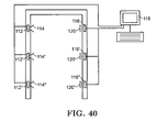
- Figs. 40 to 42 there are shown three illustrations of possible applications of the detector of the present invention.
- Fig. 40 shows a security portal 110 at a security terminal of an airport, train or bus station.
- sources 112, 112' and 112" of electromagnetic radiation provided at one side of the portal, each having a horn or antenna 114, 114', 114" for radiating the electromagnetic radiation across the security portal.
- a detector 116, 116', 116" Opposite to each horn is a detector 116, 116', 116" in accordance with the present invention and all three detectors are connected to a computer schematically illustrated as 118.
- a lens 120 (or a waveguide or a horn (not shown)) can be used to direct the electromagnetic radiation passing across the portal 110 and through a person walking through the portal 110 onto the detectors 116, 116', 116".
- Each detector is designed so that it can analyze the radiation in different frequency ranges during the time a person walks through the security portal.
- Each of the sources of electromagnetic radiation produces a spectrum of different frequencies, which have an enlarged absorption in or a different transmission through the plastic explosives or plastic weapons that may be carried by the person walking through the security portal. Analyzing the spectrum of the received radiation, the computer will then be able to determine whether the person walking through the security portal carries the plastic explosives/weapons or not.
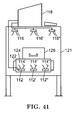
- Fig. 41 shows the same basic idea applied to an apparatus for testing passengers' luggage, the same reference numerals being used to designate parts common to Figs. 40 and 41.
- the luggage is moved through a tunnel 121 on a conveyor belt and sources of electromagnetic radiation 112, 112', 112" are provided within the loop 122 of the conveyor belt 124 and emit the radiation through respective horns 114, 114', 114" upwardly towards respective detectors 116, 116', 116" provided adjacent the top of the tunnel.
- the horns/antennas will emit electromagnetic radiation at frequencies which have an enlarged absorption in or a different transmission through the interested materials (for example plastic explosives or plastic weapons) and the detectors will be designed so that they can analyse the spectrum of the radiation received in corresponding frequency ranges, as explained above, so that all detectors can cover the entire frequency range or ranges of interest while a particular piece of luggage is passing beneath them.
- the detectors 116 being provided at the top of the tunnel 121 and the sources 112 of electromagnetic radiation within the loop of the conveyor belt.
- the sources of radiation 112 could be provided at the top of the tunnel 120 and the detectors 116 could be provided in the conveyor loop or the sources of electromagnetic radiation or the detectors 116 could be provided below the conveyor belt loop.
- the sources and detectors could be provided at opposite sides of the tunnel.
- the computer 118 is able to analyze the frequency spectrum of the electromagnetic radiation transmitted through a piece of luggage 126 and to determine whether there is a likelihood of plastic explosives or plastic weapons being hidden in the piece of luggage being investigated.
- Fig. 42 shows a system which is used to check for the presence of ill (for example cancerous) tissue.
- a tooth 128 in a gum 130 is shown and a source 112 of electromagnetic radiation is shown on one side of the tooth whereas a detector 116 for analysing the frequency spectrum of electromagnetic radiation transmitted through the investigated tissue is provided on the opposite side of the tooth.
- ill tissue for example cancerous tissue
- the system should be able to detect the tooth decay or cancerous growths in the gum. This is only one illustration of the application of the principle of detecting ill or cancerous tissue.
- the apparatus can be modified to detect cancerous tissue anywhere in the body, for example in the brain, in the colon, or in a patient's breasts.
- the described principle of detection of electromagnetic radiation can even be used without sources of radiation in Gigahertz/Terahertz frequency bands.
- the human body itself emits electromagnetic waves in the far-infrared range (Gigahertz and Terahertz frequency range)
- analyzing the spectrum of the emitted radiation and comparing the spectra emitted by a healthy person with the spectra emitted by an ill patient one could determine, at early stages, the development of different illnesses as for example cancer or liver illnesses.
- Detectors based on the described principle can also work in telecommunication applications.
- the present invention can be considered as a method of detecting the intensity and the frequency of electromagnetic radiation comprising:
- the method of the present invention can be considered as a method of detecting the intensity and the frequency of electromagnetic radiation comprising:
- the method of the present invention can be considered as a method of detecting the intensity and the frequency of electromagnetic radiation comprising:
Landscapes
- Chemical & Material Sciences (AREA)
- Engineering & Computer Science (AREA)
- Nanotechnology (AREA)
- Physics & Mathematics (AREA)
- Life Sciences & Earth Sciences (AREA)
- Biophysics (AREA)
- Optics & Photonics (AREA)
- Crystallography & Structural Chemistry (AREA)
- Photometry And Measurement Of Optical Pulse Characteristics (AREA)
- Light Receiving Elements (AREA)
- Measurement Of Radiation (AREA)
Applications Claiming Priority (2)
| Application Number | Priority Date | Filing Date | Title |
|---|---|---|---|
| US10/704,379 US6987484B2 (en) | 2003-11-07 | 2003-11-07 | Detector for electromagnetic radiation and a method of detecting electromagnetic radiation |
| US704379 | 2003-11-07 |
Publications (2)
| Publication Number | Publication Date |
|---|---|
| EP1530241A2 true EP1530241A2 (fr) | 2005-05-11 |
| EP1530241A3 EP1530241A3 (fr) | 2012-04-11 |
Family
ID=34435589
Family Applications (1)
| Application Number | Title | Priority Date | Filing Date |
|---|---|---|---|
| EP04026282A Withdrawn EP1530241A3 (fr) | 2003-11-07 | 2004-11-05 | Détecteur de radiations électromagnétiques et méthode de détection de radiations électromagnétiques |
Country Status (2)
| Country | Link |
|---|---|
| US (1) | US6987484B2 (fr) |
| EP (1) | EP1530241A3 (fr) |
Cited By (3)
| Publication number | Priority date | Publication date | Assignee | Title |
|---|---|---|---|---|
| CN108761220A (zh) * | 2018-08-13 | 2018-11-06 | 苏州特拉芯光电技术有限公司 | 一种太赫兹天线机器人近场三合一测试系统 |
| CN112198468A (zh) * | 2020-09-11 | 2021-01-08 | 中国科学院金属研究所 | 一种波导法微波介质材料超低温复电磁参数测试装置 |
| CN113097035A (zh) * | 2021-03-05 | 2021-07-09 | 北京大学 | 一种人工局域表面等离激元回旋电子激射器及其实现方法 |
Families Citing this family (12)
| Publication number | Priority date | Publication date | Assignee | Title |
|---|---|---|---|---|
| US7705415B1 (en) * | 2004-08-12 | 2010-04-27 | Drexel University | Optical and electronic devices based on nano-plasma |
| US7598919B2 (en) * | 2006-01-12 | 2009-10-06 | Lockheed Martin Corporation | Pick-up horn for high power thermal vacuum testing of spacecraft payloads |
| US7750859B2 (en) * | 2006-01-12 | 2010-07-06 | Lockheed Martin Corporation | Generic pick-up horn for high power thermal vacuum testing of satellite payloads at multiple frequency bands and at multiple polarizations |
| US8497527B2 (en) * | 2008-03-12 | 2013-07-30 | Sensor Electronic Technology, Inc. | Device having active region with lower electron concentration |
| DE102008002270A1 (de) * | 2008-06-06 | 2009-12-17 | Robert Bosch Gmbh | Multispektraler Sensor |
| EP2190022B1 (fr) * | 2008-11-20 | 2013-01-02 | Hitachi Ltd. | Dispositif de transport de charge à polarisation du spin |
| US7751112B2 (en) | 2008-12-09 | 2010-07-06 | The Invention Science Fund I, Llc | Magnetic control of surface states |
| US8000062B2 (en) | 2008-12-30 | 2011-08-16 | Hitachi Global Storage Technologies Netherlands B.V. | Enhanced magnetoresistance and localized sensitivity by gating in lorentz magnetoresistors |
| US9329339B2 (en) * | 2009-09-02 | 2016-05-03 | Agency For Science, Technology And Research | Plasmonic detector and method for manufacturing the same |
| US8159667B2 (en) * | 2009-12-10 | 2012-04-17 | Terasense Group, Inc. | Tera- and gigahertz solid state miniature spectrometer |
| JP5371053B2 (ja) * | 2010-05-24 | 2013-12-18 | 日本電信電話株式会社 | 高周波素子 |
| US9297638B1 (en) * | 2014-10-21 | 2016-03-29 | Sandia Corporation | Two-path plasmonic interferometer with integrated detector |
Citations (2)
| Publication number | Priority date | Publication date | Assignee | Title |
|---|---|---|---|---|
| US4353070A (en) | 1979-08-01 | 1982-10-05 | Agence Nationale De Valorization De La Recherche | Broad band system operating in the submillimeter wave range |
| US5914497A (en) | 1997-07-14 | 1999-06-22 | Sherwin; Mark | Tunable antenna-coupled intersubband terahertz (TACIT) detector |
Family Cites Families (9)
| Publication number | Priority date | Publication date | Assignee | Title |
|---|---|---|---|---|
| US4399442A (en) * | 1981-07-06 | 1983-08-16 | The United States Of America As Represented By The Secretary Of The Army | Active transmitting antenna employing an electron beam bombarded semiconductor |
| US6316771B1 (en) * | 1981-07-13 | 2001-11-13 | Lockhead Martin Corp. | Superlattice tunable detector system |
| USH95H (en) * | 1985-11-27 | 1986-07-01 | United States Of America | Heterojunction D- (or A+) millimeter and submillimeter wave detector |
| US4940898A (en) * | 1986-09-30 | 1990-07-10 | Colorado State University Research Foundation | Semiconducting metal silicide radiation detectors |
| US5079601A (en) * | 1989-12-20 | 1992-01-07 | International Business Machines Corporation | Optoelectronic devices based on intraband transitions in combinations of type i and type ii tunnel junctions |
| DE4101389C2 (de) * | 1991-01-18 | 1994-03-17 | Max Planck Gesellschaft | Verfahren zur Messung elektromagnetischer Strahlung, Halbleiter-Strahlungsdetektor zur Durchführung des Verfahrens und Verfahren zur Herstellung eines Halbleiter-Strahlungsdetektors |
| US5459343A (en) * | 1992-02-21 | 1995-10-17 | Texas Instruments Incorporated | Back gate FET microwave switch |
| WO1994023470A1 (fr) * | 1993-03-26 | 1994-10-13 | Superconductor Technologies, Inc. | Amplificateur faible bruit |
| US6476596B1 (en) * | 1999-12-06 | 2002-11-05 | The United States Of America As Represented By The Secretary Of The Army | Method and apparatus for detection of terahertz electric fields using polarization-sensitive excitonic electroabsorption |
-
2003
- 2003-11-07 US US10/704,379 patent/US6987484B2/en not_active Expired - Fee Related
-
2004
- 2004-11-05 EP EP04026282A patent/EP1530241A3/fr not_active Withdrawn
Patent Citations (2)
| Publication number | Priority date | Publication date | Assignee | Title |
|---|---|---|---|---|
| US4353070A (en) | 1979-08-01 | 1982-10-05 | Agence Nationale De Valorization De La Recherche | Broad band system operating in the submillimeter wave range |
| US5914497A (en) | 1997-07-14 | 1999-06-22 | Sherwin; Mark | Tunable antenna-coupled intersubband terahertz (TACIT) detector |
Non-Patent Citations (15)
| Title |
|---|
| "NATO Science Series II", MATHEMATICS, PHYSICS AND CHEMISTRY, pages 187 - 207 |
| A. L. FETTER, PHYS. REV. B, vol. 32, 1985, pages 7676 |
| M. DYAKONOV; M. S. SHUR: "Terahertz Sources and Systems", vol. 27, 2001, KLUVER |
| M. I. DYAKONOV; M. SHUR, IEEE TRANS. ELECTRON. DEV., vol. 43, 1996, pages 380 |
| P.J. M. PETERS; M. J. LEA; A. M. L. JANSSEN; A. O. STONE; W. P. N. M. JACOBS; P. FOZOONI; R. W. VAN DER HEIJDEN, PHYS. REV. LETT., vol. 67, 1991, pages 2199 |
| S. A. MIKHAILOV: "Edge Excitations of Low-Dimensional Charged Systems", 2000, NOVA SCIENCE PUBLISHERS, INC. |
| SOV. PHYS.-JETP, vol. 67, 1988, pages 1639 - 1653 |
| T. W. CROW; R. J. MATTAUCH; R. M. WEIKLE; U. V. BHAPKAR: "Compound Semiconductor Electronics", 1996, WORLD SCIENTIFIC |
| V. A. VOLKOV; S. A. MIKHAILOV, ZH. EKSP. TEOR. FIZ., vol. 94, 1988, pages 217 |
| V. A. VOLKOV; S. A. MIKHAILOV: "Landau Level Spectroscopy", vol. 27.2, 1991, pages: 855 - 907 |
| W. KNAP; V. KACHOROVSKII; Y. DENG; S. RUMYANTSEV; J.-Q. LII; R. GASKA; M. S. SHUR; G. SIMIN; X. HU; M. A. KHAN ET AL., APPL. PHYS., vol. 80, 2002, pages 3433 |
| W. KNAP; V. KACHOROVSKII; Y. DENG; S. RUMYANTSEV; J.-Q. LII; R. GASKA; M. S. SHUR; G. SIMIN; X. HU; M. A. KHAN ET AL., J. APPL. PHYS., vol. 91, 2002, pages 9346 |
| W. KNAP; Y. DENG; S. RUMYANTSEV; J.-Q. LII; M. S. SHUR; C. A. SAYLOR; L. C. BRUNEL, APPL. PHYS. LETT., vol. 80, 2002, pages 3433 |
| W. KNAP; Y. DENG; S. RUMYANTSEV; M. S. SHUR, APPL. PHYS. LETT., vol. 81, 2002, pages 4637 |
| X. G. PERALTA; S. J. ALLEN; M. C. WANKE; N. E. HARFF; J. A. SIMMONS; M. P. LILLY; J. L. RENO; P. J. BURKE; J. P. EISENSTEIN, APPL. PHYS. LETT., vol. 81, 2002, pages 1627 |
Cited By (4)
| Publication number | Priority date | Publication date | Assignee | Title |
|---|---|---|---|---|
| CN108761220A (zh) * | 2018-08-13 | 2018-11-06 | 苏州特拉芯光电技术有限公司 | 一种太赫兹天线机器人近场三合一测试系统 |
| CN112198468A (zh) * | 2020-09-11 | 2021-01-08 | 中国科学院金属研究所 | 一种波导法微波介质材料超低温复电磁参数测试装置 |
| CN113097035A (zh) * | 2021-03-05 | 2021-07-09 | 北京大学 | 一种人工局域表面等离激元回旋电子激射器及其实现方法 |
| CN113097035B (zh) * | 2021-03-05 | 2021-12-28 | 北京大学 | 一种人工局域表面等离激元回旋电子激射器及其实现方法 |
Also Published As
| Publication number | Publication date |
|---|---|
| US6987484B2 (en) | 2006-01-17 |
| US20050099345A1 (en) | 2005-05-12 |
| EP1530241A3 (fr) | 2012-04-11 |
Similar Documents
| Publication | Publication Date | Title |
|---|---|---|
| US8159667B2 (en) | Tera- and gigahertz solid state miniature spectrometer | |
| US6987484B2 (en) | Detector for electromagnetic radiation and a method of detecting electromagnetic radiation | |
| US7420225B1 (en) | Direct detector for terahertz radiation | |
| US8772890B2 (en) | Apparatus and method of detecting electromagnetic radiation | |
| Ahi | Review of GaN-based devices for terahertz operation | |
| Watanabe et al. | InP-and GaAs-based plasmonic high-electron-mobility transistors for room-temperature ultrahigh-sensitive terahertz sensing and imaging | |
| US9297638B1 (en) | Two-path plasmonic interferometer with integrated detector | |
| Khiabani | Modelling, design and characterisation of terahertz photoconductive antennas | |
| US11114738B2 (en) | Tunable resonant circuit comprising a RF resonator geometry disposed on an active material layer such that resonance changes when photon energy is applied | |
| US20050093023A1 (en) | Frequency selective terahertz radiation detector | |
| Kukushkin et al. | Miniature quantum-well microwave spectrometer operating at liquid-nitrogen temperatures | |
| Kawano | Highly sensitive detector for on-chip near-field THz imaging | |
| JPH06109534A (ja) | エッジチャネルに断熱輸送を生じる半導体素子 | |
| Bhatti et al. | Spatially resolved Raman scattering from hot acoustic and optic plasmons | |
| Xia et al. | Experimental realization of a metasurface-based PETS THz detector | |
| Jaidl | Towards broadband terahertz quantum cascade ring laser frequency combs | |
| RU2816104C1 (ru) | Детектор электромагнитного излучения | |
| Sahafi | Terahertz radiation effects in quantum systems | |
| But | Silicon based terahertz radiation detectors | |
| Mikhailov et al. | New physical principle of detecting electromagnetic radiation | |
| Khanal | Quantum Cascade Lasers for Terahertz Applications | |
| HK1185416A (en) | Tera-and gigahertz solid state miniature spectrometer | |
| Quispe | Terahertz Characterization of III-Nitride Compound Semiconductors and Novel Device Structures | |
| Zhao | Novel terahertz devices based on intersubband transitions in quantum wells | |
| Gornik et al. | Wire and Dot Related Devices |
Legal Events
| Date | Code | Title | Description |
|---|---|---|---|
| PUAI | Public reference made under article 153(3) epc to a published international application that has entered the european phase |
Free format text: ORIGINAL CODE: 0009012 |
|
| AK | Designated contracting states |
Kind code of ref document: A2 Designated state(s): AT BE BG CH CY CZ DE DK EE ES FI FR GB GR HU IE IS IT LI LU MC NL PL PT RO SE SI SK TR |
|
| AX | Request for extension of the european patent |
Extension state: AL HR LT LV MK YU |
|
| RAP3 | Party data changed (applicant data changed or rights of an application transferred) |
Owner name: MAX-PLANCK-GESELLSCHAFT ZUR FOERDERUNG DER WISSENS |
|
| PUAL | Search report despatched |
Free format text: ORIGINAL CODE: 0009013 |
|
| AK | Designated contracting states |
Kind code of ref document: A3 Designated state(s): AT BE BG CH CY CZ DE DK EE ES FI FR GB GR HU IE IS IT LI LU MC NL PL PT RO SE SI SK TR |
|
| AX | Request for extension of the european patent |
Extension state: AL HR LT LV MK YU |
|
| RIC1 | Information provided on ipc code assigned before grant |
Ipc: H01L 27/144 20060101ALI20120307BHEP Ipc: H01L 31/101 20060101ALI20120307BHEP Ipc: H01L 31/0352 20060101AFI20120307BHEP |
|
| 17P | Request for examination filed |
Effective date: 20120718 |
|
| 17Q | First examination report despatched |
Effective date: 20120806 |
|
| AKX | Designation fees paid |
Designated state(s): AT BE BG CH CY CZ DE DK EE ES FI FR GB GR HU IE IS IT LI LU MC NL PL PT RO SE SI SK TR |
|
| STAA | Information on the status of an ep patent application or granted ep patent |
Free format text: STATUS: THE APPLICATION IS DEEMED TO BE WITHDRAWN |
|
| 18D | Application deemed to be withdrawn |
Effective date: 20140603 |