EP1530233A2 - Semiconductor device and method of manufacturing the same - Google Patents
Semiconductor device and method of manufacturing the same Download PDFInfo
- Publication number
- EP1530233A2 EP1530233A2 EP04026578A EP04026578A EP1530233A2 EP 1530233 A2 EP1530233 A2 EP 1530233A2 EP 04026578 A EP04026578 A EP 04026578A EP 04026578 A EP04026578 A EP 04026578A EP 1530233 A2 EP1530233 A2 EP 1530233A2
- Authority
- EP
- European Patent Office
- Prior art keywords
- layer
- forming
- trench
- semiconductor device
- isolation trench
- Prior art date
- Legal status (The legal status is an assumption and is not a legal conclusion. Google has not performed a legal analysis and makes no representation as to the accuracy of the status listed.)
- Withdrawn
Links
Images



Classifications
-
- H—ELECTRICITY
- H10—SEMICONDUCTOR DEVICES; ELECTRIC SOLID-STATE DEVICES NOT OTHERWISE PROVIDED FOR
- H10W—GENERIC PACKAGES, INTERCONNECTIONS, CONNECTORS OR OTHER CONSTRUCTIONAL DETAILS OF DEVICES COVERED BY CLASS H10
- H10W10/00—Isolation regions in semiconductor bodies between components of integrated devices
- H10W10/01—Manufacture or treatment
- H10W10/011—Manufacture or treatment of isolation regions comprising dielectric materials
- H10W10/014—Manufacture or treatment of isolation regions comprising dielectric materials using trench refilling with dielectric materials, e.g. shallow trench isolations
-
- H—ELECTRICITY
- H10—SEMICONDUCTOR DEVICES; ELECTRIC SOLID-STATE DEVICES NOT OTHERWISE PROVIDED FOR
- H10W—GENERIC PACKAGES, INTERCONNECTIONS, CONNECTORS OR OTHER CONSTRUCTIONAL DETAILS OF DEVICES COVERED BY CLASS H10
- H10W10/00—Isolation regions in semiconductor bodies between components of integrated devices
- H10W10/01—Manufacture or treatment
- H10W10/011—Manufacture or treatment of isolation regions comprising dielectric materials
- H10W10/014—Manufacture or treatment of isolation regions comprising dielectric materials using trench refilling with dielectric materials, e.g. shallow trench isolations
- H10W10/0145—Manufacture or treatment of isolation regions comprising dielectric materials using trench refilling with dielectric materials, e.g. shallow trench isolations of trenches having shapes other than rectangular or V-shape
-
- H—ELECTRICITY
- H10—SEMICONDUCTOR DEVICES; ELECTRIC SOLID-STATE DEVICES NOT OTHERWISE PROVIDED FOR
- H10W—GENERIC PACKAGES, INTERCONNECTIONS, CONNECTORS OR OTHER CONSTRUCTIONAL DETAILS OF DEVICES COVERED BY CLASS H10
- H10W10/00—Isolation regions in semiconductor bodies between components of integrated devices
- H10W10/01—Manufacture or treatment
- H10W10/041—Manufacture or treatment of isolation regions comprising polycrystalline semiconductor materials
-
- H—ELECTRICITY
- H10—SEMICONDUCTOR DEVICES; ELECTRIC SOLID-STATE DEVICES NOT OTHERWISE PROVIDED FOR
- H10W—GENERIC PACKAGES, INTERCONNECTIONS, CONNECTORS OR OTHER CONSTRUCTIONAL DETAILS OF DEVICES COVERED BY CLASS H10
- H10W10/00—Isolation regions in semiconductor bodies between components of integrated devices
- H10W10/10—Isolation regions comprising dielectric materials
- H10W10/17—Isolation regions comprising dielectric materials formed using trench refilling with dielectric materials, e.g. shallow trench isolations
-
- H—ELECTRICITY
- H10—SEMICONDUCTOR DEVICES; ELECTRIC SOLID-STATE DEVICES NOT OTHERWISE PROVIDED FOR
- H10W—GENERIC PACKAGES, INTERCONNECTIONS, CONNECTORS OR OTHER CONSTRUCTIONAL DETAILS OF DEVICES COVERED BY CLASS H10
- H10W10/00—Isolation regions in semiconductor bodies between components of integrated devices
- H10W10/40—Isolation regions comprising polycrystalline semiconductor materials
Definitions
- the present invention relates to a semiconductor device and a method of manufacturing the same.
- a semiconductor device is provided with circuit elements such as a transistor, a resistance, a condenser and the like disposed on a semiconductor substrate, and the circuit elements are connected to one another via an interconnect for executing an instructed circuit operation, to thereby perform a function as required.
- the circuit elements have to be electrically insulated in order to effectively perform the circuit operation and function. Accordingly, various insulating and isolating techniques have been proposed, such as a trench isolation technique of filling a layer in a trench formed on a semiconductor substrate. A conventional example of a method of manufacturing a semiconductor device utilizing a trench isolation technique is described hereunder.
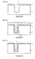
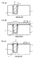
- Figs. 7A to 8C are schematic cross-sectional views showing a conventional method of manufacturing a semiconductor device.
- a mask oxide layer 2 having an opening of 0.5 to 2 ⁇ m in width is formed in a thickness of 100 to 600 nm on a silicon substrate 1. Then an anisotropic etching is performed on the silicon substrate 1 utilizing the mask oxide layer 2 as an etching mask, so that a trench 3 of 1 to 5 ⁇ m in depth is formed on the silicon substrate 1.
- the trench 3 is to serve as an isolation trench.
- the mask oxide layer 2 is removed, and a silicon oxide layer is formed in a thickness of 100 to 800 nm over a surface of the silicon substrate 1 and the trench 3 by a thermal oxidation process.
- This silicon oxide layer serves as a dielectric layer 4.
- a polycrystalline silicon layer is formed in a thickness of 150 to 1500 nm on the dielectric layer 4, for example by a CVD (Chemical Vapor Deposition) process, so that the trench 3 is filled with the polycrystalline silicon layer, to thereby constitute a trench isolation region 33.
- the polycrystalline silicon layer that is filled in the trench 3 will be herein referred to as a filling polycrystalline silicon layer 5.
- a layer formed by a CVD process will be herein referred to as a CVD layer.
- etch-back or a CMP (Chemical and Mechanical Polishing) process is performed so as to remove the filling polycrystalline silicon layer 5 except a portion formed in the trench isolation region 33.
- a wet etching is performed so as to remove the dielectric layer 4 except a portion formed in the trench 3.
- a gate insulating layer 6 of a transistor is formed in a thickness of 3 to 30 nm on a surface of the silicon substrate 1 and the trench isolation region 33 by a CVD process, and a polycrystalline silicon layer is formed thereon in a thickness of 100 to 600 nm by a CVD process.
- a conductive impurity is diffused in the polycrystalline silicon layer, so as to constitute an impurity-diffused polycrystalline silicon layer 7.
- a resist defining a gate electrode pattern 14 is formed by a known lithography technique, after which an anisotropic etching is performed to form a gate electrode 8 constituted of the impurity-diffused polycrystalline silicon layer 7, and then the resist is removed as shown in Fig. 8C.
- JP-A Laid Open No. 2002-237518 and others disclose a method of reducing a recess formed in the trench isolation region.
- the etching for removing the dielectric layer 4 often overpasses a surface of the silicon substrate 1 and the filling polycrystalline silicon layer 5 in the wet etching performed in the process according to Fig. 8A. For this reason a gap A is prone to be formed between the dielectric layer 4 and the surface of the silicon substrate 1, and likewise a gap B is prone to be formed between the dielectric layer 4 and the filling polycrystalline silicon layer 5.
- the gate insulating layer 6 does not fill an entire portion of the trench between the gap A and the gap B, but instead forms a uniform layer along a shape of the gaps, thereby preserving a recessed shape of the trench. Therefore, though the anisotropic etching is performed to remove the impurity-diffused polycrystalline silicon layer 7, a sufficient etching effect cannot be achieved in the proximity of a bottom portion of the trench, which is coated with the gate insulating layer 6, and resultantly an etching residue 9 of the impurity-diffused polycrystalline silicon layer 7 often remains unremoved.
- the etching residue 9 may be peeled off and freely float in a solution, for example in a cleaning process, to later stick to a surface of silicon substrate 1 as a waste. And such waste stuck to the surface of the silicon substrate 1 is prone to cause an abnormality in a characteristic of a semiconductor device, to thereby degrade reliability of the device. Also, a waste floating in a solution of a cleaning device may also stick to a surface of another silicon substrate, while the cleaning device is processing that silicon substrate. Further, the etching residue 9 may also freely float in the device because of a heat treatment, a CVD process or an ion implantation process, in addition to the cleaning process.
- JP-A Laid Open No. 2002-237518 permits reducing a size of a recess formed in a trench isolation region, however cannot completely eliminate the recess, and therefore has not reached a solution of the problem of the waste from the etching residue. Besides, the problem of the waste from the etching residue may still be incurred even when the recess or the gap is very small.
- the present invention has recognized in view of the foregoing problem, and there is provided a technique through which reliability of a semiconductor device can be upgraded.
- a semiconductor device comprising a semiconductor substrate; an isolation trench formed inside the semiconductor substrate; a first layer formed along an inner wall of the isolation trench so as to constitute a lining; a second layer formed in contact with an inner surface of the first layer so as to fill the isolation trench; and a conductive layer selectively formed on the isolation trench so as to cover the first layer and the second layer.
- a conductive layer is selectively provided so as to cover the first layer and the second layer. Such structure prevents emergence of an etching residue on second layer. Therefore, reliability of a semiconductor device can be upgraded.
- a method of manufacturing a semiconductor device comprising forming an isolation trench having a predetermined depth from a surface of a semiconductor substrate; forming a dielectric layer on the surface of the semiconductor substrate including the isolation trench; filling the isolation trench with a CVD layer; removing the dielectric layer except a portion in the isolation trench by an etching; sequentially forming an insulating layer and a conductive layer; forming a resist defining a pattern which covers via the conductive layer a portion of the insulating layer in contact with the dielectric layer; and performing an anisotropic etching on the resist to thereby remove a portion of the conductive layer exposing a surface thereof.
- the pattern covering a portion of the insulating layer in contact with the dielectric layer is constituted of a conductive layer. Accordingly, performing an etching to remove the dielectric layer except a portion in the isolation trench permits suppressing emergence of an etching residue on the insulating layer which is in contact with the dielectric layer, even though a gap is formed between at least either the semiconductor substrate or the CVD layer and the dielectric layer. Therefore, a highly reliable semiconductor device can be stably manufactured.
- a method of manufacturing a semiconductor device comprising forming an isolation trench on an upper portion of a semiconductor substrate; forming a first layer in contact with an upper surface of the semiconductor substrate including an inner wall of the isolation trench; filling the isolation trench with a second layer; selectively removing the first layer except a portion in the isolation trench; forming an insulating layer so as to cover the first layer, the second layer and an upper surface of the semiconductor substrate; forming a conductive layer so as to cover an upper surface of the insulating layer; forming a resist defining a pattern which covers via the conductive layer a portion of the insulating layer in contact with the second layer and with the first layer; and selectively removing an exposed portion of the conductive layer and forming a gate electrode, and a conductive layer on top of the isolation trench.
- the conductive layer is formed in contact with an upper surface of the insulating layer. Therefore, selectively removing the first layer except a portion in the isolation trench permits preventing emergence of an etching residue of the conductive layer on the insulating layer in contact with the first layer. Consequently, a highly reliable semiconductor device can be stably manufactured.
- the method of manufacturing a semiconductor device according to the present invention permits preventing emergence of an etching residue of the conductive layer provided for forming a gate electrode, and therefore contributes to upgrade reliability of a semiconductor device.
- a method of manufacturing a semiconductor device according to the present invention is to utilize a conductive layer for forming a gate electrode in constituting a pattern to cover a portion of a trench isolation region where waste is prone to be produced.
- the resist may be provided with a pattern for forming a gate electrode of a transistor.
- the resist is provided with a pattern for forming a gate electrode of a transistor, a conductive layer pattern for preventing emergence of an etching residue is formed during a formation process of the gate electrode. This method minimizes the need to add a process to eliminate the gap and a process to remove an etching residue.
- the resist may cover via the conductive layer a portion of the insulating layer in contact with the CVD layer.
- the pattern covering a portion of the insulating layer in contact with the CVD layer is constituted of the conductive layer, emergence of an etching residue on the insulating layer in contact with the CVD layer can be prevented.
- the CVD layer may be a polycrystalline silicon layer.
- the CVD layer to fill the isolation trench is a polycrystalline silicon layer, filling performance is improved compared with other CVD layers.
- the CVD layer may be constituted of a same material as the dielectric layer.
- the CVD layer to fill the isolation trench and the dielectric layer are of the same material, formation of a gap between the CVD layer and the dielectric layer can be prevented.
- the dielectric layer may be a silicon oxide layer.
- the dielectric layer is a silicon oxide layer. Accordingly, even though the isolation trench is filled with a polycrystalline silicon layer, an entirety of the layers provided in the trench can remain insulated. Particularly, in case where the CVD layer filled in the isolation trench is a silicon oxide layer which is the same as the dielectric layer, the insulation performance is improved, which facilitates forming a finer isolation trench and thereby further micronizing the semiconductor device.
- a semiconductor device 100 according to a first embodiment will be described.
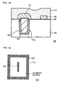
- Fig. 1A is a schematic cross-sectional view showing a constitution of a semiconductor device 100 according to this embodiment.
- Fig. 1B is a schematic plan view showing a constitution of a semiconductor device 100 according to this embodiment.
- a constitution of a circuit element such as a transistor and the like will be omitted from the drawing, along with a detailed description thereof.
- the semiconductor device 100 has such a structure that a trench shield 115 (conductive layer) constituted of a conductive impurity-diffused polycrystalline silicon layer is provided over a trench isolation region 113 formed on a silicon substrate 101, via a gate insulating layer 106. Also, a gate electrode 108 is provided on a gate insulating layer 106, and the trench shield 115 and the gate electrode 108 are constituted of a portion of the same impurity-diffused polycrystalline silicon layer.
- An interlayer dielectric layer 117 is provided on the trench shield 115 and the gate electrode 108 for insulation between circuit elements and interconnects. On the interlayer dielectric layer 117, an interconnect (not shown in the drawings) is disposed for connection between circuit elements.
- the semiconductor device 100 is constituted of the silicon substrate 101 (semiconductor substrate) including the trench isolation region 113 which is an isolation trench having a predetermined depth from an upper surface of the silicon substrate 101, the gate insulating layer 106, the gate electrode 108, the trench shield 115 and the interlayer dielectric layer 117.
- a dielectric layer 104 such as a silicon oxide layer is provided in contact with an inner wall of the trench isolation region 113 in a form of a lining
- a filling polycrystalline silicon layer 105 (second layer) is provided in contact with an inner face of the dielectric layer 104 so as to fill the trench isolation region 113.
- the gate insulating layer 106 is formed so as to cover the silicon substrate 101, the dielectric layer 104, and the filling polycrystalline silicon layer 105. Now, as shown in Fig. 1A, since there is a gap between the dielectric layer 104 and the filling polycrystalline silicon layer 105, the gate insulating layer 106 has a recess where the gap exists.
- the gate electrode 108 and the trench shield 115 are provided on the gate insulating layer 106.
- the trench shield 115 is located so as to cover the dielectric layer 104 and the filling polycrystalline silicon layer 105, which are selectively formed on the trench isolation region 113.
- the gate insulating layer 106 is provided over a region including a first region where the trench shield 115 is provided and a second region where the gate electrode 108 is provided, and the gate insulating layer 106 insulates the trench shield 115 from the dielectric layer 104 and filling polycrystalline silicon layer 105 to be later described, in the first region. In the second region, the gate insulating layer 106 insulates the gate electrode 108 from the silicon substrate 101 to be later described.
- a height from the gate insulating layer 106 to an upper face of the trench shield 115 and a height from the gate insulating layer 106 to an upper face of the gate electrode 108 are substantially the same.
- Figs. 2A to 4C are schematic cross-sectional views showing a method of manufacturing a semiconductor device according to this embodiment.
- a mask oxide layer 102 having an opening of 0.5 to 2 ⁇ m in width is formed in a thickness of 100 to 600 nm on the silicon substrate 101. Then an anisotropic etching is performed on the silicon substrate 101 utilizing the mask oxide layer 102 as an etching mask, so that a trench 103 of 1 to 5 ⁇ m in depth is formed on the silicon substrate 101.
- the trench 103 is to serve as an isolation trench.
- the mask oxide layer 102 is removed, and a silicon oxide layer is formed as the dielectric layer 104 in a thickness of 100 to 800 nm over the silicon substrate 101 and an inner wall of the trench 103, for example by a thermal oxidation process.
- a polycrystalline silicon layer is formed in a thickness of 150 to 1500 nm on the dielectric layer 104 by a CVD (Chemical Vapor Deposition) process, so that the trench 103 is filled with the polycrystalline silicon layer, to thereby constitute a trench isolation region 133.
- CVD Chemical Vapor Deposition
- a reason of forming the layer that is filled the trench 103 by a CVD process in this embodiment is that the CVD process permits efficiently forming a layer which is conformal to an underlying layer and also offers an excellent filling performance into a groove.
- the polycrystalline silicon layer that is filled in the trench 103 will be herein referred to as a filling polycrystalline silicon layer 105.
- a layer formed by a CVD process will be herein referred to as a CVD layer.
- an etch-back or a CMP (Chemical and Mechanical Polishing) process is performed so as to remove the filling polycrystalline silicon layer 105 except a portion formed in the trench isolation region 133.
- a wet etching is performed so as to remove the dielectric layer 104 except a portion formed in the trench 103.
- the gate insulating layer 106 of a transistor is formed in a thickness of 3 to 30 nm on an upper surface of the silicon substrate 101 and the trench isolation region 133, for example by a CVD process. Then a polycrystalline silicon layer is formed in a thickness of 100 to 600 nm in contact with an upper surface of the gate insulating layer 106, for example by a CVD process.
- a conductive impurity is diffused in the polycrystalline silicon layer, so as to constitute an impurity-diffused polycrystalline silicon layer 107.
- a resist 110 is formed on the impurity-diffused polycrystalline silicon layer 107 (Fig. 4A). Then an isolation region pattern 112 to cover the trench isolation region 113 and a gate electrode pattern 114 are formed by a known lithography technique, utilizing the resist 110 (Fig. 4B).
- the isolation region pattern 112 is located so as to cover a portion of the gate insulating layer 106 provided along a recess designated as a gap A and a gap B in Fig. 3B, via the impurity-diffused polycrystalline silicon layer 107.
- an anisotropic etching is performed on the isolation region pattern 112 and the gate electrode pattern 114 defined by the resist 110, to remove a portion of the impurity-diffused polycrystalline silicon layer 107 exposing a surface thereof.
- an anisotropic etching is performed on the isolation region pattern 112 and the gate electrode pattern 114 defined by the resist 110, to remove a portion of the impurity-diffused polycrystalline silicon layer 107 exposing a surface thereof.
- the gate electrode 108 and the trench shield 115 which covers the trench isolation region 113 are formed at a time in the same single process, out of the same impurity-diffused polycrystalline silicon layer 107.
- an impurity diffusion is performed on the silicon substrate 101 to form a source electrode and a drain electrode of the transistor, and the interlayer dielectric layer 117 shown in Fig. 1A is formed, after which circuit elements such as a condenser and the like are formed, and then an interconnect is formed to achieve a connection between the circuit elements.
- a portion of the gate insulating layer 106 that is in contact with the dielectric layer 104 in the trench isolation region 113 is covered with the trench shield 115.
- Such constitution prevents the impurity-diffused polycrystalline silicon layer 107 on the dielectric layer 104 from being peeled off to turn into a waste when forming the gate electrode 108.
- the advantage of this embodiment is prominently exhibited.
- the impurity-diffused polycrystalline silicon layer 107 constituting the trench shield 115 provided on the trench isolation region 113 as shown in Fig. 1B is electrically insulated from the surrounding circuit elements, and is therefore inhibited from causing undesired influence to an electrical characteristic or reliability of the semiconductor device.
- an area where the trench shield 115 makes contact with the gate insulating layer 106 only becomes slightly larger than an area of an upper surface of trench isolation region 113. Therefore, a reduced amount of a conductive layer can constitute the device, compared with a case where the conductive layer constituting the gate electrode is extended so as to cover the trench isolation region 113.
- a pattern covering the trench isolation region 113 is constituted of the impurity-diffused polycrystalline silicon layer 107, which eliminates the possibility that an etching residue of the impurity-diffused polycrystalline silicon layer 107 is produced.
- the method eliminates the need to add a process to eliminate the gap formed in the trench isolation region as well as a process to remove an etching residue, the number of processes for manufacturing the semiconductor device is not increased.
- the polycrystalline silicon layer filled in the trench 103 is substituted with a silicon oxide layer.
- a method of manufacturing a semiconductor device according to the second embodiment will be described hereunder.
- same constituents as the first embodiment are given an identical numeral, and a description thereof will be omitted.
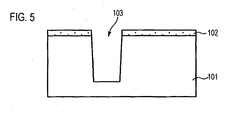
- Figs. 5 to 6D are schematic cross-sectional views showing a method of manufacturing a semiconductor device according to this embodiment.
- the trench 103 of 1 to 5 ⁇ m in depth is formed on a surface of the silicon substrate 101, after which the mask oxide layer 102 is removed.
- a silicon oxide layer is formed as the dielectric layer 104 in a thickness of 100 to 800 nm over an upper surface of the silicon substrate 101 and an inner wall of the trench 103, for example by a thermal oxidation process. Then a silicon oxide layer 120 is formed in a thickness of 150 to 1500 nm on the dielectric layer 104 for example by a CVD process, so that the trench 103 is filled with the silicon oxide layer 120,to thereby constitute a trench isolation region 121.
- a wet etching is performed so as to remove the silicon oxide layer 120 located on the upper surface of the silicon substrate 101 and the dielectric layer 104.
- an upper face of the silicon oxide layer 120 and dielectric layer 104 in the trench isolation region 121 becomes lower than the upper surface of the silicon substrate 101 because of an over etching, thereby forming a gap C.
- the gate insulating layer 106 When the gate insulating layer 106 is formed in a thickness of 3 to 30 nm, the gap C formed between the trench isolation region 121 and the silicon substrate 101 is reproduced in a shape of the gate insulating layer 106. Then after forming an impurity-diffused polycrystalline silicon layer 122 in a thickness of 100 to 600 nm so as to contact an upper surface of the gate insulating layer 106, an isolation region pattern 123 and the gate electrode pattern 114 are formed by a known lithography technique utilizing a resist (Fig. 6C). Here, as shown in Fig. 6C, the isolation region pattern 123 is located on the trench isolation region 121.
- an anisotropic etching is performed on the resist to remove a portion of the impurity-diffused polycrystalline silicon layer 122 exposing a surface thereof, after which the resist is removed, such that the gate electrode 108 and the trench shield 124 are formed (Fig. 6D).
- a portion of the gate insulating layer 106 that is in contact with the dielectric layer 104 in the trench isolation region 121 is covered with the trench shield 124.
- Such constitution prevents the impurity-diffused polycrystalline silicon layer 122 on the dielectric layer 104 from being peeled off to turn into a waste. Accordingly, the similar advantage as the first embodiment can be attained. Also, since the trench isolation region 121 is intended for element isolation, the impurity-diffused polycrystalline silicon layer 122 constituting the trench shield 124 provided on the trench isolation region 121 is electrically insulated from the surrounding circuit elements, and is therefore inhibited from causing undesired influence to a characteristic of the semiconductor device.
- the silicon oxide layer used to fill the trench 103 is somewhat inferior to the polycrystalline silicon layer in filling performance, however offers better insulation between layers. Therefore sufficient insulation is secured even in a finer isolation trench, which leads to further micronization of the semiconductor device.
- the silicon oxide layer 120 and the gate electrode 104 in the trench 103 are of the same material, the etching on these two layers is performed at a same rate, therefore a gap is not produced between the silicon oxide layer 120 and the dielectric layer 104. Also, while a thermal oxidation process is employed to form the silicon oxide layer to serve as the dielectric 104, a CVD process may also be employed.
- the trench shield 115 as well as trench shield 124 cover a portion of the gate insulating layer 106 that is in contact with the CVD layer filled in the trench isolation region 113 and the trench isolation region 121, respectively.
- Such constitution prevents emergence of an etching residue of the impurity-diffused polycrystalline silicon layer 107 on a portion of the gate insulating layer 106 on the filling polycrystalline silicon layer 105.
- a silicon oxide layer is employed to constitute the dielectric layer 104
- a silicon nitride layer may also be employed.
- a gap may be formed in the trench isolation region because of a difference of etching rate between the filling polycrystalline silicon layer 105 and the silicon oxide layer 120, however by carrying out the method of manufacturing according to the embodiments the foregoing advantages can equally be attained.
- impurity-diffused polycrystalline silicon layer 107 and the impurity-diffused polycrystalline silicon layer 122 are employed in the foregoing embodiments, other layers may be employed as long as it is a conductive layer.
- a metal layer such as a tungsten (W) layer may be employed, which may be formed by a sputtering process.
- another pattern for forming an interconnect may be employed as the pattern defined by a resist to cover the conductive layer, instead of the gate electrode pattern 114.
- the gate electrode pattern 114 may be omitted.
- filling polycrystalline silicon layer 105 is formed by a CVD process in the foregoing embodiment, other methods may be employed for this purpose.
- etching technique such as a dry etching may be employed for removing the dielectric layer 104.
- a method of manufacturing a semiconductor device that suppresses emergence of a waste in an isolation trench formation process is to be provided.
- the method comprises forming an isolation trench having a predetermined depth from a surface of a semiconductor substrate; forming a dielectric layer on the surface of the semiconductor substrate including the isolation trench; filling the isolation trench with a CVD layer; removing the dielectric layer except a portion in the isolation trench by an etching; sequentially forming an insulating layer and a conductive layer; forming a resist defining a pattern which covers via the conductive layer a portion of the insulating layer in contact with the dielectric layer; and performing an anisotropic etching on the resist to thereby remove a portion of the conductive layer exposing a surface thereof.
Landscapes
- Element Separation (AREA)
- Electrodes Of Semiconductors (AREA)
Abstract
Description
Claims (17)
- A semiconductor device, comprising:a semiconductor substrate;an isolation trench formed inside said semiconductor substrate;a first layer formed along an inner wall of said isolation trench so as to constitute a lining;a second layer formed in contact with an inner surface of said first layer so as to fill said isolation trench; anda conductive layer selectively formed on said isolation trench so as to cover said first layer and said second layer.
- The semiconductor device as recited in Claim 1, further comprising a gate electrode in a region different from said conductive layer, wherein said conductive layer and said gate electrode are formed in a same process.
- The semiconductor device as recited in Claim 2, further comprising an insulating layer over a first region where said conductive layer is provided and a second region where said gate electrode is provided, wherein said insulating layer insulates said first layer and said second layer in said first region, as well as said gate electrode and said semiconductor substrate in said second region.
- The semiconductor device as recited in Claim 1 to 3, wherein said second layer is a CVD layer.
- The semiconductor device as recited in Claim 4, wherein said CVD layer is a polycrystalline silicon layer.
- The semiconductor device as recited in Claim 4 to 5, wherein said CVD layer is constituted of a same material as said first layer.
- The semiconductor device as recited in Claim 1 to 6, wherein said first layer is a silicon oxide layer.
- A method of manufacturing a semiconductor device, comprising:forming an isolation trench having a predetermined depth from a surface of a semiconductor substrate;forming a dielectric layer on said surface of said semiconductor substrate including said isolation trench;filling said isolation trench with a CVD layer;removing said dielectric layer except a portion in said isolation trench by an etching;sequentially forming an insulating layer and a conductive layer;forming a resist defining a pattern which covers via said conductive layer a portion of said insulating layer in contact with said dielectric layer; andperforming an anisotropic etching on said resist to thereby remove a portion of said conductive layer exposing a surface thereof.
- The method as recited in Claim 8, further comprising:forming said insulating layer in contact with an upper surface of said dielectric layer, said CVD layer and said semiconductor substrate; andforming said conductive layer in contact with an upper surface of said insulating layer.
- The method as recited in Claim 8 to 9, wherein said resist is provided with a pattern for forming a gate electrode of a transistor.
- The method as recited in Claim 8 to 10, wherein said resist covers via said conductive layer a portion of said insulating layer in contact with said CVD layer.
- The method as recited in Claim 8 to 11, wherein said CVD layer is a polycrystalline silicon layer.
- The method as recited in Claim 8 to 12, wherein said CVD layer is constituted of a same material as said dielectric layer.
- The method as recited in Claim 8 to 13, wherein said dielectric layer is a silicon oxide layer.
- A method of manufacturing a semiconductor device, comprising:forming an isolation trench on an upper portion of a semiconductor substrate;forming a first layer in contact with an upper surface of said semiconductor substrate including an inner wall of said isolation trench;filling said isolation trench with a second layer;selectively removing said first layer except a portion in said isolation trench;forming an insulating layer so as to cover said first layer, said second layer and an upper surface of said semiconductor substrate;forming a conductive layer so as to cover an upper surface of said insulating layer;forming a resist defining a pattern which covers via said conductive layer a portion of said insulating layer in contact with said second layer and with said first layer; andselectively removing an exposed portion of said conductive layer and forming a gate electrode, and a conductive layer on top of said isolation trench.
- The method as recited in Claim 15, wherein said second layer is a CVD layer.
- The method as recited in claim 15, wherein a gap defined by side surfaces of said semiconductor substrate and said second layer and a top surface of said first layer in said trench is formed when said first layer is selectively removed; and said gap is filled with said insulating layer and said conductive layer.
Applications Claiming Priority (2)
| Application Number | Priority Date | Filing Date | Title |
|---|---|---|---|
| JP2003379835 | 2003-11-10 | ||
| JP2003379835A JP2005142481A (en) | 2003-11-10 | 2003-11-10 | Manufacturing method of semiconductor device |
Publications (2)
| Publication Number | Publication Date |
|---|---|
| EP1530233A2 true EP1530233A2 (en) | 2005-05-11 |
| EP1530233A3 EP1530233A3 (en) | 2006-03-22 |
Family
ID=34431385
Family Applications (1)
| Application Number | Title | Priority Date | Filing Date |
|---|---|---|---|
| EP04026578A Withdrawn EP1530233A3 (en) | 2003-11-10 | 2004-11-09 | Semiconductor device and method of manufacturing the same |
Country Status (4)
| Country | Link |
|---|---|
| US (2) | US7259073B2 (en) |
| EP (1) | EP1530233A3 (en) |
| JP (1) | JP2005142481A (en) |
| CN (1) | CN100397610C (en) |
Families Citing this family (9)
| Publication number | Priority date | Publication date | Assignee | Title |
|---|---|---|---|---|
| US20060078560A1 (en) * | 2003-06-23 | 2006-04-13 | Neopharm, Inc. | Method of inducing apoptosis and inhibiting cardiolipin synthesis |
| JP2009283488A (en) * | 2008-05-19 | 2009-12-03 | Toshiba Corp | Nonvolatile memory, and manufacturing method thereof |
| US8304329B2 (en) * | 2008-12-01 | 2012-11-06 | Maxpower Semiconductor, Inc. | Power device structures and methods |
| US9159808B2 (en) * | 2009-01-26 | 2015-10-13 | Taiwan Semiconductor Manufacturing Company, Ltd. | Selective etch-back process for semiconductor devices |
| CN104979196B (en) * | 2014-04-01 | 2018-09-25 | 中芯国际集成电路制造(上海)有限公司 | A kind of production method of channel-type semiconductor device structure |
| CN105118775B (en) * | 2015-08-18 | 2019-02-05 | 上海华虹宏力半导体制造有限公司 | Shielded gate transistor formation method |
| US10164982B1 (en) | 2017-11-28 | 2018-12-25 | Cyberark Software Ltd. | Actively identifying and neutralizing network hot spots |
| CN107993976B (en) * | 2017-12-07 | 2020-07-14 | 德淮半导体有限公司 | Semiconductor device and method of manufacturing the same |
| CN111354788B (en) * | 2020-03-24 | 2023-05-16 | 成都森未科技有限公司 | Deep trench insulated gate device and preparation method thereof |
Family Cites Families (38)
| Publication number | Priority date | Publication date | Assignee | Title |
|---|---|---|---|---|
| US4356211A (en) * | 1980-12-19 | 1982-10-26 | International Business Machines Corporation | Forming air-dielectric isolation regions in a monocrystalline silicon substrate by differential oxidation of polysilicon |
| US4926235A (en) * | 1986-10-13 | 1990-05-15 | Yoichi Tamaki | Semiconductor device |
| US4980747A (en) * | 1986-12-22 | 1990-12-25 | Texas Instruments Inc. | Deep trench isolation with surface contact to substrate |
| DE3752286T2 (en) * | 1986-12-22 | 2000-01-13 | Texas Instruments Inc., Dallas | Isolation formed in a deep trench with contact on the surface of the substrate |
| JPH0223630A (en) * | 1988-07-12 | 1990-01-25 | Seiko Epson Corp | Manufacturing method of semiconductor device |
| JPH0358470A (en) * | 1989-07-26 | 1991-03-13 | Takehide Shirato | Semiconductor device |
| US5433794A (en) * | 1992-12-10 | 1995-07-18 | Micron Technology, Inc. | Spacers used to form isolation trenches with improved corners |
| US5773871A (en) | 1993-06-24 | 1998-06-30 | Northern Telecom Limited | Integrated circuit structure and method of fabrication thereof |
| JPH0870101A (en) * | 1994-08-11 | 1996-03-12 | Northern Telecom Ltd | Integrated circuit capacitor structure and its preparation |
| JPH08288509A (en) * | 1995-04-14 | 1996-11-01 | Sony Corp | Semiconductor device and manufacturing method thereof |
| US5834811A (en) * | 1996-06-17 | 1998-11-10 | Taiwan Semiconductor Manufacturing Company, Ltd. | Salicide process for FETs |
| US5751040A (en) * | 1996-09-16 | 1998-05-12 | Taiwan Semiconductor Manufacturing Company Ltd. | Self-aligned source/drain mask ROM memory cell using trench etched channel |
| US5773821A (en) * | 1996-10-15 | 1998-06-30 | University Of Utah Research Foundation | Radiological surveying as a method for mapping fossilized bone sites |
| KR100268930B1 (en) * | 1996-11-12 | 2000-10-16 | 김영환 | Structure of thin-film transistor and manufacturing method thereof |
| US5763315A (en) * | 1997-01-28 | 1998-06-09 | International Business Machines Corporation | Shallow trench isolation with oxide-nitride/oxynitride liner |
| JP3519579B2 (en) * | 1997-09-09 | 2004-04-19 | 株式会社ルネサステクノロジ | Semiconductor device and manufacturing method thereof |
| US6960818B1 (en) * | 1997-12-30 | 2005-11-01 | Siemens Aktiengesellschaft | Recessed shallow trench isolation structure nitride liner and method for making same |
| US6165843A (en) * | 1998-03-20 | 2000-12-26 | Mosel Vitelic, Inc. | Covered slit isolation between integrated circuit devices |
| US6037018A (en) * | 1998-07-01 | 2000-03-14 | Taiwan Semiconductor Maufacturing Company | Shallow trench isolation filled by high density plasma chemical vapor deposition |
| JP2000077535A (en) * | 1998-09-02 | 2000-03-14 | Hitachi Ltd | Semiconductor device and manufacturing method thereof |
| US6180976B1 (en) * | 1999-02-02 | 2001-01-30 | Conexant Systems, Inc. | Thin-film capacitors and methods for forming the same |
| US6248641B1 (en) * | 1999-02-05 | 2001-06-19 | United Microelectronics Corp. | Method of fabricating shallow trench isolation |
| US6403445B1 (en) * | 1999-04-06 | 2002-06-11 | Advanced Micro Devices, Inc. | Enhanced trench isolation structure |
| JP2001135718A (en) * | 1999-11-08 | 2001-05-18 | Nec Corp | Manufacturing method of trench isolation structure |
| US6277697B1 (en) * | 1999-11-12 | 2001-08-21 | United Microelectronics Corp. | Method to reduce inverse-narrow-width effect |
| TW469635B (en) * | 2000-05-16 | 2001-12-21 | Nanya Technology Corp | Fabrication method of semiconductor memory cell transistor |
| JP2002237518A (en) * | 2001-02-08 | 2002-08-23 | Sony Corp | Semiconductor device and manufacturing method thereof |
| KR100407567B1 (en) * | 2001-04-10 | 2003-12-01 | 삼성전자주식회사 | Trench Isolation Process Without Dent |
| US6593192B2 (en) * | 2001-04-27 | 2003-07-15 | Micron Technology, Inc. | Method of forming a dual-gated semiconductor-on-insulator device |
| US6645795B2 (en) * | 2001-05-03 | 2003-11-11 | International Business Machines Corporation | Polysilicon doped transistor using silicon-on-insulator and double silicon-on-insulator |
| KR100389031B1 (en) * | 2001-06-19 | 2003-06-25 | 삼성전자주식회사 | Method of fabricating semiconductor device having trench isolation structure |
| US6566200B2 (en) * | 2001-07-03 | 2003-05-20 | Texas Instruments Incorporated | Flash memory array structure and method of forming |
| DE10164950B4 (en) * | 2001-09-07 | 2010-01-28 | Qimonda Ag | Method for producing a semiconductor integrated circuit |
| TW533536B (en) * | 2002-04-24 | 2003-05-21 | Nanya Technology Corp | Manufacturing method of shallow trench isolation |
| US6653203B1 (en) * | 2002-05-23 | 2003-11-25 | Taiwan Semiconductor Manufacturing Company | Thin sidewall multi-step HDP deposition method to achieve completely filled high aspect ratio trenches |
| US6750117B1 (en) * | 2002-12-23 | 2004-06-15 | Macronix International Co., Ltd. | Shallow trench isolation process |
| JP2004207564A (en) * | 2002-12-26 | 2004-07-22 | Fujitsu Ltd | Semiconductor device manufacturing method and semiconductor device |
| US6864152B1 (en) * | 2003-05-20 | 2005-03-08 | Lsi Logic Corporation | Fabrication of trenches with multiple depths on the same substrate |
-
2003
- 2003-11-10 JP JP2003379835A patent/JP2005142481A/en active Pending
-
2004
- 2004-11-09 EP EP04026578A patent/EP1530233A3/en not_active Withdrawn
- 2004-11-09 US US10/983,672 patent/US7259073B2/en not_active Expired - Fee Related
- 2004-11-10 CN CNB2004100883504A patent/CN100397610C/en not_active Expired - Fee Related
-
2006
- 2006-09-25 US US11/534,862 patent/US20070018276A1/en not_active Abandoned
Also Published As
| Publication number | Publication date |
|---|---|
| US20050101074A1 (en) | 2005-05-12 |
| CN1617321A (en) | 2005-05-18 |
| EP1530233A3 (en) | 2006-03-22 |
| US7259073B2 (en) | 2007-08-21 |
| JP2005142481A (en) | 2005-06-02 |
| CN100397610C (en) | 2008-06-25 |
| US20070018276A1 (en) | 2007-01-25 |
Similar Documents
| Publication | Publication Date | Title |
|---|---|---|
| US6852620B2 (en) | Semiconductor device with self-aligned junction contact hole and method of fabricating the same | |
| US5885883A (en) | Methods of forming trench-based isolation regions with reduced susceptibility to edge defects | |
| US6277709B1 (en) | Method of forming shallow trench isolation structure | |
| CN100385626C (en) | Method of forming gate structure for semiconductor device and semiconductor device | |
| US7148113B2 (en) | Semiconductor device and fabricating method thereof | |
| JPH08204014A (en) | Semiconductor device and manufacturing method thereof | |
| US6184127B1 (en) | Semiconductor processing method of forming a contact opening to a region adjacent a field isolation mass, and a semiconductor structure | |
| US11569369B2 (en) | Method for manufacturing a semiconductor device | |
| KR20050067466A (en) | Method of isolation in semiconductor device | |
| US7259073B2 (en) | Semiconductor device and method of manufacturing the same | |
| JP2001257325A (en) | Semiconductor memory device and method of manufacturing the same | |
| US20100052036A1 (en) | Memory device and manufacturing method thereof, and semiconductor device | |
| US20050142841A1 (en) | Method for forming metal pattern to reduce contact resistivity with interconnection contact | |
| US6303465B1 (en) | Method of forming low leakage current borderless contact | |
| CN100573870C (en) | Double shallow trench insulating semiconductor device and manufacturing method thereof | |
| US7691706B2 (en) | Method of fabricating a semiconductor device | |
| CN100394552C (en) | Method for forming contact window opening and method for manufacturing semiconductor element | |
| US6423612B1 (en) | Method of fabricating a shallow trench isolation structure with reduced topography | |
| JPH1012733A (en) | Semiconductor device and manufacturing method thereof | |
| JP2004165527A (en) | Semiconductor device and method of manufacturing semiconductor device | |
| US6420240B1 (en) | Method for reducing the step height of shallow trench isolation structures | |
| KR19990055791A (en) | Device Separation Method of Semiconductor Device | |
| TW202433605A (en) | Method of manufacturing semiconductor device | |
| CN117276081A (en) | Preparation method of shielded gate trench type MOSFET and shielded gate trench type MOSFET | |
| US7812415B2 (en) | Apparatus having gate structure and source/drain over semiconductor substrate |
Legal Events
| Date | Code | Title | Description |
|---|---|---|---|
| PUAI | Public reference made under article 153(3) epc to a published international application that has entered the european phase |
Free format text: ORIGINAL CODE: 0009012 |
|
| AK | Designated contracting states |
Kind code of ref document: A2 Designated state(s): AT BE BG CH CY CZ DE DK EE ES FI FR GB GR HU IE IS IT LI LU MC NL PL PT RO SE SI SK TR |
|
| AX | Request for extension of the european patent |
Extension state: AL HR LT LV MK YU |
|
| PUAL | Search report despatched |
Free format text: ORIGINAL CODE: 0009013 |
|
| AK | Designated contracting states |
Kind code of ref document: A3 Designated state(s): AT BE BG CH CY CZ DE DK EE ES FI FR GB GR HU IE IS IT LI LU MC NL PL PT RO SE SI SK TR |
|
| AX | Request for extension of the european patent |
Extension state: AL HR LT LV MK YU |
|
| 17P | Request for examination filed |
Effective date: 20060331 |
|
| AKX | Designation fees paid |
Designated state(s): DE FR IT |
|
| 17Q | First examination report despatched |
Effective date: 20070305 |
|
| RAP1 | Party data changed (applicant data changed or rights of an application transferred) |
Owner name: RENESAS ELECTRONICS CORPORATION |
|
| STAA | Information on the status of an ep patent application or granted ep patent |
Free format text: STATUS: THE APPLICATION IS DEEMED TO BE WITHDRAWN |
|
| 18D | Application deemed to be withdrawn |
Effective date: 20140603 |