EP1530132A2 - Arbitrierungsverfahren zum Zugriff auf ein verteiltes Betriebsmittel - Google Patents
Arbitrierungsverfahren zum Zugriff auf ein verteiltes Betriebsmittel Download PDFInfo
- Publication number
- EP1530132A2 EP1530132A2 EP04023275A EP04023275A EP1530132A2 EP 1530132 A2 EP1530132 A2 EP 1530132A2 EP 04023275 A EP04023275 A EP 04023275A EP 04023275 A EP04023275 A EP 04023275A EP 1530132 A2 EP1530132 A2 EP 1530132A2
- Authority
- EP
- European Patent Office
- Prior art keywords
- access
- count value
- circuit
- value
- penalty
- Prior art date
- Legal status (The legal status is an assumption and is not a legal conclusion. Google has not performed a legal analysis and makes no representation as to the accuracy of the status listed.)
- Withdrawn
Links
Images



Classifications
-
- G—PHYSICS
- G06—COMPUTING OR CALCULATING; COUNTING
- G06F—ELECTRIC DIGITAL DATA PROCESSING
- G06F13/00—Interconnection of, or transfer of information or other signals between, memories, input/output devices or central processing units
- G06F13/14—Handling requests for interconnection or transfer
- G06F13/36—Handling requests for interconnection or transfer for access to common bus or bus system
- G06F13/362—Handling requests for interconnection or transfer for access to common bus or bus system with centralised access control
- G06F13/364—Handling requests for interconnection or transfer for access to common bus or bus system with centralised access control using independent requests or grants, e.g. using separated request and grant lines
Definitions
- the present invention relates to a method and a device arbitration of access to a shared resource by several elements.
- Figure 1 schematically represents an example of arbitration device for accessing a shared resource.
- a group of master circuits M0, M1, ... Mi, ... Mn is connected to a shared resource via a circuit of multiplexing BMUX.
- the shared resource here includes a BSH bus and at least one peripheral circuit PPH connected to this bus, by example a memory of data and / or instructions forming a slave circuit.
- the group of master circuits includes by example of microprocessors, a DSP processor, co-processors, a DMA circuit (direct memory access circuit), a embedded video camera ...
- Such a mix of circuits sharing a common resource is common in integrated circuits for new generation mobile phones.
- the arbitration of the accesses to the memory PPH is ensured by a arbitration device ACT1 which receives access requests R0, R1, ... Ri, ... Rn provided by each of the master circuits and which provides a selection signal SEL on a control input of the BMUX circuit, by applying a determined arbitration rule.
- the Ri queries and access cycles to the shared resource are clocked by a clock signal common to the master circuits, which Synchronize access to the shared resource.
- DMA circuit can sometimes have need to access memory almost instantaneously (time to low latency), for example when transferring an important mass of data, and sometimes have a strong need for access to the memory for high speed transfers while being little sensitive to latency time.
- a video camera apart from his cyclic data rate corresponding to an image transfer, can sometimes require a high data rate.
- the present invention thus aims at a method and a device arbitration agreements that are highly flexible and are configurable according to the "profiles" of the elements sharing the shared resource, in terms of access needs.
- a first idea of the present invention is to provide for a first arbitration mechanism allowing ensure each element has minimal access to the resource shared at regular time intervals, according to a rule minimal sharing that can be configured at will.
- Another idea of the present invention is to provide a second arbitration mechanism to ensure that each element instant access to the shared resource without imposing a determined time interval between two accesses, according to a rule proportional partition that can be configured at will.
- the present invention provides a arbitration method of access to a resource that is shared by several electronic elements and which is accessible according to access cycles clocked by a clock signal, wherein each element wishing to access the shared resource issues an access request, a process in which: each element is seen assign a first count value and a first penalty, the first count value of each element is decremented, or incremented, in synchronization with the signal clock, the first count value of each element is incremented, or respectively decremented, by a value equal to the first penalty, whenever the item is selected for an access cycle, and when multiple elements wait simultaneously access the shared resource, an element is selected to access the resource if its first value of count is less than or equal to or greater than or equal to equal to a specified threshold, and if its first count value is less, or respectively greater than, the first count values of other items that issued a request access.
- an element is selected whatever its first count value, if it is the only one to request access to the shared resource.
- two elements capable of to be selected have the same first count value, the element to be selected is designated by applying a rule of predetermined selection.
- the access requests can several successive access cycles and, where element having issued an access request for several access cycles is selected, access to the shared resource is granted to the element during the number of access cycles requested, even if, after the first access cycle of the element, the item is no longer selectable by virtue of its first count value.
- the first count value an element is inhibited when the element is not querying during a given number of access cycles.
- each element is seen assign a second count value and a second penalty, the second count value of each element is incremented, decremented, of a value equal to the second penalty, each time the element is selected, and when multiple elements simultaneously waiting to access the shared resource, if no element is selectable by virtue of its first value count, the selected element is the one whose second count value is less, or respectively greater, the second count values of the other elements that issued an access request.
- the second count value an element is held at a specified value when the item does not issue an access request for a number of determined of access cycles.
- the second count value an item that did not issue an access request during a determined number of access cycles is kept at a value equal to the lowest second count value of the elements issuing access requests.
- the first count value each element is incremented, or decremented respectively, value equal to the first penalty, whenever the element is selected by virtue of its second value of counting, and vice versa the second count value of each element is also incremented, or respectively decremented, of a value equal to the second penalty, each once the item is selected by virtue of its first value count.
- the access requests can several successive access cycles and, where element having issued an access request for several access cycles is selected, access to the shared resource is granted to the element during the number of access cycles requested, even if, after the first access cycle of the element, the item is no longer selectable by virtue of its first and second count values.
- the method is applied to a device in which the shared resource is a bus of data connected to one or more peripheral circuits by through an access multiplexing circuit, the electronic elements being relatively master circuits peripheral circuits.
- the multiplexing circuit access provides control signals designating the circuit master selected at each access cycle, and the signals of control are used to identify count values to be decremented or incremented at each access to the bus of data.
- the present invention also relates to a device arbitration of access to a shared resource by several electronic elements, the shared resource being accessible according to access cycles clocked by a clock signal, each element that wants to access the shared resource that is to broadcast an access request, the device comprising first registers for memorizing, for each element, a first penalty assigned individually to each element, first counters to individually assign to each element a first count value, and to decrement, or increment, the first count value in synchronization with the clock signal, and increment, or respectively decrement, the first count value of a value equal to the first penalty, whenever the corresponding element is selected for an access cycle, and a first circuit of comparison to provide, when multiple elements are waiting simultaneously access the shared resource, a first selection signal designating an element whose first value count is less than or equal to or greater than equal to a specified threshold, and the first value of which count is less, or respectively greater, than first count values of other elements that have issued a access request.
- the device comprises means to select an item that is alone to request access to the shared resource, regardless of the first count value of the element.
- the first circuit of comparison is arranged to select one of these elements according to a predetermined selection rule.
- the device comprises a management circuit of the first meters to inhibit the first count value of an item that has not issued any access request during a determined number of access cycles.
- the device comprises in in addition to second registers for storing, for each element, a second penalty assigned individually to each element, second counters to assign individually to each element a second count value, and to increment, or decrement, the second count value of a value equal to the second penalty, whenever the corresponding element is selected for an access cycle, and a second circuit of comparison to provide, when multiple elements are waiting simultaneously access the shared resource, a second signal of selection designating an element whose second value of count is less, or respectively greater, than second count values of the other elements that have issued a access request.
- the first and second signals selection are applied to a multiplexer circuit whose output provides a general selection signal equal to the second selection signal when the first comparison circuit find no element to select, if not equal to the first signal Selection.
- the first count value each element is incremented, or decremented respectively, value equal to the first penalty, whenever the element is selected by virtue of its second value of counting, and vice versa the second count value of each element is incremented, or respectively decremented, of a value equal to the second penalty each time the element is selected by virtue of its first value of counting.
- the device comprises a second meter management circuit to maintain the second count value of an item at a specified value when the item does not issue an access request for a number of determined of access cycles.
- the management circuit of the second counters maintains the second count value of a element that did not issue an access request for a number of determined from access cycles, to a value equal to the lowest second count value of elements emitting requests access.
- the device comprises a Burst access request management circuit which is arranged to maintain selection of a selected item, even if, after the first access cycle granted to the element, this element is not selectable by virtue of its first or second count value.
- the device comprises a access multiplex circuit to connect to the resource shared, at each access cycle, a selected element.
- the multiplexing circuit access provides control signals designating the circuit master selected at each access cycle, the signals of control being applied to the meters as loading, for loading the first or the second penalty.
- the shared resource is a bus connected to one or more peripheral circuits, the elements electronic circuits being master circuits relative to peripheral circuits.
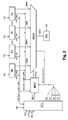
- a PPH resource is shared by elements Mi (M0, M1, ... Mn).
- the resource includes a BSH bus connected to a peripheral circuit PPH.
- Mi elements are master circuits relative to the peripheral circuit.
- the circuit peripheral is for example a memory accessible in readind, writing.
- bus BSH is the shared resource. In effect if multiple devices are connected to the bus, each master circuit must first access the bus to access one of the peripherals.
- the bus is, conceptually, the first resource to which the master circuits must to access.
- Access to the bus is controlled by an arbitration system comprising a BMUX multiplexing circuit, a management circuit BMCT burst access ("Burst Management Circuit"), and a ACT2 arbitration circuit according to the invention.
- the BMUX multiplex circuit has n + 1 inputs connected to the Mi master circuits and an output connected to the bus BSH.
- Each master circuit Mi is connected to a circuit input BMUX via a BMi bus (BM0, BM1, ... BMn).
- the buses BMi and the bus BSH include for example N data son and M parallel address wires, and possibly various other wires necessary for the exchange of data between the master circuits and the peripheral circuit. The data is therefore transferred between the master circuits and the circuit peripheral by words of N + M bits in parallel, via the circuit BMUX.
- Each master circuit Mi provides a request signal RQi (RQ1 to RQn) encoded on a bit, and a burst signal BSi (BS0 to BSn) encoded on several bits.
- the request signal RQi is carried at 1 when the master circuit Mi wishes to access the bus, while that the burst signal BSi ("burst" signal) indicates the number Bi words that the master circuit wishes, if any, to emit one after another.
- the signal BSi is for example encoded on 4 bits and lies between 0 and 15.
- the circuit ACT2 provides a signal of selection SEL1 which is applied on an input of the circuit BMCT. This provides a selection signal SEL2 which is applied on a control input of the BMUX circuit.
- the BMUX circuit connects to bus BSH the master circuit Mi which is designated by the signal of SEL2 selection.
- the circuit ACT2 receives the RQi request signals provided by the Mi master circuits, while the BMCT circuit receives at both the request signals RQi and the burst signals BSi.
- the BMCT circuit is transparent vis-à-vis the ACT2 circuit.
- the ACT2 circuit provides the SEL1 signal selecting the master circuit and the signal SEL2 copies the signal SEL1.
- the circuit BMCT When a master circuit requests access to the BSH bus for several access cycles (BSi ⁇ 0), and when this circuit master is selected by the circuit ACT2, the circuit BMCT is transparent for the first access cycle and then maintains the signal SEL2 to the initial value of the signal SEL1 until Burst access is terminated even if the SEL1 signal has meanwhile changed value.
- the BMUX circuit also provides Gi control signals (G0 to Gn) indicating, at each access cycle, what is the circuit Mi master to which access to the bus is granted. For example, the signal G1 is at 1 when the master circuit M1 accesses the bus, while the other signals G0, G2, ... Gn are at 0. These signals are automatically managed by the BMUX circuit according to the selection signal SEL2 received on its control input.
- a bus access cycle extends on n clock cycles, for example two clock cycles.
- the BMUX and BMCT circuits are in themselves elements classics found in standard components, for example in the circuit marketed by the company ARM® under the BUS-MATRIX reference.
- the selection signal SEL1 is provided by an arbitration circuit classic built-in component, which offers only a fixed priority arbitration.
- This classic referee circuit is replaced by the circuit ACT2 according to the invention.
- Such a replacement consists of a disabling the conventional arbitration circuit, and a transplant ACT2 circuit on a bypass input of the circuit classic arbitration.
- the "bandwidth" BW of the resource shared is the maximum number of bus access per unit of time, for example per second.
- This bandwidth BW is distributed to the master circuits according to two mechanisms arbitration, respectively called “arbitration in minimum access "and” proportional access arbitration ", allowing to show a "minimum bandwidth” MBW and a “proportional bandwidth” PBW.
- the minimum bandwidth MBW represents a minimal number of access per unit of time which is guaranteed to all master circuits. This minimal bandwidth represents everything or part of the total bandwidth BW of the bus, and is distributed between each master circuit according to the "profile" of each, that is, his need to access the bus at intervals of regular times. This defines a minimum bandwidth individual MBWi for each master circuit Mi, which represents the number of accesses per unit of time that is guaranteed at each master circuit, the minimum bandwidth MBWi allocated to each master circuit being a fraction of the bandwidth global minimum MBW.
- each master circuit attribute to each master circuit a minimum access count value MCVi, and a penalty in minimal access MPi.
- the MCVi minimum access count value of each master circuit Mi is decremented by a number D at each clock cycle, in an equal manner for each master circuit, and is incremented by a value equal to the MPi penalty when a master circuit obtains a cycle of access to the bus.
- arbitration is ensured by applying a conventional arbitration rule of conventional type, for example a fixed priority or priority arbitration rule rotating.
- the relative minimum bandwidth MBW% granted to all the master circuits is thus equal to:
- This overall minimum bandwidth expressed in value relative should preferably be less than 1 so that it remains bandwidth to be distributed, for example by means of the proportional access arbitration mechanism described below.
- bus access can also be fully managed by the arbitration mechanism with minimal access.
- D will be considered as always equal to 1, each minimum access count value being decremented by 1 at each clock cycle.
- the two master circuits thus receive a total bandwidth of at least 12 MA / s. There remains 23 MA / s of bandwidth to be distributed as a proportional bandwidth, as described below.
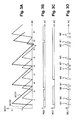
- FIGS. 3A to 3D illustrate an arbitration sequence in minimal access, the horizontal axis of the figures representing AC access cycles.
- Figure 3A shows the values of counting MCV0, MCV1 master circuits M0, M1.
- Figure 3B represents the request signal RQ0 supplied by the circuit M0 and
- FIG. 3C represents the request signal RQ1 provided by the M1 circuit these signals being set to 1 when a bus access is request.
- Figure 3D shows the cycles during which the circuits M0, M1 have access to the bus (signal SEL1).
- the minimum access penalty assigned to the M0 circuit is equal to 6 and the penalty in minimal access assigned to the M1 circuit is equal to 12.
- the high THR threshold priority is here equal to 0, as proposed above.
- the circuit M0 With each access to the bus, the circuit M0 sees its value of counting MCV0 incremented by 6, and the circuit M1 sees its value counting of MCV1 incremented by 12, each circuit obtaining principle access to the bus when its count value reaches the threshold 0. However, in cycle 35 the count value MCV0 of M0 circuit continues to be decremented towards the values negative. Indeed, it is assumed here that access to the bus can not be granted to the M0 circuit because other master circuits, having counting values lower than that of the circuit M0, are priority (these other count values are not shown in the figure for the sake of simplicity). So, the circuit M0 must wait for cycle 37 to access the bus.
- the count value MCV0 is incremented by 6 but present, after incrementation, a value of less than 6, having was incremented from a negative value.
- the circuit M0 will catch up in subsequent cycles, since the threshold 0 will be reached faster.
- the counting value MCV1 of the circuit M1 reaches the threshold 0 but access can not be granted, since it is primarily granted to the circuit M0, the count value of which is low.
- the count value MCV1 therefore also tends towards a negative value, up to cycle 38 where access is granted to M1 circuit (see also Fig. 3D).
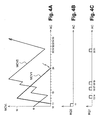
- FIGS. 4A to 4C illustrate such a case of figure.
- FIG. 4A represents the count values MCV0, MCV1 of the master circuits M0, M1
- FIG. 4B represents the request signal RQ0 of the circuit M0
- FIG. 4C the signal of request RQ1 of the circuit M1.
- Minimum access penalties for circuits M0, M1 are always equal to 6 and 12, respectively.
- BSO burst signal
- a mechanism for inhibiting the count values is preference provided, when the master circuits do not emit request during a given number of access cycles.
- This mechanism of inhibition is for example to force to 0 the counting value of the inactive master circuit. So, on the example of FIG. 4A, the count value MCV1 is kept at 0 when it reaches 0 because the M1 circuit does not have Issued for more than 10 access cycles. In practice, he however, it is better to choose an inactivity threshold greater than the time elapsing between the instant of application of the penalty and the moment or the threshold of high priority is reached (ie the duration of the "sawtooth" in Figure 4A). This amounts to waiting until the count value has reached negative values before inhibiting it back to 0.
- the proportional bandwidth PBW is the part of the total bandwidth of the shared resource which is distributed to the master circuits through the mechanism proportional access arbitration system according to the invention.
- this bandwidth proportional represents all or part of the bandwidth total BW of the shared resource, and is split between each master circuit according to the "profile" of each, that is to say here according to his instant need to access the bus.
- This band individual proportional pass PBWi is allocated by means of a proportional access count value PCVi specific to each master track Mi, and a penalty in access proportional PPi, also specific to each master circuit Mi.
- the count value PCVi of each master circuit is incremented by a value equal to the PPi penalty whenever the master circuit obtains access to the bus for an access cycle.
- access is granted to the one whose value is counting is the lowest.
- the arbitration is performed according to a predetermined arbitration rule, for example by fixed or rotating priority.
- Every master circuit Mi has, on average, the possibility to access the bus in a proportion defined by its PPi proportional access penalty.
- FIGS. 5A to 5E illustrate an example of arbitration in proportional access, the horizontal axis of the figures representing AC access cycles.
- Figure 5A shows the values of counting PCV0, PCV1, PCV2 master circuits M0, M1, M2.
- the FIGS. 5B, 5C, 5D respectively represent the requests access RQ0, RQ1, RQ2 provided by the master circuits.
- the FIG. 5E represents the cycles during which the circuits M0, M1, M2 have access to the bus (signal SEL1).
- the penalty PP0 assigned to the circuit M0 is equal to 2
- the penalty PP1 the circuit M1 is equal to 3
- the penalty PP2 allocated to the circuit M2 is equal to 6.
- the M0 circuit enjoys the greatest number of accesses because it has a relative proportional bandwidth of 50% (see relation 12 above).
- the M2 circuit benefits of the lowest proportional bandwidth and has to wait between cycles 4 and 9 that the circuits M0, M1 have several bus accesses so that its count value becomes lower than those of circuits M0, M1.
- the access arbitration mechanism Proportional only occurs when there is a collision between requests. If one of the master circuits is the only one to request access to the bus, this access is granted even if its count value in proportional access is not the weakest. So, a value proportional access counting is not taken into account in the comparison of the count values, when the master circuit correspondent did not issue an access request.
- the proportional access count value PCVi of each master circuit is preferably incremented by the proportional access penalty PPi whenever the circuit master gets access to the bus for an access cycle, that this access under the access arbitration mechanism minimum or the proportional access arbitration mechanism.
- the minimum access count value MCVi of each master circuit is preferably incremented by the minimum access penalty MPi each time the master circuit gets access to the bus for an access cycle, whether this access is granted under the minimum access arbitration mechanism or the proportional access arbitration mechanism.
- circuits M0, M1, M2 are active and constantly seek access to the bus.
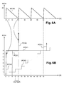
- Figure 6A shows the access count value MCV0 minimum of the M0 circuit, access count values minimum of the other circuits being inhibited because of the value zero assigned to their minimum access penalties.
- Figure 6B represents the proportional access count values PCV0, PCV1, PCV2 circuits M0, M1, M2.
- the horizontal axis of the figures 6A, 6B is graduated here in CK clock cycles.
- circuits M0, M1, M2 get 10%, 10% and 80% of access arbitration bandwidth proportional, ie respectively 2 MA / s, 2 MA / s, 16 MA / s.
- the 2 MA / s attributed to the M0 circuit under proportional access arbitration are less than 5 MA / s awarded under the minimum access arbitration. So, the M0 circuit is sufficiently served under the minimal access (5 MA / s) and access bandwidth proportional is not used. It thus appears in FIG. 6B that the count value in proportional access PCV0 of the circuit M0 increases rapidly because it is incremented each time access is granted to the M0 circuit under arbitration minimum access (ie every 20 clock cycles, when the counting value MCV0 reaches the threshold 0, see figure 6A). Thus, the circuit M0 never gets access to the resource at title of the proportional access arbitration because its value of PCV0 count remains higher than those of circuits M1, M2.
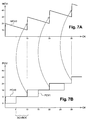
- Figure 7A shows the access count value MCV0 minimal circuit M0.
- Figure 7B shows the values proportional access counting PCV0, PCV1 of the M0 circuits, M1.
- the horizontal axis of the figures is as previously graduated in clock cycles.
- Circuits M0, M1 having the same penalty in access proportional, they each receive 50% of the bandwidth, that is 10 MA / s each. However, the 10 MA / s allocated to the M0 circuit at proportional access arbitration are superior to the 5 MA / s awarded under the minimum access arbitration. So the M0 circuit is sufficiently served under the proportional access and its minimal access bandwidth is not used. It thus appears in FIG. 7A that the value of MCV0 minimum access count of the M0 circuit increases rapidly for each access granted under the access arbitration proportional, when in FIG. 7B the counting value PCV0 is lower than that of the circuit M1. Thus, the M0 circuit never gets access to the resource under arbitration in minimal access, because its counting value MCV0 always remains greater than 0. When the count values PCV0, PCV1 are equal, the priority is arbitrarily given to the circuit M0.
- Penalties with minimal access and proportional access are chosen so that the distribution of the bandwidth Theoretical is consistent with the values given above.
- Column 1 of the table (“Case A”) describes the result of arbitration when circuits M1, M2, M3, M4 are active and constantly request access to the shared resource.
- the column 2 of the table (“case B”) describes the result of the arbitration when the circuit M1, for example a video camera, is stopped (OFF), while the M2, M3, M4 circuits are active and constantly request access to the shared resource.
- the column 3 of the table (“case C”) describes the result of the arbitration when the circuits M3, M4, for example microprocessors or co-processors, are stopped (OFF), while the circuits M1, M2 are active and constantly seeking access to the shared resource.
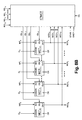
- FIG. 8A represents an exemplary embodiment of the circuit ACT2.
- the circuit ACT2 comprises registers MREGi (MREG0, MREG1, ... MREGn) to record MPi mode penalties minimum access arbitration rules MPi, and PREGi registers (PREG0, PREG1, ... PREGn) to record the PPi penalties of the mode proportional access arbitration.
- Each register MREGi, PREGi is connected to a DIN input of the ACT2 circuit, on which the MPi penalties, PPi to load in the registers are applied.
- the selection of each register for the loading of a penalty is provided by a RADEC address decoder circuit. This last receives on a first entry a RAD address designating the register to be selected and on a second input a signal of loading LOADR, and applies the LOADR signal to the designated register by the RAD address.
- the circuit ACT2 also includes MCTi counters (MCT0, MCT1 ... MCTn) containing the minimum access count values MCVi, and PCTi counters (PCT0, PCT1 ... PCTn) containing the proportional access count values PCVi.
- MCTi counters MCT0, MCT1 ... MCTn
- PCTi counters PCT0, PCT1 ... PCTn
- Each counter MCTi comprises an adding input IN1, a LOADIN loading input, and an OUT output.
- the entrance adding machine IN1 is connected to the output of a register MREGi of corresponding rank, to receive the minimum access penalty MPi corresponding.
- the LOADIN input receives a control signal Gi of corresponding rank, provided by the multiplexing circuit BMUX, see figure 2.
- each PCTi counter includes an input adding machine IN1, a loading input LOADIN, and an output OUT.
- the adding input IN1 is connected to the output of a register PREGi of corresponding rank, to receive the penalty corresponding proportional access PPi.
- the LOADIN entry receives a control signal Gi of corresponding rank.
- the minimum access count values MCVi provided by the MCTi counters are applied on inputs of a circuit for the MCOMP comparison, through logic gates 4 of type AND.
- Each AND gate receives on a second input the signal of request RQi issued by the master circuit Mi rank corresponding, and on a third input an MNOPi signal (MNOP0, MNOP1, ... MNOPn) provided by the register MREGi of rank corresponding.
- MNOP0, MNOP1, ... MNOPn MNOP0, MNOP1, ... MNOPn
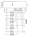
- the PCVi proportional access metering values provided by the PCTi counters are applied on inputs of a PCOMP comparison circuit, via gates logical 5 of type ET.
- Each AND gate receives on a second input the request signal RQi issued by the master circuit Mi of corresponding rank, and on a third input a PNOPi signal (PNOPO, PNOP1, ... PNOPn) provided by the rank PREGi register corresponding.
- PNOPO, PNOP1, ... PNOPn PNOPi signal
- the AND gate corresponding is not busy and the count value PCVi is not applied to the PCOMP comparison circuit.
- a register PREGi receives a penalty PPi of null value
- the corresponding PNOPi signal goes to 0, the AND gate corresponding is not busy and the count value PCVi is not applied to the PCOMP comparison circuit.
- the MCOMP circuit provides an MSEL selection signal in minimal access and NOSEL signal of non-selection, and receives on an auxiliary input a binary coded STHR signal whose value represents the high priority THR threshold described above.
- the signal MSEL designates the rank of the input of the MCOMP circuit on which a count value is applied MCVi which is below the THR threshold and which is the lowest of all the count values received by the other inputs of the MCOMP circuit.
- the rank of the input designated by the MSEL signal being the rank of the corresponding master track Mi, the signal MSEL designates the master circuit to be selected under the access minimal.
- the MCVi count values which are inhibited by the AND gates in the absence of a request access are not taken into account in this selection.
- the MSEL signal is brought to a value predetermined and the NOSEL signal is set to 1.
- the PCOMP circuit provides a selection PSEL signal in proportional access.
- the PSEL signal designates the rank of the PCOMP circuit input on which the PCVi count value which is higher than the other values of counting received by the other PCOMP circuit inputs.
- the row of the input indicated by the signal PSEL being the rank of the circuit corresponding Mi teacher, the signal PSEL designates the master circuit to be selected under proportional access.
- the MSEL, PSEL signals are applied to two inputs of one MUX1 multiplexer whose output provides the selection signal SEL1.
- the multiplexer MUX1 receives on a control input the NOSEL signal, and outputs the MSEL signal when NOSEL is at 0, or the PSEL signal when the NOSEL signal is at 1.
- the choice of the size of the counters depends on the penalty maximum that can be attributed to the circuits masters, and the maximum number of burst accesses possible. If one aims for a precision of 3% in the distribution of the bandwidth minimum and proportional bandwidth, the penalties in minimum and proportional access must range from 0 to 31 per no 1 (ie 0, 1, 2 ... 31). In this case, if the maximum number burst is 16, the meters must be able to accept count values up to 16 * 32 or 512 by value positive. Since the MCTi minimum access counters must also be able to count negative values, chooses counters 10 bits to complement by 2 can count up to -512 and +511. Proportional access meters do not receiving no negative value, one can choose meters 10 bits without complement by 2, ranging from 0 to 1023, even from higher range meters if you want to be able to program significant differences between proportional access penalties.
- the ACT2 arbitration circuit also includes a circuit CTMCT for MCTi and PCTi counters management.
- Each minimum access meter MCTi includes, in addition to the inputs already described, an IDL entry to place it in a state of inhibiting the count value MCVi.
- the circuit CIMCT monitors the request signals RQi issued by the master circuits, as well as the outputs of the meters MCTi, and receives on auxiliary inputs an encoded SNCY signal binary representing an NCY threshold, as well as the coded STHR signal binary representing the high priority THR threshold.
- the circuit CIMCT counts the number of clock cycles occurring between each query, and compare it to the NCY threshold.
- the CIMCT circuit monitors then the output of the corresponding MCTi counter and waits for the count value MCVi is equal to THR threshold.
- the circuit CIMCT applies an IDLi inhibition signal to the IDL input of the counter Corresponding MCTi. The count value is thus blocked on the threshold THR, until the circuit master concerned re-issue access requests.
- Each PCTi counter includes, in addition to entries already described, a non-adding input SET and a LOADSET input.
- the SET input is used to load the counter with a value of count determined by overwriting the current count value. AT this effect, a load signal SETi shall be applied on the LOADSET input of the meter.
- the circuit CTMCT monitors the request signals RQi issued by the master circuits, as well as the outputs of the meters ITCP.
- the CTMCT circuit counts the number of clock cycles intervening between each query, and compares it to the NCY threshold described above. When an RQi request signal has not passed at 1 since a number of clock cycles greater than or equal to NCY, the CTMCT circuit reads the outputs of all PCTi counters and search the lowest PCVi count value, which one will designate LVAL.
- the CIMCT circuit then charges this weaker count value in the PCTi counter of the master circuit which no longer issue an access request, applying the value LVAL on the counter's SET input and applying a load signal SETi on the LOADSET input of the meter.
- the CTMCT circuit also manages the counting window of the PCTi counters. In fact, proportional access count values are constantly incremented by proportional access penalties and are never decremented. In order to avoid the saturation of the counters, the counting values are reduced by a value equal to the Half Counter Range (HCR), for example 512, when they are all in half counter upper counter window, for example between 512 and 1024.
- HCR Half Counter Range
- the count values MCVi are incremented to the rhythm of the clock signal and are decremented with minimum access penalties.
- the high priority threshold is not a lower threshold but a threshold to be attained in order to benefit from access to common resource.
- the PCVi count values can be decremented with the penalties in proportional access to the instead of being incremented.
- the master circuit priority for proportional access is the one whose count value is the highest.
- a alternative embodiment includes assigning identical penalties and to assign decrements "Di" (D0, D1, ... Dn) variables, which leads to the same technical effect since this is the ratio between the value of a penalty and the decrement that determines the number of clock cycles between two Access permissions for minimum access (the base time allocated to each master circuit).
- the two arbitration mechanisms according to the invention are independent of one another and can be each independently of the other or in combination.
- arbitration can be fully managed by the mechanism with minimal access. It is also possible to entrust to a conventional arbitration process (fixed priority, Round Robin ...) the bandwidth left free through minimum access arbitration. This may include default arbitration method provided in the standard circuit BMUX described above.
- the combination of the two mechanisms arbitration is preferably interactive, which means that the two count values of the same master circuit are incremented with each access to the shared resource, that this access be granted under the minimum access arbitration or proportional access arbitration.
- the combination of the two arbitration mechanisms also be implemented without interactivity between the mechanisms arbitration, while giving priority to access arbitration minimal.
- the arbitration method according to the invention is susceptible to various other applications.
- the implementation of the method according to the invention can take various forms and the process can be applied to various elements.
- the means of access to the shared resource can various forms other than that of a circuit of multiplexing. It can be for example a generator of authorization signals which, starting from the current value of the selection signal SEL allows such an element to use the resource and prohibits others from using the resource.
Landscapes
- Engineering & Computer Science (AREA)
- Theoretical Computer Science (AREA)
- Physics & Mathematics (AREA)
- General Engineering & Computer Science (AREA)
- General Physics & Mathematics (AREA)
- Bus Control (AREA)
Applications Claiming Priority (2)
| Application Number | Priority Date | Filing Date | Title |
|---|---|---|---|
| FR0311973 | 2003-10-14 | ||
| FR0311973A FR2860896A1 (fr) | 2003-10-14 | 2003-10-14 | Procede d'arbitrage de l'acces a une ressource partagee |
Publications (2)
| Publication Number | Publication Date |
|---|---|
| EP1530132A2 true EP1530132A2 (de) | 2005-05-11 |
| EP1530132A3 EP1530132A3 (de) | 2007-12-26 |
Family
ID=34355448
Family Applications (1)
| Application Number | Title | Priority Date | Filing Date |
|---|---|---|---|
| EP04023275A Withdrawn EP1530132A3 (de) | 2003-10-14 | 2004-09-30 | Arbitrierungsverfahren zum Zugriff auf ein verteiltes Betriebsmittel |
Country Status (3)
| Country | Link |
|---|---|
| US (1) | US7404024B2 (de) |
| EP (1) | EP1530132A3 (de) |
| FR (1) | FR2860896A1 (de) |
Families Citing this family (17)
| Publication number | Priority date | Publication date | Assignee | Title |
|---|---|---|---|---|
| JP4480427B2 (ja) * | 2004-03-12 | 2010-06-16 | パナソニック株式会社 | リソース管理装置 |
| JP4436367B2 (ja) * | 2004-06-24 | 2010-03-24 | パナソニック株式会社 | 低バンド幅で局所集中アクセスを保証する調停装置、調停方法、及び調停装置を含む動画処理装置 |
| JP4907166B2 (ja) * | 2005-01-12 | 2012-03-28 | パナソニック株式会社 | リソース管理装置 |
| WO2006080371A2 (ja) * | 2005-01-31 | 2006-08-03 | Matsushita Electric Industrial Co Ltd | アクセス調停装置、および調停可能条件検証装置 |
| JP2007018280A (ja) * | 2005-07-07 | 2007-01-25 | Oki Electric Ind Co Ltd | バスシステムの制御方法及び制御回路 |
| JP2008045507A (ja) * | 2006-08-18 | 2008-02-28 | Nikki Co Ltd | 電磁燃料ポンプ |
| JP2008071036A (ja) * | 2006-09-13 | 2008-03-27 | Matsushita Electric Ind Co Ltd | リソース管理装置 |
| US7512723B2 (en) * | 2006-12-29 | 2009-03-31 | Freescale Semiconductor, Inc. | Queued interface devices, multi-core peripheral systems, and methods for sharing a peripheral in a multi-core system |
| JPWO2009139109A1 (ja) * | 2008-05-13 | 2011-09-15 | パナソニック株式会社 | メモリ制御装置、およびこれを備えた情報処理装置 |
| US20100162256A1 (en) * | 2008-12-18 | 2010-06-24 | Alexander Branover | Optimization of application power consumption and performance in an integrated system on a chip |
| WO2012145416A1 (en) * | 2011-04-20 | 2012-10-26 | Marvell World Trade Ltd. | Variable length arbitration |
| US8862909B2 (en) | 2011-12-02 | 2014-10-14 | Advanced Micro Devices, Inc. | System and method for determining a power estimate for an I/O controller based on monitored activity levels and adjusting power limit of processing units by comparing the power estimate with an assigned power limit for the I/O controller |
| US8924758B2 (en) | 2011-12-13 | 2014-12-30 | Advanced Micro Devices, Inc. | Method for SOC performance and power optimization |
| US10929551B2 (en) * | 2013-03-13 | 2021-02-23 | Comcast Cable Communications, Llc | Methods and systems for managing data assets |
| US9704355B2 (en) * | 2014-10-29 | 2017-07-11 | Clover Network, Inc. | Secure point of sale terminal and associated methods |
| US9747215B2 (en) * | 2015-12-14 | 2017-08-29 | Via Alliance Semiconductor Co., Ltd. | Stride reference prefetcher |
| CN106776371B (zh) * | 2015-12-14 | 2019-11-26 | 上海兆芯集成电路有限公司 | 跨距参考预取器、处理器和将数据预取到处理器的方法 |
Family Cites Families (23)
| Publication number | Priority date | Publication date | Assignee | Title |
|---|---|---|---|---|
| US757285A (en) | 1903-10-21 | 1904-04-12 | Paul Duchemin | Support for slates or tiles on roofs. |
| US1593408A (en) | 1926-02-24 | 1926-07-20 | Harry H Honigbaum | Retainer for composition roofing |
| US3738076A (en) | 1971-09-07 | 1973-06-12 | G Kessler | Nailing clip for plastic siding |
| US4642758A (en) * | 1984-07-16 | 1987-02-10 | At&T Bell Laboratories | File transfer scheduling arrangement |
| US5010476A (en) * | 1986-06-20 | 1991-04-23 | International Business Machines Corporation | Time multiplexed system for tightly coupling pipelined processors to separate shared instruction and data storage units |
| US5297383A (en) | 1989-03-13 | 1994-03-29 | Binda Nominees Pty Ltd. | File clip, apparatus and installation method |
| US5150555A (en) | 1991-07-12 | 1992-09-29 | Wood Larry A | Siding clip |
| US5339608A (en) | 1991-12-13 | 1994-08-23 | C & H Enterprises | Mounting clip for vinyl siding |
| US5471588A (en) * | 1992-11-25 | 1995-11-28 | Zilog, Inc. | Technique and circuit for providing two or more processors with time multiplexed access to a shared system resource |
| US5392033A (en) * | 1993-01-05 | 1995-02-21 | International Business Machines Corporation | Priority generator for providing controllable guaranteed fairness in accessing a shared bus |
| US5392579A (en) | 1993-09-13 | 1995-02-28 | Champagne; Charles A. | Lipless clip for vinyl siding and method |
| US5564245A (en) | 1994-05-18 | 1996-10-15 | Rademacher; Richard J. | Hangers for siding |
| US5537791A (en) | 1994-07-03 | 1996-07-23 | Tommy W. Hollis | Trim clip for siding |
| US6026459A (en) * | 1998-02-03 | 2000-02-15 | Src Computers, Inc. | System and method for dynamic priority conflict resolution in a multi-processor computer system having shared memory resources |
| US6138197A (en) * | 1998-09-17 | 2000-10-24 | Sun Microsystems, Inc. | Apparatus and method for limit-based arbitration scheme |
| US6389497B1 (en) * | 1999-01-22 | 2002-05-14 | Analog Devices, Inc. | DRAM refresh monitoring and cycle accurate distributed bus arbitration in a multi-processing environment |
| US6895585B2 (en) * | 2001-03-30 | 2005-05-17 | Hewlett-Packard Development Company, L.P. | Method of mixed workload high performance scheduling |
| US6925520B2 (en) * | 2001-05-31 | 2005-08-02 | Sun Microsystems, Inc. | Self-optimizing crossbar switch |
| JP4266619B2 (ja) * | 2002-11-25 | 2009-05-20 | 株式会社ルネサステクノロジ | 調停回路 |
| US7062582B1 (en) * | 2003-03-14 | 2006-06-13 | Marvell International Ltd. | Method and apparatus for bus arbitration dynamic priority based on waiting period |
| US7065595B2 (en) * | 2003-03-27 | 2006-06-20 | International Business Machines Corporation | Method and apparatus for bus access allocation |
| US7278141B2 (en) * | 2003-04-23 | 2007-10-02 | International Business Machines Corporation | System and method for adding priority change value corresponding with a lock to a thread during lock processing |
| US7013357B2 (en) * | 2003-09-12 | 2006-03-14 | Freescale Semiconductor, Inc. | Arbiter having programmable arbitration points for undefined length burst accesses and method |
-
2003
- 2003-10-14 FR FR0311973A patent/FR2860896A1/fr not_active Withdrawn
-
2004
- 2004-09-30 EP EP04023275A patent/EP1530132A3/de not_active Withdrawn
- 2004-10-14 US US10/966,623 patent/US7404024B2/en not_active Expired - Fee Related
Also Published As
| Publication number | Publication date |
|---|---|
| US7404024B2 (en) | 2008-07-22 |
| US20050080967A1 (en) | 2005-04-14 |
| EP1530132A3 (de) | 2007-12-26 |
| FR2860896A1 (fr) | 2005-04-15 |
Similar Documents
| Publication | Publication Date | Title |
|---|---|---|
| FR2860896A1 (fr) | Procede d'arbitrage de l'acces a une ressource partagee | |
| FR2778258A1 (fr) | Controleur d'acces de trafic dans une memoire, systeme de calcul comprenant ce controleur d'acces et procede de fonctionnement d'un tel controleur d'acces | |
| EP0757465A1 (de) | HDLC-Anordnung mit verteiltem internen Bus | |
| FR2630839A1 (fr) | Procede et dispositif de controle de l'acces a un bus dans un systeme informatique | |
| FR2939922A1 (fr) | Gestionnaire physique de barriere de synchronisation entre processus multiples | |
| US6907491B2 (en) | Methods and structure for state preservation to improve fairness in bus arbitration | |
| US20080098145A1 (en) | Method and Apparatus of Arranging Priority Queue and Arbitrating for Memory Access Requests | |
| EP1081598B1 (de) | Gemeinsamen Speicher verteilende Multiprozessorvorrichtung | |
| US7350003B2 (en) | Method, system, and apparatus for an adaptive weighted arbiter | |
| EP3709178A1 (de) | Zugriffsverwaltungsverfahren zu einem gemeinsam genutzten rechnerbus, und entsprechende elektronische vorrichtung | |
| US20050005050A1 (en) | Memory bus assignment for functional devices in an audio/video signal processing system | |
| EP1081597A1 (de) | Multiprozessorvorrichtung mit einer Schnittstelle für einen gemeinsamen Speicher | |
| FR2820874A1 (fr) | Procede de gestion a acces aleatoire et rapide d'une memoire dram | |
| EP3719658A2 (de) | Chipsystem, das eine vielzahl von master-ressourcen umfasst | |
| FR2800551A1 (fr) | Decodeur mpeg utilisant une memoire partagee | |
| EP1594065A1 (de) | System auf einem Chip mit einem Arbiter und Speicherschlüssel mit solchem System | |
| EP1471435B1 (de) | Verfahren zur Ausführung von simultanen Tasks von einem von einem zentralen Prozessor verwalteten Subsystem | |
| EP1341093B1 (de) | Zugriff zu einem verteilten Betriebsmittel | |
| EP1293909B1 (de) | Dynamische Zugriffsteuerung einer Funktion zu einem verteilten Betriebsmittel | |
| FR2629230A1 (fr) | Dispositif de controle et d'acquisition de donnees a grande vitesse | |
| FR2797970A1 (fr) | Adressage d'une memoire | |
| FR2797971A1 (fr) | Acces a une ressource collective | |
| FR2869700A1 (fr) | Gestion de registres indexes dans un systeme sur une puce | |
| FR2487549A1 (fr) | Disposition de circuit pour le transfert rapide de donnees entre la memoire d'un ordinateur electronique et les unites d'interface des peripheriques qui sont connectees a ce dernier | |
| US20060048150A1 (en) | Task management methods and related devices |
Legal Events
| Date | Code | Title | Description |
|---|---|---|---|
| PUAI | Public reference made under article 153(3) epc to a published international application that has entered the european phase |
Free format text: ORIGINAL CODE: 0009012 |
|
| AK | Designated contracting states |
Kind code of ref document: A2 Designated state(s): AT BE BG CH CY CZ DE DK EE ES FI FR GB GR HU IE IT LI LU MC NL PL PT RO SE SI SK TR |
|
| AX | Request for extension of the european patent |
Extension state: AL HR LT LV MK |
|
| PUAL | Search report despatched |
Free format text: ORIGINAL CODE: 0009013 |
|
| AK | Designated contracting states |
Kind code of ref document: A3 Designated state(s): AT BE BG CH CY CZ DE DK EE ES FI FR GB GR HU IE IT LI LU MC NL PL PT RO SE SI SK TR |
|
| AX | Request for extension of the european patent |
Extension state: AL HR LT LV MK |
|
| 17P | Request for examination filed |
Effective date: 20080523 |
|
| AKX | Designation fees paid |
Designated state(s): DE FR GB IT |
|
| STAA | Information on the status of an ep patent application or granted ep patent |
Free format text: STATUS: THE APPLICATION IS DEEMED TO BE WITHDRAWN |
|
| 18D | Application deemed to be withdrawn |
Effective date: 20100401 |