EP1529340B1 - Amplificateur classe d - Google Patents
Amplificateur classe d Download PDFInfo
- Publication number
- EP1529340B1 EP1529340B1 EP03787772A EP03787772A EP1529340B1 EP 1529340 B1 EP1529340 B1 EP 1529340B1 EP 03787772 A EP03787772 A EP 03787772A EP 03787772 A EP03787772 A EP 03787772A EP 1529340 B1 EP1529340 B1 EP 1529340B1
- Authority
- EP
- European Patent Office
- Prior art keywords
- output
- amplifier
- signal
- output stage
- class
- Prior art date
- Legal status (The legal status is an assumption and is not a legal conclusion. Google has not performed a legal analysis and makes no representation as to the accuracy of the status listed.)
- Expired - Lifetime
Links
- 239000010752 BS 2869 Class D Substances 0.000 description 19
- 238000010586 diagram Methods 0.000 description 4
- 238000005259 measurement Methods 0.000 description 4
- 230000003111 delayed effect Effects 0.000 description 3
- 230000000694 effects Effects 0.000 description 3
- 230000009467 reduction Effects 0.000 description 3
- 230000008901 benefit Effects 0.000 description 2
- 230000009471 action Effects 0.000 description 1
- 230000001934 delay Effects 0.000 description 1
- 230000001419 dependent effect Effects 0.000 description 1
- 230000006872 improvement Effects 0.000 description 1
- 230000001939 inductive effect Effects 0.000 description 1
- 230000004048 modification Effects 0.000 description 1
- 238000012986 modification Methods 0.000 description 1
- 230000010355 oscillation Effects 0.000 description 1
- 230000005236 sound signal Effects 0.000 description 1
- 230000003595 spectral effect Effects 0.000 description 1
Images


Classifications
-
- H—ELECTRICITY
- H03—ELECTRONIC CIRCUITRY
- H03F—AMPLIFIERS
- H03F3/00—Amplifiers with only discharge tubes or only semiconductor devices as amplifying elements
- H03F3/20—Power amplifiers, e.g. Class B amplifiers, Class C amplifiers
- H03F3/21—Power amplifiers, e.g. Class B amplifiers, Class C amplifiers with semiconductor devices only
- H03F3/217—Class D power amplifiers; Switching amplifiers
- H03F3/2173—Class D power amplifiers; Switching amplifiers of the bridge type
-
- H—ELECTRICITY
- H03—ELECTRONIC CIRCUITRY
- H03F—AMPLIFIERS
- H03F2200/00—Indexing scheme relating to amplifiers
- H03F2200/331—Sigma delta modulation being used in an amplifying circuit
Definitions
- the present invention relates to an amplifier comprising an output driver with a first output stage and a second output stage, where an input signal is applied non-inverted to the first output stage and inverted to the second output stage.
- an input signal (typically an audio-signal) is transformed into an output signal capable of being reproduced into the original signal on an external load, usually a speaker or the like.
- an incoming signal is converted e.g. by a pulse-width or pulse-code modulator or the like into a high-frequency rectangular wave, the average value of which tracks the original signal.
- the rectangular wave is fed into an output stage which provides level shifting and splits the signal into a high/low driving signal.
- the driving signal is filtered to remove the switching noise, providing an averaged output to drive a load such as a speaker.
- the output of a differential class-D amplifier/driver oscillates between two extremes to represent an analog signal. These two extremes are built by having 1-0 or 0-1 at the output. For example an amplifier powered by a 5V voltage has at one extreme a first output pin at a voltage of 5V and a second at a voltage of 0V. On the other extreme, the first output pin is at a voltage of 0V and the second at a voltage of 5V.
- a resistive or capacitive load applied to the amplifier always has a voltage of ⁇ 5V at its boundaries and thus enables the load to draw a lot of current.
- WO 03/021770 discloses a circuitry for creating a spectral null in a differential output switching amplifier.
- the modulated signal is connected to a full bridge switching amplifier and is compensated to remove the predetermined frequency in its odd harmonics.
- the compensation inverts and delays a signal that is connected to a first half of the full bridge and applies the delayed inverted signal to a second half of the full bridge. By delaying by an odd number of half-cycles, the carrier and its odd harmonics are cancelled because the same signal exists on both sides of the full bridge output. When these two same signals are substracted by the full bridge action, the carrier and odd harmonics are suppressed.
- an amplifier comprising an output driver with a first output stage and a second output stage, said amplifier further comprising a Sigma-Delta modulator, where the output signal of the Sigma-Delta modulator is a digital signal that is applied as input signal non-inverted to the first output stage and inverted to the second output stage, where the output signal of first and second output stage is a digital signal, the input signal being applied with a delay which equals 1/(oversampled frequency) to one of the output stages.
- An amplifier according to the present invention is used for driving a load, for example a speaker, an earphone or the like.
- Input to the amplifier is a digital or analog signal.
- the amplifier may comprise different stages, for example a pre-amplifier and a final stage.
- the final stage comprises an output driver with a first output stage and a second output stage.
- the input signal is applied non-inverted to one of the output stages, for example the first output stage, and inverted to the other output stage, for example the second output stage.
- the output signals of the output stages are inverted to each other.
- the input signal of one of the output stages isapplied with delay to this stage. In effect, the output signals of the output stages are sometimes opposing of each other and have the same polarity during the time of delay.
- the output signals of the output stages have the same polarity, there is no current drawn by the load. Thus, the power consumption of the amplifier and the load is reduced. As a second effect, the quality of the output signal is improved by putting a delay in one of the output paths.
- Oversampled frequency is the working frequency of the Sigma-Delta modulator. If the delay equals 1/(oversampled frequency), most of the time the load doesn't pull any current and no power is consumed. If the delay equals 0, the load always pulls current and the behaviour of the amplifier according to the present invention is like the behaviour of a state of the art amplifier.
- the amplifier according to the present invention may be used for reducing the total harmonic distortion and noise of a class-D amplifier/driver.
- the amplifier according to the present invention may also be used for reducing the power consumption of a class-D amplifier/driver.
- the present invention consists of adding a third level to the output of the class-D amplifier, and converting it to a tri-state output system.
- a third level is added.
- both pins of a load are set to the same biased voltage, so that no voltage is applied to the output load. So while the amplifier is in the third state, the load pulls no current and, thus, no power is consumed.
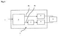
- Fig. 1 is a block diagram of a class-D amplifier/driver with delay in accordance with principles of the present invention.
- An analog or digital signal 1 is input for a signal treatment device 2.
- Output signals of said signal treatment device 2 are an inverted signal 8a and a non-inverted signal 8b.
- the polarity of the signals 8a, 8b are opposing each other.
- the signal 8 is input signal for output stages 4, 5.
- One of the signals, the inverted signal 8a or the non-inverted signal 8b, is applied to a delay element 3.
- the non-inverted signal 8b is applied to a delay element 3.
- the inverted signal 8a could be applied to the delay element 3.
- one of the signals 8a, 8b, the inverted or the non-inverted, of said signal treatment device 2 is applied with delay to the first output stage 4, the other one is applied without delay to the second output stage 5.
- Output pins of said first and second output stages 4, 5 are connected to a load 6.
- Said load 6 usually is a loudspeaker, earphone or the like, therefore a resistive, capacitive or inductive load.
- the signal for the first output stage 4 is delayed. Therefore, the two output pins often have the same voltage and no voltage drop is applied to the load 6. If the delay is small, the quality of the output signal stays the same as for the normal class-D structure.
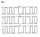
- Fig. 2 shows the outputs U 1 and U 2 of a standard class-D amplifier having the second output always at the opposite of the first output.
- the voltages U 1 and U 2 each correspond to one of the output pins of first and second output stage 4, 5.
- Current I L through a resistive load is always at a maximum value ( ⁇ I).
- Fig. 3 illustrates the output I L of a differential class-D amplifier with delay.
- the voltages U 1 and U 2 are not only alternating but also phase delayed. As shown in Fig. 3, there is no current I L through the load most of the time in the amplifier with delay according to the present invention.
- the output of the standard amplifier oscillates "clock-like".
- the delay time in the amplifier according to the present invention equal to the oscillation frequency, the power consumption goes to zero. In contrast to this, if the input stays at its maximum or minimum value, there is no reduction in power consumption.
- the power consumption depends about linear from the input signal amplitude, whereas for the standard amplifier the power consumption stays always at its maximum value.
- the power consumption of any class-D amplifier can be reduced.
- the reduction is even more important for class-D output drivers because they often have a load with a low resistivity.
- the tri-state output stage in accordance with the invention is also very advantageous for output drivers directly driven by a Sigma-Delta modulator.
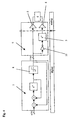
- the Sigma-Delta modulator 7 converts a high-resolution low frequency signal by a single-bit quantizer 8 into a low-resolution high frequency signal.
- a 16-bit signal sampled at 16 kHz is converted into a single-bit 2 MHz signal.
- a driver 9 comprising a second output stage 5 as a first path and an inverter 10, delay element 3 and first output stage 4 as a second path, a class-D style differential output driver can be accomplished.
- Said driver 9 corresponds to the amplifier/driver as illustrated in Fig. 1.
- Fig. 5 depicts a diagram showing total harmonic distortion and noise (THD+N) versus amplitude measurement on the output of an audio 16-bit Sigma-Delta Digital/Analog converter.
- a Line marked "two level output” shows the measurement of a state of the art amplifier as output driver, a line marked “three level output” shows the measurement of an amplifier according to the present invention as output driver. As shown in Fig.
- THD+N of an output driver according to the present invention is lower than THD+N of a state of the art output driver over nearly the whole volume range between -98dB and 0 dB. Only at very small and at very high amplitudes, near -98dB and 0dB, THD+N is about the same for a state of the art and an output driver according to the present invention.
Landscapes
- Engineering & Computer Science (AREA)
- Power Engineering (AREA)
- Amplifiers (AREA)
- Analogue/Digital Conversion (AREA)
Abstract
Claims (3)
- Amplificateur (7) comprenant un montage d'attaque comportant un premier étage de sortie (4) et un deuxième étage de sortie (5), l'amplificateur comprenant en outre un modulateur Sigma-Delta, le signal de sortie du modulateur Sigma-Delta étant un signal numérique appliqué comme signal d'entrée non inversé au premier étage de sortie (4) et inversé au deuxième étage de sortie (5), le signal de sortie du premier étage de sortie et du deuxième étage de sortie étant un signal numérique et le signal d'entrée étant appliqué avec un retard à l'un des étages de sortie (4, 5), caractérisé en ce que le retard est égal à 1/(fréquence suréchantillonnée).
- Utilisation d'un amplificateur selon la revendication 1 pour réduire la distorsion harmonique totale et le bruit d'un amplificateur classe D.
- Utilisation d'un amplificateur selon la revendication 1 pour réduire la puissance consommée par un amplificateur classe D.
Applications Claiming Priority (3)
| Application Number | Priority Date | Filing Date | Title |
|---|---|---|---|
| US40328602P | 2002-08-14 | 2002-08-14 | |
| US403286P | 2002-08-14 | ||
| PCT/EP2003/008945 WO2004017513A1 (fr) | 2002-08-14 | 2003-08-12 | Amplificateur |
Publications (2)
| Publication Number | Publication Date |
|---|---|
| EP1529340A1 EP1529340A1 (fr) | 2005-05-11 |
| EP1529340B1 true EP1529340B1 (fr) | 2006-03-22 |
Family
ID=31715969
Family Applications (1)
| Application Number | Title | Priority Date | Filing Date |
|---|---|---|---|
| EP03787772A Expired - Lifetime EP1529340B1 (fr) | 2002-08-14 | 2003-08-12 | Amplificateur classe d |
Country Status (6)
| Country | Link |
|---|---|
| EP (1) | EP1529340B1 (fr) |
| AU (1) | AU2003263214A1 (fr) |
| CA (2) | CA2494265C (fr) |
| DE (1) | DE60304213T2 (fr) |
| DK (1) | DK1529340T3 (fr) |
| WO (1) | WO2004017513A1 (fr) |
Families Citing this family (2)
| Publication number | Priority date | Publication date | Assignee | Title |
|---|---|---|---|---|
| JP4739189B2 (ja) * | 2004-04-14 | 2011-08-03 | 武田薬品工業株式会社 | 固形製剤 |
| EP2573938A1 (fr) * | 2011-09-22 | 2013-03-27 | Alcatel Lucent | Procédé d'amplification de signal basé sur une modulation à largeur d'impulsions |
Family Cites Families (7)
| Publication number | Priority date | Publication date | Assignee | Title |
|---|---|---|---|---|
| US4164714A (en) * | 1977-09-26 | 1979-08-14 | Harris Corporation | Polyphase PDM amplifier |
| JPS6059764B2 (ja) * | 1979-12-17 | 1985-12-26 | 松下電器産業株式会社 | 電力増幅器 |
| JP2000031810A (ja) * | 1998-07-10 | 2000-01-28 | Fujitsu Ltd | ドライバ回路 |
| WO2000007291A2 (fr) * | 1998-07-24 | 2000-02-10 | Toccata Technology Aps | Procede d'attenuation de distorsions et bruits lies au passage par zero dans un amplificateur, amplificateur et applications du procede et de l'amplificateur |
| US6262632B1 (en) * | 1999-11-16 | 2001-07-17 | Texas Instruments Incorporated | Concept and method to enable filterless, efficient operation of Class-D amplifiers |
| US20020060605A1 (en) * | 2000-09-22 | 2002-05-23 | Kowkutla Venkateswar R. | Amplifiers |
| US6605991B2 (en) * | 2001-08-30 | 2003-08-12 | Motorola, Inc. | Circuitry for creating a spectral null in a differential output switching amplifier and method therefor |
-
2003
- 2003-08-12 WO PCT/EP2003/008945 patent/WO2004017513A1/fr not_active Ceased
- 2003-08-12 DE DE60304213T patent/DE60304213T2/de not_active Expired - Lifetime
- 2003-08-12 AU AU2003263214A patent/AU2003263214A1/en not_active Abandoned
- 2003-08-12 DK DK03787772T patent/DK1529340T3/da active
- 2003-08-12 EP EP03787772A patent/EP1529340B1/fr not_active Expired - Lifetime
- 2003-08-12 CA CA2494265A patent/CA2494265C/fr not_active Expired - Lifetime
- 2003-08-14 CA CA 2437222 patent/CA2437222A1/fr not_active Abandoned
Also Published As
| Publication number | Publication date |
|---|---|
| CA2437222A1 (fr) | 2004-02-14 |
| DK1529340T3 (da) | 2006-06-12 |
| CA2494265A1 (fr) | 2004-02-26 |
| DE60304213D1 (de) | 2006-05-11 |
| DE60304213T2 (de) | 2007-03-29 |
| CA2494265C (fr) | 2010-06-01 |
| AU2003263214A1 (en) | 2004-03-03 |
| WO2004017513A1 (fr) | 2004-02-26 |
| EP1529340A1 (fr) | 2005-05-11 |
Similar Documents
| Publication | Publication Date | Title |
|---|---|---|
| KR100805437B1 (ko) | D급 증폭기 | |
| US8362832B2 (en) | Half-bridge three-level PWM amplifier and audio processing apparatus including the same | |
| US7446603B2 (en) | Differential input Class D amplifier | |
| US5835038A (en) | DC dither circuitry and method for delta-sigma modulator | |
| US7482865B2 (en) | Systems and methods for correcting errors resulting from component mismatch in a feedback path | |
| JP2006512004A (ja) | デジタル信号変調器を用いたデジタル入力信号の変調および信号の分割 | |
| US20020084843A1 (en) | Method and apparatus providing digital error correction for a class D power stage | |
| US20030030486A1 (en) | Pulse-width modulation circuit and power amplifier circuit | |
| JPH1155121A5 (fr) | ||
| US6940343B2 (en) | Amplifier | |
| TWI343173B (en) | Power amplifier and method for reducing common noise of power amplifier | |
| US6441760B2 (en) | Method and apparatus for digital to analog conversion | |
| CN114900136B (zh) | 用于测量连接到功率放大器的负载的电压和电流感测电路 | |
| US20020105377A1 (en) | Digital power amplifier | |
| US8816763B2 (en) | Integrator input error correction circuit and circuit method | |
| US6489840B2 (en) | Power amplification equipment | |
| US10790790B2 (en) | Amplifiers with delta-sigma modulators using pulse-density modulations and related processes | |
| US20050200405A1 (en) | Audio signal amplification method and apparatus | |
| US11750163B2 (en) | Deglitching circuit and method in a class-D amplifier | |
| CA2494265C (fr) | Amplificateur-etage d'attaque differentiel en classe d | |
| US20060232331A1 (en) | Segmented chopping amplifier | |
| US7023269B2 (en) | Digital amplifier and methods for enhancing resolution and dynamic range of a digital amplifier | |
| JP2005109590A (ja) | スイッチング増幅回路及びオーディオ機器用d級増幅装置 | |
| US11837999B2 (en) | Audio amplifier having idle mode | |
| US20220216835A1 (en) | Class-d amplifier, a method of generating a carrier wave signal in a class-d amplifier |
Legal Events
| Date | Code | Title | Description |
|---|---|---|---|
| PUAI | Public reference made under article 153(3) epc to a published international application that has entered the european phase |
Free format text: ORIGINAL CODE: 0009012 |
|
| 17P | Request for examination filed |
Effective date: 20050221 |
|
| AK | Designated contracting states |
Kind code of ref document: A1 Designated state(s): AT BE BG CH CY CZ DE DK EE ES FI FR GB GR HU IE IT LI LU MC NL PT RO SE SI SK TR |
|
| AX | Request for extension of the european patent |
Extension state: AL LT LV MK |
|
| 17Q | First examination report despatched |
Effective date: 20050517 |
|
| GRAP | Despatch of communication of intention to grant a patent |
Free format text: ORIGINAL CODE: EPIDOSNIGR1 |
|
| RTI1 | Title (correction) |
Free format text: CLASS D AMPLIFIER |
|
| DAX | Request for extension of the european patent (deleted) | ||
| RBV | Designated contracting states (corrected) |
Designated state(s): CH DE DK LI |
|
| GRAS | Grant fee paid |
Free format text: ORIGINAL CODE: EPIDOSNIGR3 |
|
| GRAA | (expected) grant |
Free format text: ORIGINAL CODE: 0009210 |
|
| AK | Designated contracting states |
Kind code of ref document: B1 Designated state(s): CH DE DK LI |
|
| REG | Reference to a national code |
Ref country code: CH Ref legal event code: EP |
|
| REF | Corresponds to: |
Ref document number: 60304213 Country of ref document: DE Date of ref document: 20060511 Kind code of ref document: P |
|
| REG | Reference to a national code |
Ref country code: DK Ref legal event code: T3 |
|
| REG | Reference to a national code |
Ref country code: CH Ref legal event code: PFA Owner name: AMI SEMICONDUCTOR SWITZERLAND SA Free format text: DSPFACTORY SA#CHAMPS-MONTANTS 12 A#2074 MARIN (CH) -TRANSFER TO- AMI SEMICONDUCTOR SWITZERLAND SA#CHAMPS-MONTANTS 12A#2074 MARIN-EPAGNIER (CH) Ref country code: CH Ref legal event code: NV Representative=s name: SOPRINTEL S.A. |
|
| PLBE | No opposition filed within time limit |
Free format text: ORIGINAL CODE: 0009261 |
|
| STAA | Information on the status of an ep patent application or granted ep patent |
Free format text: STATUS: NO OPPOSITION FILED WITHIN TIME LIMIT |
|
| 26N | No opposition filed |
Effective date: 20061227 |
|
| REG | Reference to a national code |
Ref country code: CH Ref legal event code: PUE Owner name: EMMA MIXED SIGNAL, CV Free format text: AMI SEMICONDUCTOR SWITZERLAND SA#CHAMPS-MONTANTS 12A#2074 MARIN-EPAGNIER (CH) -TRANSFER TO- EMMA MIXED SIGNAL, CV#TELESTONE 8, NARITAWEG 165#1043 BW AMSTERDAM (NL) |
|
| REG | Reference to a national code |
Ref country code: CH Ref legal event code: NV Representative=s name: STOLMSSR & PARTNER C/O GERNOT SPRINGER Ref country code: CH Ref legal event code: PUE Owner name: ON SEMICONDUCTOR TRADING LTD. Free format text: EMMA MIXED SIGNAL, CV#TELESTONE 8, NARITAWEG 165#1043 BW AMSTERDAM (NL) -TRANSFER TO- ON SEMICONDUCTOR TRADING LTD.#1 LANE HILL HAMMA BUILDING 3RD FLOOR#HAMILTON HM19 (BM) |
|
| REG | Reference to a national code |
Ref country code: DE Ref legal event code: R082 Ref document number: 60304213 Country of ref document: DE Representative=s name: STOLMAR SCHEELE & PARTNER, DE |
|
| REG | Reference to a national code |
Ref country code: CH Ref legal event code: PUE Owner name: SEMICONDUCTOR COMPONENTS INDUSTRIES, LLC Free format text: ON SEMICONDUCTOR TRADING LTD.#1 LANE HILL HAMMA BUILDING 3RD FLOOR#HAMILTON HM19 (BM) -TRANSFER TO- SEMICONDUCTOR COMPONENTS INDUSTRIES, LLC#5005 EAST MCDOWELL ROAD PHOENIX#ARIZONA 85008 (US) |
|
| REG | Reference to a national code |
Ref country code: DE Ref legal event code: R082 Ref document number: 60304213 Country of ref document: DE Representative=s name: STOLMAR & PARTNER PATENTANWAELTE PARTG MBB, DE Effective date: 20120711 Ref country code: DE Ref legal event code: R081 Ref document number: 60304213 Country of ref document: DE Owner name: SEMICONDUCTOR COMPONENTS INDUSTRIES, LLC, PHOE, US Free format text: FORMER OWNER: ON SEMICONDUCTOR TRADING LTD., HAMILTON, BM Effective date: 20120711 Ref country code: DE Ref legal event code: R082 Ref document number: 60304213 Country of ref document: DE Representative=s name: PATENTANWAELTE STOLMAR & PARTNER, DE Effective date: 20120711 |
|
| REG | Reference to a national code |
Ref country code: CH Ref legal event code: PCAR Free format text: NEW ADDRESS: SEEFELDSTRASSE 69, 8008 ZUERICH (CH) |
|
| PGFP | Annual fee paid to national office [announced via postgrant information from national office to epo] |
Ref country code: DK Payment date: 20150727 Year of fee payment: 13 |
|
| REG | Reference to a national code |
Ref country code: CH Ref legal event code: PFA Owner name: SEMICONDUCTOR COMPONENTS INDUSTRIES, LLC, US Free format text: FORMER OWNER: SEMICONDUCTOR COMPONENTS INDUSTRIES, LLC, US |
|
| REG | Reference to a national code |
Ref country code: DK Ref legal event code: EBP Effective date: 20160831 |
|
| PG25 | Lapsed in a contracting state [announced via postgrant information from national office to epo] |
Ref country code: DK Free format text: LAPSE BECAUSE OF NON-PAYMENT OF DUE FEES Effective date: 20160831 |
|
| REG | Reference to a national code |
Ref country code: CH Ref legal event code: PCAR Free format text: NEW ADDRESS: RUE DU CENDRIER 15 CP 1489, 1201 GENEVE (CH) |
|
| PGFP | Annual fee paid to national office [announced via postgrant information from national office to epo] |
Ref country code: DE Payment date: 20200710 Year of fee payment: 18 |
|
| PGFP | Annual fee paid to national office [announced via postgrant information from national office to epo] |
Ref country code: CH Payment date: 20200707 Year of fee payment: 18 |
|
| REG | Reference to a national code |
Ref country code: DE Ref legal event code: R119 Ref document number: 60304213 Country of ref document: DE |
|
| REG | Reference to a national code |
Ref country code: CH Ref legal event code: PL |
|
| PG25 | Lapsed in a contracting state [announced via postgrant information from national office to epo] |
Ref country code: LI Free format text: LAPSE BECAUSE OF NON-PAYMENT OF DUE FEES Effective date: 20210831 Ref country code: CH Free format text: LAPSE BECAUSE OF NON-PAYMENT OF DUE FEES Effective date: 20210831 |
|
| PG25 | Lapsed in a contracting state [announced via postgrant information from national office to epo] |
Ref country code: DE Free format text: LAPSE BECAUSE OF NON-PAYMENT OF DUE FEES Effective date: 20220301 |