EP1528678B1 - Comparateur - Google Patents
Comparateur Download PDFInfo
- Publication number
- EP1528678B1 EP1528678B1 EP04445101A EP04445101A EP1528678B1 EP 1528678 B1 EP1528678 B1 EP 1528678B1 EP 04445101 A EP04445101 A EP 04445101A EP 04445101 A EP04445101 A EP 04445101A EP 1528678 B1 EP1528678 B1 EP 1528678B1
- Authority
- EP
- European Patent Office
- Prior art keywords
- value
- counter
- clocked
- comparator
- circuit
- Prior art date
- Legal status (The legal status is an assumption and is not a legal conclusion. Google has not performed a legal analysis and makes no representation as to the accuracy of the status listed.)
- Expired - Lifetime
Links
- 238000000034 method Methods 0.000 claims description 16
- 230000003247 decreasing effect Effects 0.000 claims description 5
- 230000001419 dependent effect Effects 0.000 claims description 2
- 230000006399 behavior Effects 0.000 description 4
- 238000010586 diagram Methods 0.000 description 4
- 231100001261 hazardous Toxicity 0.000 description 3
- 230000001934 delay Effects 0.000 description 2
- 238000009434 installation Methods 0.000 description 1
- 230000001052 transient effect Effects 0.000 description 1
Images


Classifications
-
- H—ELECTRICITY
- H03—ELECTRONIC CIRCUITRY
- H03L—AUTOMATIC CONTROL, STARTING, SYNCHRONISATION OR STABILISATION OF GENERATORS OF ELECTRONIC OSCILLATIONS OR PULSES
- H03L7/00—Automatic control of frequency or phase; Synchronisation
- H03L7/06—Automatic control of frequency or phase; Synchronisation using a reference signal applied to a frequency- or phase-locked loop
-
- H—ELECTRICITY
- H03—ELECTRONIC CIRCUITRY
- H03M—CODING; DECODING; CODE CONVERSION IN GENERAL
- H03M1/00—Analogue/digital conversion; Digital/analogue conversion
- H03M1/06—Continuously compensating for, or preventing, undesired influence of physical parameters
- H03M1/08—Continuously compensating for, or preventing, undesired influence of physical parameters of noise
- H03M1/0863—Continuously compensating for, or preventing, undesired influence of physical parameters of noise of switching transients, e.g. glitches
- H03M1/0872—Continuously compensating for, or preventing, undesired influence of physical parameters of noise of switching transients, e.g. glitches by disabling changes in the output during the transitions, e.g. by holding or latching
-
- H—ELECTRICITY
- H03—ELECTRONIC CIRCUITRY
- H03K—PULSE TECHNIQUE
- H03K5/00—Manipulating of pulses not covered by one of the other main groups of this subclass
- H03K5/01—Shaping pulses
- H03K5/08—Shaping pulses by limiting; by thresholding; by slicing, i.e. combined limiting and thresholding
-
- H—ELECTRICITY
- H03—ELECTRONIC CIRCUITRY
- H03M—CODING; DECODING; CODE CONVERSION IN GENERAL
- H03M1/00—Analogue/digital conversion; Digital/analogue conversion
- H03M1/12—Analogue/digital converters
- H03M1/50—Analogue/digital converters with intermediate conversion to time interval
Definitions
- the present invention relates to an arrangement for setting or tuning a value in an integrated circuit and a method therefore. More specifically the present invention relates to an arrangement for securely setting or tuning a value in an integrated circuit wherein said value is set by increasing said value and detecting when a voltage depending on said value passes a threshold and a method therefore.
- One example of such an application could be to set, or tune, the operation point in a power amplifier transistor in a transmitter for a telecommunication application.
- the circuit should, by it self, after power up, tune in and hold the correct operation point for the power amplifier transistors in the transmitter.
- high demands regarding for instance reliability is put on telecommunication application and since the tuning and setting of the operating point for the power transistor is vital for the correct operation of the transistor it is highly important that a secure and reliable tuning and setting is performed.
- the comparator changes value the value of the counter is stored in a memory and is used as the value for, for instance the operating point for a power amplifier transistor.
- JP-A-56-94835 An example is shown in JP-A-56-94835 .
- Transients may cause the comparator to change value. Transients may be large compared to the measured value and may cause the comparator to indicate that the variable voltage has passed the reference voltage and thus that the optimal value has been reached, long before the system has tuned in. Noise may also contribute to erroneous changes of the comparator and thus false indications of optimal settings.
- a comparator circuit having a reference voltage input and a variable voltage input and being provided to produce a digital value on an output depending on a comparison between the reference voltage and the variable voltage, and a first clocked counter circuit connected to the comparator and provided to increase or decrease the value of the first clocked counter depending on the digital value supplied from the comparator.
- the arrangement further comprises a second clocked counter circuit connected to said comparator and being provided to increase the value of said second clocked counter for each change of value of said comparator, and a locking circuit connected to said second clocked counter circuit and provided to lock the value stored in said first clocked counter circuit from further changes when said second clocked counter reaches a first threshold value.
- a method for setting a value in an integrated circuit comprising a comparator having a first input for receiving a reference voltage, a second input for receiving a variable voltage, and a digital output.
- the method comprises the steps of comparing the variable voltage with the reference voltage to produce a digital value on the output of the comparator, which value is dependent on which of the variable voltage and reference voltage is greater, increasing a first counter if said digital value is a first value, decreasing said first counter if said digital value is a second value, increasing a second counter when said digital value changes from said first value to said second value or from said second value to said first value, and locking said first counter when said second counter is equal to, or greater than, a threshold value.
- the value of the first counter which should be used by the system to be controlled, is allowed to pass its optimal value a number of times before it is finally locked to its working value. That is, the value that should be used by the system during operation and which should be equal to, or at least as close as possible to, an optimal value, is allowed to close into its optimum, by swinging back and fourth, before it is locked. Thereby, a more reliable and more optimal value is achieved using a faster scheme. Further, the arrangement and method will not provide an erroneous value even in the presence of transients or noise.
- the first clocked counter is connected to a system to be controlled by the first clocked counter value, and the system to be controlled supplies a variable voltage to said variable voltage input on said comparator.
- the first clocked counter is, according to a preferred embodiment, connected to a system, such as a transmitter comprising a power amplifier transistor.
- the first clocked counter supplies a value to the system indicating an operating point for the power transistor.
- the system uses the received value as the operating point for the power transistor and measures the efficiency or performance of the power transistor, and converts this measure to a voltage level.
- This voltage level is thus an indication of how well the power transistor operates at the given operating point.
- This voltage level is supplied to the comparator as the variable voltage and is compared to the reference voltage.
- the comparator thus takes a value indicating if the value for the first clocked counter should be increased or decreased to achieve a better operating point, that is, an operating point that achieves a better performance for the power transistor.
- the comparator has changed sign a number of times, which is counted by the second clocked counter, the value of the first clocked counter is locked and this is the value used by the system as the operating point for the power transistor during operation
- the system may supply a value to a DC-converter, which converts the value to a DC voltage.
- the DC-voltage is then compared with the reference voltage.
- the arrangement and the method may be used to for instance, tune and set an operating point for a power amplifier transistor.
- the comparator is connected to the first and second clocked counter via a clocked sample-and-hold circuit, to reduce the risk of hazardous behaviour by the logic, for instance, so called "racing".
- the comparator is connected to the first clocked counter via a first sample-and-hold circuit, and the comparator is connected to the second clocked counter via a second sample-and-hold circuit, to further reduce the risk of hazardous behaviour by the logic, for instance, so called "racing"
- a clock generates a first clock pulse to the clocked sample-and-hold circuits, and a second and third clock pulse to the clocked counters, and the first, second and third clock pulses are generated sequentially and separated in time.
- a clock generates a first and third clock pulse to the clocked sample-and-hold circuits, and a second and third clock pulse to the clocked counters, and the first, second and third clock pulses are generated sequentially and separated in time.
- the digital value is a binary digital value.
- the first and second counters are clocked and said first counter is increased or decreased, respectively, for each clocking.
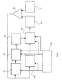
- Figure 1 is a schematic block diagram of a preferred embodiment according to the invention illustrating the main conceptual parts.
- Figure 2 is a schematic block diagram of a preferred embodiment according to the invention including a sample-and-hold block.
- Figure 3 is a schematic block diagram of a preferred embodiment according to the invention including two sample-and-hold blocks.
- Figure 1 is a schematic block diagram according to a preferred embodiment of the invention comprising a comparator 101 connected to a reference voltage 102 on a first input and a system 104, comprising a power amplifier transistor, on a second input.
- the system 104 supplies a voltage level to the comparator 101, which is compared with the reference voltage 102.
- the output from the comparator 101 is a binary digital number, or a logic level.
- the binary number takes a first value, for instance a logical one, when the voltage from the system 104 is less than the reference voltage 102, and takes a second value, for instance a logical zero, when voltage from the system 104 is greater than the reference voltage 102.
- the output from the comparator 101 is connected to a first counter 105, which is provided to increase its value for every clock cycle that the comparator takes the logical value 1 and decrease its value for every clock cycle that the comparator takes the logical value 0.
- the counter is further connected to the system 104.
- the system 104 uses the first counter value 105 for setting an operating point for a power amplifier transistor (not shown). This may be achieved using a digital-to-analogue converter converting the first counter value to a voltage level.
- the performance of the power amplifier transistor is measured and converted to a voltage indicating the performance of the so selected operating point for the power amplifier transistor.
- the optimal operating point in the system 104 for the power amplifier transistor will produce a value, which is equal to the reference voltage 102.
- the output from the comparator 101 is further connected to a second counter 106.
- the second counter 106 is provided to increase its value every time the comparator 101 changes value. That is, the value of the second counter 106 is increased every time the value on the comparators output changes from a logical one to a logical zero or vice versa. Thus, the second counter 106 registers every time the value of the first counter 105 passes the optimal value.
- the second counter 106 is further connected to a locking circuit 107.
- the locking circuit 107 which is connected to the first counter 105, locks the first counter 105 from further changes and the value of the first counter 105 can now be used by the system 104 for optimally setting the operating point for the power amplifier transistor.
- the tuning of the value of the first counter 105 By allowing the tuning of the value of the first counter 105 to pass the optimal setting a number of times before locking the first counter 105, the value is allowed to swing back and fourth closer to the optimum. Thereby, a faster clock frequency for clocking the circuits can be used and a generally quicker tuning and setting of the optimum value can be achieved.
- the embodiment described in connection with figure 1 may be fitted with a “sample-and-hold” circuit 201 and a six-phase clock 202 as disclosed in figure 2 .
- the sample-and-hold circuit 201 is provided to sample a value from the comparator 101 and store the value in a temporary storage.
- a clock signal, supplied by the six-phase clock 202 the value will be presented to the first and second counter 105 and 106, respectively.
- a DC-converter 103 is also disclosed for converting a value, indicating the performance of the system 104 with the value supplied by the first clocked counter 105, to a DC value, according to a preferred embodiment of the invention.
- the six-phase clock 202 is provided to supply three clock pulses, which are separated in time. That is, the six-phase clock 202 supplies a first clock pulse to the sample-and-hold circuit 201, waits a specified time, supplies a second clock pulse to the first and second counter 105 and 106, respectively, waits the specified time, supplies a third clock pulse to the first and second counter 105 and 106 and finally waits the specified time before starting over again. Thus, three clock pulses are generated and between each clock pulse a specified time is allowed to lapse before the next clock pulse.
- a first and a second "sample-and-hold" circuit 301 and 302, respectively are provided to sample and hold the value from the comparator 101 and to present the value to the first and second counter 105 and 106, respectively.
Landscapes
- Engineering & Computer Science (AREA)
- Theoretical Computer Science (AREA)
- Physics & Mathematics (AREA)
- Nonlinear Science (AREA)
- Amplifiers (AREA)
- Manipulation Of Pulses (AREA)
- Electronic Switches (AREA)
- Transmitters (AREA)
Claims (9)
- Disposition dans un circuit intégré, servant à fixer une valeur comportant un circuit comparateur doté d'une entrée de tension de référence et d'une entrée de tension variable et mis en place pour produire une valeur numérique sur une sortie dépendant d'une comparaison entre ladite tension de référence et ladite tension variable, et un premier circuit compteur cadencé relié audit comparateur et mis en place pour augmenter ou diminuer la valeur dudit compteur en fonction de la valeur numérique fournie à partir dudit comparateur,
caractérisée par- un deuxième circuit compteur cadencé relié audit comparateur et mis en place pour augmenter la valeur dudit deuxième circuit compteur cadencé pour chaque changement de valeur dudit comparateur, et- un circuit de blocage relié audit deuxième circuit compteur cadencé et mis en place pour bloquer tout changement supplémentaire de la valeur stockée dans ledit premier circuit compteur cadencé lorsque ledit deuxième circuit compteur cadencé atteint une première valeur de seuil. - Disposition selon la revendication 1,- ledit premier compteur cadencé comportant une sortie,- ladite sortie de premier compteur cadencé étant reliée à un système à commander par la valeur dudit premier compteur cadencé, et- ledit système à commander fournissant une tension variable à ladite entrée de tension variable dudit comparateur.
- Disposition selon la revendication 1,- ledit comparateur étant relié auxdits premier et deuxième compteurs cadencés par l'intermédiaire d'un circuit échantillonneur-bloqueur cadencé.
- Disposition selon la revendication 1,- ledit comparateur étant relié audit premier compteur cadencé par l'intermédiaire d'un premier circuit échantillonneur-bloqueur, et- ledit comparateur étant relié audit deuxième compteur cadencé par l'intermédiaire d'un deuxième circuit échantillonneur-bloqueur.
- Disposition selon la revendication 3 ou 4,- une horloge générant une première impulsion d'horloge vers lesdits circuits échantillonneurs-bloqueurs cadencés, une deuxième et une troisième impulsions d'horloge vers lesdits compteurs cadencés, et- lesdites première, deuxième et troisième impulsions d'horloge étant générées séquentiellement et espacées dans le temps.
- Disposition selon la revendication 3 ou 4,- une horloge générant une première et une troisième impulsions d'horloge vers lesdits circuits échantillonneurs-bloqueurs cadencés, une deuxième et une troisième impulsions d'horloge vers lesdits compteurs cadencés, et- lesdites première, deuxième et troisième impulsions d'horloge étant générées séquentiellement et espacées dans le temps.
- Procédé pour fixer une valeur dans un circuit intégré comportant un comparateur doté d'une première entrée destinée à recevoir une tension de référence, d'une deuxième entrée destinée à recevoir une tension variable et d'une sortie numérique, ledit procédé comportant les étapes consistant à :- comparer ladite tension variable à ladite tension de référence pour produire une valeur numérique sur ladite sortie, ladite valeur étant déterminée par le fait que la tension la plus élevée soit ladite tension variable ou ladite tension de référence,- augmenter un premier compteur si ladite valeur numérique est une première valeur,- diminuer ledit premier compteur si ladite valeur numérique est une deuxième valeur,ledit procédé étant caractérisé par :- l'augmentation d'un deuxième compteur lorsque ladite valeur numérique passe de ladite première valeur à ladite deuxième valeur ou de ladite deuxième valeur à ladite première valeur, et- le blocage dudit premier compteur lorsque ledit deuxième compteur est supérieur ou égal à une valeur de seuil.
- Procédé selon la revendication 7,- ladite valeur numérique étant une valeur numérique binaire.
- Procédé selon la revendication 7,- lesdits premier et deuxième compteurs étant cadencés et ledit premier compteur étant respectivement augmenté ou diminué à chaque cadencement.
Applications Claiming Priority (2)
| Application Number | Priority Date | Filing Date | Title |
|---|---|---|---|
| SE0302861 | 2003-10-30 | ||
| SE0302861A SE526369C2 (sv) | 2003-10-30 | 2003-10-30 | Komparator |
Publications (3)
| Publication Number | Publication Date |
|---|---|
| EP1528678A2 EP1528678A2 (fr) | 2005-05-04 |
| EP1528678A3 EP1528678A3 (fr) | 2007-01-03 |
| EP1528678B1 true EP1528678B1 (fr) | 2008-03-19 |
Family
ID=29580163
Family Applications (1)
| Application Number | Title | Priority Date | Filing Date |
|---|---|---|---|
| EP04445101A Expired - Lifetime EP1528678B1 (fr) | 2003-10-30 | 2004-10-01 | Comparateur |
Country Status (7)
| Country | Link |
|---|---|
| US (1) | US7057422B2 (fr) |
| EP (1) | EP1528678B1 (fr) |
| JP (1) | JP2005137008A (fr) |
| KR (1) | KR100742008B1 (fr) |
| CN (1) | CN100483927C (fr) |
| DE (1) | DE602004012512T2 (fr) |
| SE (1) | SE526369C2 (fr) |
Families Citing this family (6)
| Publication number | Priority date | Publication date | Assignee | Title |
|---|---|---|---|---|
| CN1329786C (zh) * | 2005-07-28 | 2007-08-01 | 深圳兆日技术有限公司 | 一种避免字典攻击的方法 |
| US9363262B1 (en) * | 2008-09-15 | 2016-06-07 | Galileo Processing, Inc. | Authentication tokens managed for use with multiple sites |
| CN103427806A (zh) * | 2012-05-16 | 2013-12-04 | 浙江科跃焊接设备有限公司 | 具有信号锁定功能的电压比较器 |
| US8653868B2 (en) * | 2012-06-28 | 2014-02-18 | Intel Corporation | Low power data recovery |
| CN105981405A (zh) * | 2013-12-25 | 2016-09-28 | 怀斯迪斯匹有限公司 | 使用静电式传声器的系统和方法 |
| US9780870B1 (en) * | 2014-09-30 | 2017-10-03 | National Technology & Engineering Solutions Of Sandia, Llc | Integrated unaligned resonant modulator tuning |
Family Cites Families (8)
| Publication number | Priority date | Publication date | Assignee | Title |
|---|---|---|---|---|
| FR2333247A1 (fr) | 1975-11-25 | 1977-06-24 | Thomson Csf | Circuit de comparaison de frequences et dispositif de selection comportant un tel circuit |
| JPS5694835A (en) * | 1979-12-28 | 1981-07-31 | Ricoh Co Ltd | A/d converter |
| EP0111607B1 (fr) * | 1982-12-10 | 1986-05-21 | Merrell Toraude Et Compagnie | Tropyl- et pseudotropylalkyl benzoates, et leur application pour le traitement de migraines |
| DE3606893A1 (de) * | 1986-03-03 | 1987-09-10 | Zdzislaw Gulczynski | Analog-digital-wandler |
| JP3171474B2 (ja) | 1992-01-20 | 2001-05-28 | 株式会社東芝 | 同調回路 |
| US5761255A (en) * | 1995-11-30 | 1998-06-02 | The Boeing Company | Edge-synchronized clock recovery unit |
| US6242908B1 (en) * | 1996-01-17 | 2001-06-05 | Allegro Microsystems, Inc. | Detection of passing magnetic articles while adapting the detection threshold |
| JPH09247220A (ja) | 1996-03-01 | 1997-09-19 | Kokusai Electric Co Ltd | 自動周波数制御回路 |
-
2003
- 2003-10-30 SE SE0302861A patent/SE526369C2/sv unknown
-
2004
- 2004-10-01 DE DE602004012512T patent/DE602004012512T2/de not_active Expired - Lifetime
- 2004-10-01 EP EP04445101A patent/EP1528678B1/fr not_active Expired - Lifetime
- 2004-10-19 US US10/968,671 patent/US7057422B2/en not_active Expired - Fee Related
- 2004-10-29 JP JP2004316364A patent/JP2005137008A/ja not_active Withdrawn
- 2004-10-29 CN CNB200410095940XA patent/CN100483927C/zh not_active Expired - Fee Related
- 2004-10-30 KR KR1020040087575A patent/KR100742008B1/ko not_active Expired - Fee Related
Also Published As
| Publication number | Publication date |
|---|---|
| US7057422B2 (en) | 2006-06-06 |
| JP2005137008A (ja) | 2005-05-26 |
| CN100483927C (zh) | 2009-04-29 |
| EP1528678A3 (fr) | 2007-01-03 |
| DE602004012512T2 (de) | 2009-04-16 |
| DE602004012512D1 (de) | 2008-04-30 |
| SE526369C2 (sv) | 2005-08-30 |
| KR100742008B1 (ko) | 2007-07-23 |
| SE0302861D0 (sv) | 2003-10-30 |
| US20050093724A1 (en) | 2005-05-05 |
| CN1612466A (zh) | 2005-05-04 |
| KR20050041987A (ko) | 2005-05-04 |
| SE0302861L (sv) | 2005-05-01 |
| EP1528678A2 (fr) | 2005-05-04 |
Similar Documents
| Publication | Publication Date | Title |
|---|---|---|
| US6157690A (en) | Digital PLL circuit | |
| US7602223B2 (en) | Delay-locked loop circuit and method of generating multiplied clock therefrom | |
| US7952391B2 (en) | Digital noise filter | |
| US8552775B2 (en) | Digital phase-locked loop apparatus using frequency shift keying and method of controlling the same | |
| US10979057B1 (en) | Delay lock loop and phase locking method thereof | |
| US7969214B2 (en) | DLL circuit, update control apparatus in DLL circuit and update method of DLL circuit | |
| US6687844B1 (en) | Method for correcting clock duty cycle skew by adjusting a delayed clock signal according to measured differences in time intervals between phases of original clock signal | |
| EP1528678B1 (fr) | Comparateur | |
| CN101588177A (zh) | 数字锁定指示器、锁相环频率综合器及无线收发机 | |
| US8847639B1 (en) | Waveform generator | |
| US8513994B2 (en) | State machine for deskew delay locked loop | |
| US11509314B2 (en) | All-digital phase-locked loop | |
| US5977837A (en) | Phase selector for external frequency divider and phase locked loop | |
| US9673833B1 (en) | Aligning asynchronous signals by time shifting information | |
| GB2493251A (en) | Calibration of the timing of the latching of ADC output data | |
| US8222920B2 (en) | Dynamic phase alignment | |
| KR20030048043A (ko) | 듀얼에지 m/n 카운터 | |
| US7956649B1 (en) | Frequency pattern detector | |
| US7911859B2 (en) | Delay line and memory control circuit utilizing the delay line | |
| US11916476B2 (en) | Voltage generator and voltage generating method thereof | |
| US20050046603A1 (en) | Fast digital data recovery circuit | |
| US11588490B2 (en) | Digital loop filter in all-digital phase-locked loop | |
| US6553088B1 (en) | Digital delay phase locked loop | |
| CN120281319A (zh) | 逐次逼近型模数转换器的亚稳态错误现场校正电路 | |
| CN117040529A (zh) | 一种适用于倍频延迟锁相环的错误锁定保护电路 |
Legal Events
| Date | Code | Title | Description |
|---|---|---|---|
| PUAI | Public reference made under article 153(3) epc to a published international application that has entered the european phase |
Free format text: ORIGINAL CODE: 0009012 |
|
| AK | Designated contracting states |
Kind code of ref document: A2 Designated state(s): AT BE BG CH CY CZ DE DK EE ES FI FR GB GR HU IE IT LI LU MC NL PL PT RO SE SI SK TR |
|
| AX | Request for extension of the european patent |
Extension state: AL HR LT LV MK |
|
| PUAL | Search report despatched |
Free format text: ORIGINAL CODE: 0009013 |
|
| AK | Designated contracting states |
Kind code of ref document: A3 Designated state(s): AT BE BG CH CY CZ DE DK EE ES FI FR GB GR HU IE IT LI LU MC NL PL PT RO SE SI SK TR |
|
| AX | Request for extension of the european patent |
Extension state: AL HR LT LV MK |
|
| RIC1 | Information provided on ipc code assigned before grant |
Ipc: H03M 1/38 20060101ALN20061124BHEP Ipc: H03M 1/08 20060101ALI20061124BHEP Ipc: H03K 3/00 20060101AFI20050131BHEP |
|
| 17P | Request for examination filed |
Effective date: 20070130 |
|
| GRAP | Despatch of communication of intention to grant a patent |
Free format text: ORIGINAL CODE: EPIDOSNIGR1 |
|
| RIC1 | Information provided on ipc code assigned before grant |
Ipc: H03M 1/56 20060101ALI20070514BHEP Ipc: H03K 5/08 20060101ALI20070514BHEP Ipc: H03M 1/08 20060101ALI20070514BHEP Ipc: H03M 1/38 20060101ALN20070514BHEP Ipc: H03K 3/00 20060101AFI20070514BHEP |
|
| AKX | Designation fees paid |
Designated state(s): DE |
|
| GRAS | Grant fee paid |
Free format text: ORIGINAL CODE: EPIDOSNIGR3 |
|
| GRAA | (expected) grant |
Free format text: ORIGINAL CODE: 0009210 |
|
| AK | Designated contracting states |
Kind code of ref document: B1 Designated state(s): DE |
|
| REF | Corresponds to: |
Ref document number: 602004012512 Country of ref document: DE Date of ref document: 20080430 Kind code of ref document: P |
|
| PLBE | No opposition filed within time limit |
Free format text: ORIGINAL CODE: 0009261 |
|
| STAA | Information on the status of an ep patent application or granted ep patent |
Free format text: STATUS: NO OPPOSITION FILED WITHIN TIME LIMIT |
|
| 26N | No opposition filed |
Effective date: 20081222 |
|
| PGFP | Annual fee paid to national office [announced via postgrant information from national office to epo] |
Ref country code: DE Payment date: 20171216 Year of fee payment: 14 |
|
| REG | Reference to a national code |
Ref country code: DE Ref legal event code: R119 Ref document number: 602004012512 Country of ref document: DE |
|
| PG25 | Lapsed in a contracting state [announced via postgrant information from national office to epo] |
Ref country code: DE Free format text: LAPSE BECAUSE OF NON-PAYMENT OF DUE FEES Effective date: 20190501 |