EP1528668A2 - Amplifier and frequency converter - Google Patents
Amplifier and frequency converter Download PDFInfo
- Publication number
- EP1528668A2 EP1528668A2 EP04022665A EP04022665A EP1528668A2 EP 1528668 A2 EP1528668 A2 EP 1528668A2 EP 04022665 A EP04022665 A EP 04022665A EP 04022665 A EP04022665 A EP 04022665A EP 1528668 A2 EP1528668 A2 EP 1528668A2
- Authority
- EP
- European Patent Office
- Prior art keywords
- feedback
- phase
- circuit
- signal
- amplifier
- Prior art date
- Legal status (The legal status is an assumption and is not a legal conclusion. Google has not performed a legal analysis and makes no representation as to the accuracy of the status listed.)
- Withdrawn
Links
Images


Classifications
-
- H—ELECTRICITY
- H03—ELECTRONIC CIRCUITRY
- H03F—AMPLIFIERS
- H03F1/00—Details of amplifiers with only discharge tubes, only semiconductor devices or only unspecified devices as amplifying elements
- H03F1/08—Modifications of amplifiers to reduce detrimental influences of internal impedances of amplifying elements
- H03F1/22—Modifications of amplifiers to reduce detrimental influences of internal impedances of amplifying elements by use of cascode coupling, i.e. earthed cathode or emitter stage followed by earthed grid or base stage respectively
-
- H—ELECTRICITY
- H03—ELECTRONIC CIRCUITRY
- H03F—AMPLIFIERS
- H03F1/00—Details of amplifiers with only discharge tubes, only semiconductor devices or only unspecified devices as amplifying elements
- H03F1/34—Negative-feedback-circuit arrangements with or without positive feedback
-
- H—ELECTRICITY
- H03—ELECTRONIC CIRCUITRY
- H03F—AMPLIFIERS
- H03F3/00—Amplifiers with only discharge tubes or only semiconductor devices as amplifying elements
- H03F3/189—High-frequency amplifiers, e.g. radio frequency amplifiers
- H03F3/19—High-frequency amplifiers, e.g. radio frequency amplifiers with semiconductor devices only
-
- H—ELECTRICITY
- H03—ELECTRONIC CIRCUITRY
- H03F—AMPLIFIERS
- H03F3/00—Amplifiers with only discharge tubes or only semiconductor devices as amplifying elements
- H03F3/45—Differential amplifiers
- H03F3/45071—Differential amplifiers with semiconductor devices only
- H03F3/45076—Differential amplifiers with semiconductor devices only characterised by the way of implementation of the active amplifying circuit in the differential amplifier
- H03F3/4508—Differential amplifiers with semiconductor devices only characterised by the way of implementation of the active amplifying circuit in the differential amplifier using bipolar transistors as the active amplifying circuit
- H03F3/45085—Long tailed pairs
- H03F3/45089—Non-folded cascode stages
-
- H—ELECTRICITY
- H03—ELECTRONIC CIRCUITRY
- H03F—AMPLIFIERS
- H03F2200/00—Indexing scheme relating to amplifiers
- H03F2200/144—Indexing scheme relating to amplifiers the feedback circuit of the amplifier stage comprising a passive resistor and passive capacitor
-
- H—ELECTRICITY
- H03—ELECTRONIC CIRCUITRY
- H03F—AMPLIFIERS
- H03F2200/00—Indexing scheme relating to amplifiers
- H03F2200/372—Noise reduction and elimination in amplifier
-
- H—ELECTRICITY
- H03—ELECTRONIC CIRCUITRY
- H03F—AMPLIFIERS
- H03F2200/00—Indexing scheme relating to amplifiers
- H03F2200/492—A coil being added in the source circuit of a transistor amplifier stage as degenerating element
-
- H—ELECTRICITY
- H03—ELECTRONIC CIRCUITRY
- H03F—AMPLIFIERS
- H03F2203/00—Indexing scheme relating to amplifiers with only discharge tubes or only semiconductor devices as amplifying elements covered by H03F3/00
- H03F2203/45—Indexing scheme relating to differential amplifiers
- H03F2203/45256—One or more reactive elements are added in the source circuit of the amplifying FETs of the dif amp
-
- H—ELECTRICITY
- H03—ELECTRONIC CIRCUITRY
- H03F—AMPLIFIERS
- H03F2203/00—Indexing scheme relating to amplifiers with only discharge tubes or only semiconductor devices as amplifying elements covered by H03F3/00
- H03F2203/45—Indexing scheme relating to differential amplifiers
- H03F2203/45464—Indexing scheme relating to differential amplifiers the CSC comprising one or more coils
Definitions
- the present invention relates to amplifiers for amplifying an input signal, and frequency converters for amplifying an input signal and then converting the frequency of the amplified signal. More specifically, the present invention relates to an amplifier and a frequency converter both having a wide dynamic range and suitable for integration into a semiconductor integrated circuit.
- a signal received at an antenna is amplified by an amplifier circuit at an initial stage.
- Such an initial-stage amplifier circuit is required to have characteristics of achieving low noise and high gain when receiving a weak signal, while achieving low distortion and low gain when receiving a large signal.
- a wider dynamic range is required than ever in a receiving system.
- a widely used scheme is inserting a resistance between a signal line and the ground at the input or output of the amplifier circuit.
- insertion of the resistance at the input side causes severe degradation in noise characteristics.
- Insertion of the resistance at the output side causes severe degradation in distortion characteristics.
- Other known schemes for stabilizing the operation of the amplifier circuit include a scheme of applying negative feedback to the input. That is, in this scheme, a signal shifted in phase by 180 degrees is fed back to the input. According to this scheme, it is possible to achieve an amplifier circuit generally having a wide dynamic range, although noise and distortion characteristics are both slightly degraded.
- a negative feedback circuit used in this scheme can also operate as a distortion compensator circuit, thereby making the dynamic range still wider with some contrivances of the circuit configuration.
- a first conventional example is a "negative feedback power amplifier" disclosed in Japanese Laid-Open Patent Publication No. 10-22751 (1998-22751) (see FIG. 15).
- the amplifier as illustrated in FIG. 15 includes a negative feedback circuit which is capable of operating as a distortion compensator circuit and is used in a microwave band.
- transistors 601 and 602 are both field-effect transistors.
- Inductors 603, 604, and 605, and capacitors 606 and 607 form a matching circuit for the transistors 601 and 602.
- a microstrip line 608 serves as a phase shifter.
- a power voltage Vcc is applied via the microstrip line 608 to the amplifier.
- Part of an output signal from the transistor 602 is fed via the inductor 605, the microstrip line 608, and then the inductor 604 back to the input of the transistor 601.
- a length L of the microstrip line 608 is adjusted so that the feedback signal and the output signal from the transistor 602 are different in phase from each other by 180 degrees. With part of the output signal including a distortion component being inverted in phase for feedback to the input, distortion characteristics in a high frequency band can be improved.
- a second conventional example is a "high-output amplifier" disclosed in Japanese Laid-Open Patent Publication No. 6-216670 (1994-216670) (see FIG. 16).
- the amplifier as illustrated in FIG. 16 includes strip lines 701a and 701b as signal lines, a signal-amplifying transistor 702, a directional coupler 703, a feedback strip line 704, a stub 705, resistances 706a and 706b for changing the amount of feedback, a level detector circuit 707, a harmonic suppression controller circuit 708, and a terminator resistance 709.
- an input supplied via the signal-line strip line 701a is amplified by the signal-amplifying transistor 702.
- An output from the transistor 702 is fed, via the feedback strip line 704 having a predetermined line length and then the directional coupler 703, back to the input of the signal-amplifying transistor 702 for signal amplification.
- fed back to the input of the signal-amplifying transistor 702 is a signal opposite in phase to a second harmonic. As such, with the distortion of the second harmonic being cancelled, the linearity of the signal-amplifying transistor 702 can be improved.
- a third conventional example is an "amplifier" disclosed in PCT International Publication No. WO96/25791 (see FIG. 17).
- the amplifier as illustrated in FIG. 17 includes a transistor 801, signal sources 802 and 803, a signal source resistance 804, an input matching circuit composed of components denoted by 805, 806, 807, 808, and809, an output matching circuit composed of components denoted by 810, 811, and 815, a band-pass filter 812, aphaseshifter 813, a variable attenuator 814, and a load resistance 816.
- the band-pass filter 812 passes a second harmonic of an output from the transistor 801.
- the phase shifter 813 and the variable attenuator 814 adjust the phase and amplitude of the second harmonic, respectively.
- the second harmonic of the output signal is fed back to the input, thereby reducing the third-order intermodulation product of the amplifier.
- a fourth conventional example is a "power amplifier" disclosed in Japanese Laid-Open Patent Publication No. 7-94954 (1995-94954) (see FIG. 18).
- the amplifier as illustrated in FIG. 18 includes a combiner 901, a power amplifier 902, a divider 903, a filter 904, a variable phase shifter 905, and a variable attenuator 906.
- This amplifier phase-shifts a fundamental wave and higher order waves (a second or third- or fourth-order harmonic, etc.) of the output from the power amplifier 902 by 180 degrees in a wide band, and the resultant wave is fed back to the input of the power amplifier 902.
- the fundamental wave and the second harmonic of the output from the power amplifier 902 being negatively fed back to the input, it is possible to compensate for distortion of the output signal.
- a fifth conventional example is a "wide-band feedback amplifier" disclosed in Japanese Laid-Open Patent Publication 10-335954 (1998-335954) (see FIG. 19).
- the amplifier as illustrated in FIG. 19 includes an amplifying device 1001, a signal input 1002, a signal output 1003, a slot line ground plane 1004, a slot line openplane 1005, a strip line 1006, amicrostrip line 1007 in a slot line conversion part, a slot line 1008, via holes 1009, through holes 1010, and a resistance 1011 for determining the amount of feedback.
- this amplifier shifts the phase of the output from the amplifying device 1001 by 180 degrees in a wide band, and then feeds the results back to the input of the amplifying device 1001.
- the gazette of this publication discloses a specific example of a feedback circuit for phase shift by 180 degrees in a wide band.
- a sixth conventional example is a "broadband amplification with high linearity and low power consumption" disclosed in PCT International Publication No. WO00/45505 (see FIG. 20).
- the amplifier as illustrated in FIG. 20 includes an input transistor 1101, an output transistor 1102, a series reactive feedback network 1103, and a shunt reactive feedback network 1104.
- the input transistor 1101 and the output transistor 1102 are coupled in a cascode configuration with the input transistor defining an input of the amplifier and the output transistor defining an output of the amplifier.
- the shunt reactive feedback network 1104 is coupled between the input and the output and is characterized by an impedance of substantially zero resistance and non-zero reactance.
- the above first through sixth conventional examples have a drawback that due to only one type of shunt feedback path being provided for each conventional example, the feedback circuit is complex in structure and large in size in order to shift the feedback signal in phase by approximately 180 degrees with respect to the input signal.
- the second harmonic is shifted in phase by almost 360 degrees for feedback to the input. Therefore, this amplifier does not perform distortion compensation by negative feedback of the second harmonic.
- the fundamental wave is barely fed back. Therefore, these amplifiers do not perform distortion compensation by negative feedback of the third-order intermodulation wave occurring at a frequency in the vicinity of the frequency of the fundamental wave.
- a process of phase adjustment made to both of the fundamental wave and the harmonic is performed only by the feedback circuit, thereby making the feedback circuit complex in structure and large in size.
- an object of the present invention is to provide a negative feedback amplifier and a negative feedback frequency converter each of simple structure, capable of providing negative feedback of the phases of a fundamental wave and a third-order intermodulation wave of an input signal to the input, and suitable for integration into a semiconductor integrated circuit. Further, another object of the present invention is to provide a negative feedback amplifier and a negative feedback frequency converter capable of providing negative feedback of a phase of a second harmonic of the input signal to the input, in addition to the fundamental wave and the third-order intermodulation wave of the input signal.
- the present invention has the following features to attain the object mentioned above.
- An amplifier of the present invention comprises: an amplifier circuit for amplifying an input signal; a first feedback circuit for feeding a feedback output of the amplifier circuit back to an input of the amplifier circuit while changing a phase of the signal; and a second feedback circuit for feeding an output of the amplifier circuit back to the input of the amplifier circuit while changing a phase of the signal.
- the amplifier of the present invention includes an amplifier to which a single-ended signal is inputted and an amplifier to which a differential signal composed of an in-phase signal and an opposite-phase signal is inputted.
- each of the amplifier circuit, the first feedback circuit, and the second feedback circuit inputs and outputs the single-ended signal.
- the first feedback circuit a circuit including an inductor (or a circuit in which an inductor and a capacitor are connected to each other in parallel) being connected to a feedback terminal of the amplifier circuit and a ground; and a capacitor being connected to the feedback terminal and an input terminal is used.
- a circuit formed by connecting a capacitor in series to a circuit in which a resistance and a capacitor are connected to each other in parallel, a circuit formed by connecting a capacitor in parallel to a circuit in which a resistance and a capacitor are connected to each other in series, or a circuit in which a resistance or an inductor is placed between a connecting point of two capacitors being connected to each other in series and a ground is used.
- the amplifier circuit includes: an in-phase amplifying section having an in-phase input terminal and an in-phase feedback terminal and operating based on an in-phase signal; and an opposite-phase amplifying section having an opposite-phase input terminal and an opposite-phase feedback terminal and operating based on an opposite-phase signal
- the first feedback circuit includes one or more feedback sections
- the second feedback circuit includes: an in-phase feedback section operating based on the in-phase signal; and an opposite-phase feedback section operating based on the opposite-phase signal.
- the in-phase feedback section and the opposite-phase feedback section may include a circuit formed by connecting a capacitor in series to a circuit in which a resistance and a capacitor are connected to each other in parallel, a circuit formed by connecting a capacitor in parallel to a circuit in which a resistance and a capacitor are connected in series, or a circuit in which a resistance or an inductor is placed between a connecting point of two capacitors being connected to each other in series and a ground.
- a wireless receiver of the present invention comprises: the amplifier of the present invention for amplifying a reception signal received by an antenna; the frequency converter of the present invention for converting a frequency of an output of the amplifier; an interfering signal determination section for making a determination on an interfering signal for the reception signal; and a control section for changing consumption current in the amplifier and the frequency converter based on the determination result in the interfering signal determination section.
- a fundamental wave, a third-order intermodulation wave, and a second harmonic of the input signal can be negatively fed back with a simple structure. Therefore, it is possible to provide an amplifier having a wide dynamic range.
- a fundamental wave, a third-order intermodulation wave, and a second harmonic of the input signal can be negatively fed back with a simple structure in the case where a nondifferential signal is inputted.
- the above-stated first feedback circuit it is possible to adjust the passing phase in the amplifier circuit by appropriately selecting the value of the inductor (or the values of the inductor and the capacitor) .
- the first feedback circuit having the inductor and the capacitor, a phase control over the fundamental wave and the second harmonic can be more flexibly performed.
- a cascode amplifier circuit (or a single-type amplifier circuit) can be used for amplifying an input signal.
- an amplifier having low noise characteristics can be achieved.
- the above-stated second feedback circuit it is possible to adjust the passing phase in the second feedback circuit by appropriately selecting characteristics of each component element of the second feedback circuit.
- a fundamental wave, a third-order intermodulation wave, and a second harmonic of the input signal can be negatively fed back with a simple structure in the case where a differential signal is inputted.
- the amplifier to which a differential signal is inputted has the effect similar to that of the amplifier to which a single-ended signal is inputted.
- the fundamental wave, the third-order intermodulation wave, and the second harmonic of the input signal can be negatively fed back with high flexibility.
- the fundamental wave, the third-order intermodulation wave, and the second harmonic of the input signal can be negatively fed back with a simple structure while differential circuits in the differential amplifier circuit keep forming a good pair.
- a fundamental wave, a third-order intermodulation wave, and a second harmonic of the input signal can be negatively fed back with a simple structure. Therefore, it is possible to provide a frequency converter having a wide dynamic range. Also, according to the wireless terminal of the present invention, it is possible to widen a dynamic range of the amplifier and the frequency converter while minimizing the increase in the consumption current.
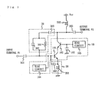
- FIG. 1 is a circuit diagram of an amplifier according to a first embodiment of the present invention.
- the amplifier as shown in FIG. 1 includes an amplifier circuit 10, a first feedback circuit 20, a second feedback circuit 30, a DC cut capacitors 501 and 503, and a choke inductor 502.
- This amplifier has a feature where the operations of the first feedback circuit 20 and the second feedback circuit 30 cause a phase of a signal in which fundamental waves included in two feedback signals are combined and a phase of a signal in which second harmonics included in two feedback signals are combined to be shifted by approximately 180 degrees from a phase of a fundamental wave of an input signal.
- the amplifier is used mainly in a high frequency band.
- the amplifier circuit 10 includes bipolar transistors 101 and 102, a bypass capacitor 103, and bias circuits 104 and 105.
- the amplifier circuit 10 amplifies a signal inputted from an input terminal P1.
- the first feedback circuit 20 includes an inductor 201 and a capacitor 202.
- the first feedback circuit 20 feeds the output from the emitter (a feedback terminal of the amplifier circuit 10) of the bipolar transistor 101 included in the amplifier circuit 10 back to the input of the amplifier circuit 10.
- the inductor 201 and the capacitor 202 are used for adjusting the passing phase of the first feedback circuit 20.
- the second feedback circuit 30 includes a resistance 301, a capacitor 302, and a DC cut capacitor 303, so as to feed the output from the collector (an output terminal of the amplifier circuit 10) of the bipolar transistor 102 included in the amplifier circuit 10 back to the input of the amplifier circuit 10.
- the resistance 301 and the capacitor 302 are used for adjusting the passing phase of the second feedback circuit 30.
- the input terminal P1 is connected via the DC cut capacitor 501 to the base of the bipolar transistor 101.
- the collector of the bipolar transistor 101 is connected to the emitter of the bipolar transistor 102, whereas the collector of the bipolar transistor 102 is connected via the DC cut capacitor 503 to an output terminal P2.
- the emitter of the bipolar transistor 101 is grounded via the inductor 201.
- the capacitor 202 is inserted between the base and emitter of the bipolar transistor 101.
- the bases of the bipolar transistors 101 and 102 are supplied with a base current from the bias circuits 104 and 105, respectively.
- the resistance 301 and the capacitor 302 are connected to each other in parallel.
- This parallel circuit and the DC cut capacitor 303 are inserted in series between the base of the bipolar transistor 101 and the collector of the bipolar transistor 102.
- the base of the bipolar transistor 102 is grounded via the bypass capacitor 103.
- a power voltage Vcc is supplied via the choke inductor 502 to the collector of the bipolar transistor 102.
- FIGS. 2A through 2F the operation of the amplifier as illustrated in FIG. 1 will be described below.
- passing phase characteristics are studied below on the following three circuits: a circuit as illustrated in FIG. 2A including the bipolar transistor 101, the inductor 201, and the capacitor 202; a circuit as illustrated in FIG. 2B including the bipolar transistors 101 and 102, the bypass capacitor 103, the inductor 201, the resistance 301, and the capacitor 302; and a circuit as illustrated in FIG. 2C having therein the circuit as illustrated in FIG. 2B to which the capacitor 202 is added.
- FIG. 2D is a phasor diagram of an input signal (a fundamental wave) and an output signal (a fundamental wave and a second harmonic) in the circuit as illustrated in FIG. 2A.
- a fundamental wave S 1a included in the feedback signal outputted from a terminal P4 leads a fundamental wave S 0 of a signal inputted to a terminal P3 by a phase angle of ⁇ a .
- a second harmonic S 2a included in the feedback signal outputted from the terminal P4 leads the fundamental signal S 0 of the input signal by a phase angle of 2 ⁇ a .
- a ratio of lead in the passing phase is determined by the values of the inductor 201 and the capacitor 202.
- FIG. 2E is a phasor diagram of an input signal (a fundamental wave) and an output signal (a fundamental wave and a second harmonic) in the circuit as illustrated in FIG. 2B.
- a fundamental wave S 1b included in the feedback signal outputted from a terminal P5 lags behind the fundamental wave S 0 of the signal inputted to the terminal P3 by a phase angle of ⁇ b .
- a second harmonic S 2b included in the feedback signal outputted from the terminal P5 lags behind the fundamental wave S 0 of the input signal by a phase angle of 2 ⁇ b .
- a ratio of delay in the passing phase is determined by the values of the resistance 301 and the capacitor 302.
- FIG. 2F is a phasor diagram of an input signal (a fundamental wave) and an output signal (a fundamental wave and a second harmonic) in the circuit as illustrated in FIG. 2C. Illustrated in FIG. 2F is vector addition for calculating a synthesis signal of the feedback signals as illustrated in FIGS. 2D and 2E (hereinafter, referred to as a synthesis feedback signal). According to FIG. 2F, the synthesis feedback signal includes (S 1a +S 1b ) as a fundamental wave component, and (S 2a +S 2b ) as a second harmonic component.
- the circuit as illustrated in FIG. 2C has two feedback paths.
- the inductor 201, the capacitors 202 and 302, and the resistance 301 it is possible to shift the phase of the fundamental wave (S 1a +S 1b ) included in the synthesis feedback signal and the phase of the second harmonic (S 2a +S 2b ) included in the synthesis feedback signal from the phase of the fundamental wave S 0 of the input signal by approximately 180 degrees as illustrated in FIG. 2F.
- the amplifier as illustrated in FIG. 1 can feed the second harmonic shifted in phase by 180 degrees back to the input. That is, the second harmonic can be negatively fed back to the input.
- the frequency of the third-order intermodulation wave is adjacent to the frequency of the fundamental wave. Therefore, the amplifier of the present embodiment can feed the third-order intermodulation wave shifted in phase by 180 degrees back to the input. That is, the third-order intermodulation wave can be negatively fed back to the input.
- the passing phase of the first feedback circuit 20 is adjusted by the inductor 201 and the capacitor 202, whereas the passing phase of the second feedback circuit 30 is adjusted by the resistance 301 and the capacitor 302.
- the amplifier of the present embodiment does not use a strip line or slot line, compared with the conventional amplifiers. Therefore, the amplifier can be easily integrated, even if being used in a microwave band, into a semiconductor integrated circuit.
- the first feedback circuit 20 and the second feedback circuit 30 are used so as to appropriately adjust the phase of the feedback signal. With this, it is possible to achieve, on the entire amplifier, negative feedback of the fundamental wave, the third-order intermodulation wave, and the second harmonic of the input signal. Thus, a high-frequency negative feedback amplifier having a wide dynamic range can be achieved with a simple structure.
- FIG. 3 is a circuit diagram of an amplifier according to a second embodiment of the present invention.
- the amplifier as illustrated in FIG. 3 differs from that according to the first embodiment in that it is structured by a differential pair.
- the operation and effect of the amplifier which will be described below are similar to those of the amplifier according to the first embodiment, and therefore descriptions thereof are omitted.
- only the circuit configuration will be described.
- the amplifier as illustrated in FIG. 3 includes an amplifier circuit 15, a first feedback circuit 25, a second feedback circuit 35, DC cut capacitors 501a, 501b, 503a, and 503b, and choke inductors 502a and 502b.
- the amplifier circuit 15, the first feedback circuit 25, and the second feedback circuit 35 are exemplary modifications of the amplifier circuit 10, the first feedback circuit 20, and the second feedback circuit 30 according to the first embodiment, each of which is structured by a differential pair.
- the amplifier circuit 15 includes bipolar transistors 101a, 101b, 102a, and 102b, and bias circuits 104 and 105.
- the amplifier circuit 15 amplifies a differential signal input via a pair of input terminals ⁇ P1+, P1- ⁇ .
- the first feedback circuit 25 includes inductors 201a and 201b and capacitors 202a and 202b. These inductors 201a and 201b and the capacitors 202a and 202b are used for adjusting the passing phase of the first feedback circuit 25.
- the second feedback circuit 35 includes resistances 301a and 301b, capacitors 302a and 302b, and DC cut capacitors 303a and 303b, so as to feed the output of the amplifier circuit 15 back to the input thereof.
- the resistances 301a and 301b and the capacitors 302a and 302b are used for adjusting the passing phase of the second feedback circuit 35. Note that, in the differential circuit, it is possible to achieve the same effect as a bypass capacitor of a nondifferential circuit only by connecting a pair of transistors. Thus, the amplifier circuit 15 does not need to include a bypass capacitor separately.
- the input terminal P1+ is connected via the DC cut capacitor 501a to the base of the bipolar transistor 101a, whereas the input terminal P1-is connected via the DC cut capacitor 501b to the base of the bipolar transistor 101b.
- the collectors of the bipolar transistors 101a and 101b are connected to the emitters of the bipolar transistors 102a and 102b, respectively.
- the collector of the bipolar transistor 102a is connected via the DC cut capacitor 503a to an output terminal P2+, whereas the collector of the bipolar transistor 102b is connected via the DC cut capacitor 503b to an output terminal P2-.
- the emitters of the bipolar transistors 101a and 101b are connected to the inductors 201a and 201b, respectively, at one end each. At the other end each, the inductors 201a and 201b are connected to each other, and their connecting point Q1 is grounded.
- the capacitor 202a is inserted between the base and emitter of the bipolar transistor 101a, whereas the capacitor 202b is inserted between the base and emitter of the bipolar transistor 101b.
- the base of each of the bipolar transistors 101a and 101b is supplied with a base current from the bias circuit 104.
- the base of each of the bipolar transistors 102a and 102b is supplied with a base current from the bias circuit 105.
- the resistance 301a and the capacitor 302a are connected to each other in parallel so as to form a parallel circuit.
- This parallel circuit and the DC cut capacitor 303a are inserted in series between the base of the bipolar transistor 101a and the collector of the bipolar transistor 102a.
- the resistance 301b and the capacitor 302b are connected to each other in parallel so as to form a parallel circuit.
- This parallel circuit and the DC cut capacitor 303b are inserted in series between the base of the bipolar transistor 101b and the collector of the bipolar transistor 102b.
- the power voltage Vcc is supplied via the choke inductors 502a and 502b to the collectors of the bipolar transistors 102a and 102b, respectively.
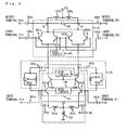
- FIG. 4 is a circuit diagram of an amplifier according to a third embodiment of the present invention.
- the amplifier as illustrated in FIG. 4 is similar to that according to the second embodiment, except that the first feedback circuit 25 is replaced by a first feedback circuit 26. Therefore, in FIG. 4, components similar to those according to the second embodiment are provided with the same reference numerals, and are not described herein.
- the first feedback circuit 26 includes inductors 201a, 201b, and 203, and capacitors 202a and 202b.
- the emitters of the bipolar transistors 101a and 101b are connected to the inductors 201a and 201b, respectively, at one end each.
- the inductors 201a and 201b are connected to each other, and their connecting point Q2 is grounded via the inductor 203.
- the capacitor 202a is inserted between the emitter and base of the bipolar transistor 101a, whereas the capacitor 202b is inserted between the emitter and base of the bipolar transistor 101b.
- the inductor 203 is used for adjusting the passing phase of the second harmonic of the first feedback circuit 26.
- the first feedback circuit 26 is supplied with a differential signal. Therefore, at the connecting point Q2, two input signals are cancelled by each other. The potential at the connecting point Q2 is always 0 even though the input signals are alternating-current signals. Therefore, the passing phase of a fundamental wave component of the output signal is not influenced by the inductor 203.
- FIG. 5A a circuit as illustrated in FIG. 5A including the bipolar transistors 101a and 101b, the inductors 201a, 201b, and 203, and the capacitors 202a and 202b; a circuit as illustrated in FIG. 5B including the bipolar transistors 101a, 101b, 102a, and 102b, the inductors 201a, 201b, and 203, the resistances 301a and 301b, and the capacitors 302a and 302b; and a circuit as illustrated in FIG. 5C having therein the circuit as illustrated in FIG. 5B to which the capacitors 202a and 202b are added.
- FIG. 5D is a phasor diagram of an input signal (a fundamental wave) and an output signal (a fundamental wave and a second harmonic) in the circuit as illustrated in FIG. 5A.
- a fundamental wave S 1c included in the feedback signal outputted from terminals P4+ and P4- leads a fundamental wave So of a signal inputted to terminals P3+ and P3-by a phase angle of ⁇ c .
- a second harmonic S 2c included in the feedback signal outputted from the terminals P4+ and P4- leads the fundamental signal So of the input signal by a phase angle of 2 ⁇ c ' ( ⁇ 2 ⁇ c ).
- FIG. 5E is a phasor diagram of an input signal (a fundamental wave) and an output signal (a fundamental wave and a second harmonic) in the circuit as illustrated in FIG. 5B.
- a fundamental wave S 1d included in the feedback signal outputted from terminals P5+ and P5- lags behind a fundamental wave So of a signal inputted to terminals P3+ and P3- by a phase angle of ⁇ d .
- FIG. 5F is a phasor diagram of an input signal (a fundamental wave) and an output signal (a fundamental wave and a second harmonic) in the circuit as illustrated in FIG. 5C. Illustrated in FIG. 5F is vector addition for calculating a synthesis signal of the feedback signals as illustrated in FIGS. 5D and 5E (hereinafter, referred to as a synthesis feedback signal) . According to FIG. 5F, the synthesis feedback signal includes (S 1c +S 1d ) as a fundamental wave component, and (S 2c +S 2d ) as a second harmonic component.
- the circuit as illustrated in FIG. 5C has two feedback paths.
- the inductors 201a, 201b, and 203, the capacitors 202a, 202b, 302a, and 302b, and the resistances 301a and 301b it is possible to shift the phase of the fundamental wave (S 1c +S 1d ) included in the synthesis feedback signal and the phase of the second harmonic (S 2c +S 2d ) included in the synthesis feedback signal from the phase of the fundamental wave So of the input signal by approximately 180 degrees as illustrated in FIG. 5F.
- the amplifier as illustrated in FIG. 4 can negatively feed the second harmonic back to the input.
- the frequency of the third-order intermodulation wave is adjacent to the frequency of the fundamental wave. Therefore, the amplifier of the present embodiment can negatively feed the third-order intermodulation wave back to the input.
- the passing phase of the first feedback circuit 26 is adjusted by the inductors 201a, 201b, and 203 and the capacitors 202a and 202b, whereas the passing phase of the second feedback circuit 35 is adjusted by the resistances 301a and 301b and the capacitors 302a and 302b.
- the amplifier according to the third embodiment further includes the inductor 203 for separately adjusting the second harmonic component.
- the inductor 203 for separately adjust the passing phase of each of the fundamental wave, the third-order intermodulation wave, and the second harmonic of the input signal with a simple structure. Therefore, it is possible, for example, to select the values of the inductors 201a and 201b in advance so that other high-frequency characteristics, such as noise characteristics, are optimal, and then select the value of the inductor 203.
- a high-frequency negative feedback amplifier having a wide dynamic range can be achieved with more flexibility than that of the amplifier of the second embodiment.
- FIG. 6 is a circuit diagram of an amplifier according to a fourth embodiment of the present invention.
- the amplifier as illustrated in FIG. 6 is similar to that according to the second embodiment, except that the first feedback circuit 25 is replaced by a first feedback circuit 27. Therefore, in FIG. 6, components similar to those according to the second embodiment are provided with the same reference numerals, and are not described herein.
- the first feedback circuit 27 includes the capacitors 202a and 202b, and an inductor 204. Unlike the second embodiment, the emitters of the bipolar transistors 101a and 101b are directly connected to each other, and their connecting point Q3 is grounded via the inductor 204. The inductor 204 is used for adjusting the passing phase of the second harmonic of the amplifier circuit.
- the operations of the resistances 301a and 301b and the capacitors 202a, 202b, 302a, and 302b cause the fundamental wave shifted in phase by 180 degrees to be fed back to the input. That is, the fundamental wave can be negatively fed back to the input.
- the operation of the inductor 204 causes the second harmonic shifted in phase by 180 degrees to be fed back to the input. That is, the second harmonic can be negatively fed back.
- the frequency of the third-order intermodulation wave is adjacent to the frequency of the fundamental wave. Therefore, the amplifier can feed the third-order intermodulation wave shifted in phase by 180 degrees back to the input. That is, the third-order intermodulation wave can be negatively fed back to the input.
- the passing phase of the first feedback circuit 27 is adjusted by the capacitors 202a and 202b and the inductor 204, whereas the passing phase of the second feedback circuit 35 is adjusted by the resistances 301a and 301b and the capacitors 302a and 302b. Therefore, it is possible to achieve negative feedback of the fundamental wave, the third-order intermodulation wave, and the second harmonic of the input signal to the input with a simple structure.
- a differential amplifier circuit it is preferable that two differential circuits form a good pair, that is, the characteristics (DC and AC characteristics) of these differential circuits as a pair in the differential amplifier circuit are close to each other.
- the differential circuits do not always form a good pair due to variations in stray capacitance, parasitic resistance, etc.
- the inductors 201a and 201b are not used. Therefore, it is possible to achieve an effect that the differential circuits can keep forming a good pair.
- the amplifier of the present embodiment with the inductors 201a and 201b not being provided, it is possible to achieve a high-frequency negative feedback amplifier having a wide dynamic range while the differential circuits in the differential amplifier circuit keep forming a good pair.
- FIG. 7 is a circuit diagram of a frequency converter according to a fifth embodiment of the present invention.
- the frequency converter as illustrated in FIG. 7 includes the amplifier circuit 10, the first feedback circuit 20, the second feedback circuit 30, a frequency converter circuit 40, DC cut capacitors 501, 503a, 503b, 504a, and 504b, and choke inductors 502a and 502b.
- This frequency converter is structured by adding the frequency converter circuit 40 to the amplifier according to the first embodiment.
- components similar to those according to the first embodiment are provided with the same reference numerals, and are not described herein.
- the frequency converter circuit 40 includes bipolar transistors 401 and 402, a bias circuit 403, and a capacitor 404, thereby converting the frequency of a signal supplied by the amplifier circuit 10.
- the input terminal P1 is connected via the DC cut capacitor 501 to the base of the bipolar transistor 101.
- the collector of the bipolar transistor 101 is connected to the emitter of the bipolar transistor 102.
- the collector of the bipolar transistor 102 is connected to both of the emitters of the bipolar transistors 401 and 402.
- the collector of the bipolar transistor 401 is connected via the DC cut capacitor 503a to an output terminal P3+, whereas the collector of the bipolar transistor 402 is connected via the DC cut capacitor 503b to an output terminal P3-.
- the emitter of the bipolar transistor 101 is grounded via the inductor 201.
- the capacitor 202 is inserted between the base and emitter of the bipolar transistor 101.
- the bases of the bipolar transistors 101 and 102 are supplied with a base current from the bias circuits 104 and 105, respectively.
- the base of each of the bipolar transistors 401 and 402 is supplied with a base current from the bias circuit 403.
- the resistance 301 and the capacitor 302 are connected to each other in parallel. This parallel circuit and the DC cut capacitor 303 are inserted in series between the base of the bipolar transistor 101 and the collector of the bipolar transistor 102. The base of the bipolar transistor 102 is grounded via the bypass capacitor 103. The collectors of the bipolar transistors 401 and 402 are supplied with a power voltage Vcc via the choke inductors 502a and 502b, respectively.
- An input terminal P2+ is connected via the DC cut capacitor 504a to the base of the bipolar transistor 401, whereas an input terminal P2- is connected via the DC cut capacitor 504b to the base of the bipolar transistor 402.
- the capacitor 404 is inserted between the collectors of the bipolar transistors 401 and 402 for reducing a leak of the second harmonic of a local signal to the output terminals P3+ and P3-.
- the input terminal P1 is supplied with an RF (Radio Frequency) signal received by an antenna and then amplified by a low-noise amplifier.
- the input terminals P2+ and P2- are supplied with a LO (Local Oscillator) signal supplied by a local oscillator.
- Output from the output terminals P3+ and P3- is an IF (Intermediate Frequency) signal mainly including a signal of an intermediate frequency.
- the frequency converter as illustrated in FIG. 7 can feed back the fundamental signal and the second harmonic that have been shifted in phase by 180 degrees of the RF signal supplied by the input terminal P1. That is, the fundamental signal and the second harmonic can be negatively fed back to the input.
- the frequency of the third-order intermodulation wave is adjacent to the frequency of the fundamental wave. Therefore, the frequency converter can feed the third-order intermodulation wave shifted in phase by 180 degrees back to the input. That is, the third-order intermodulation wave can be negatively fed back to the input.
- the passing phase of the first feedback circuit 20 is adjusted by the inductor 201 and the capacitor 202, whereas the passing phase of the second feedback circuit 30 is adj ustedby the resistance 301 and the capacitor 302. Therefore, it is possible to achieve negative feedback of the fundamental wave, the third-order intermodulation wave, and the second harmonic of the input signal to the input with a simple structure.
- the frequency converter of the present embodiment does not use a strip line or slot line, compared with conventional frequency converters. Therefore, the frequency converter can be easily integrated, even if being used in a microwave band, into a semiconductor integrated circuit.
- the first feedback circuit 20 and the second feedback circuit 30 are used to appropriately adjust the phase of the feedback signal, thereby achieving, on the entire frequency converter, negative feedback of the fundamental wave, the third-order intermodulation wave, and the second harmonic of the input signal. Therefore, a high-frequency negative feedback frequency converter having a wide dynamic range can be achieved with a simple structure.
- FIG. 8 is a circuit diagram of a frequency converter according to a sixth embodiment of the present invention.
- the frequency converter as illustrated in FIG. 8 differs from that according to the fifth embodiment in that it is structured by a differential pair.
- the operation and effect of the frequency converter are similar to those of the frequency converter according to the fifth embodiment, and therefore descriptions thereof are omitted.
- only the circuit configuration will be described.
- the frequency converter as illustrated in FIG. 8 includes an amplifier circuit 15, a first feedback circuit 25, a second feedback circuit 35, a frequency converter circuit 45, DC cut capacitors 501a, 501b, 503a, 503b, 504a, and 504b, and choke inductors 502a and 502b.
- the amplifier circuit 15, the first feedback circuit 25, and the second feedback circuit 35 are exemplary modifications of the amplifier circuit 10, the first feedback circuit 20, and the second feedback circuit 30 according to the fifth embodiment, each of which is structured by a differential pair.
- the amplifier circuit 15, the first feedback circuit 25, and the second feedback circuit 35 are similar to those of the frequency converter according to the second embodiment, and therefore descriptions thereof are omitted.
- the frequency converter circuit 45 includes bipolar transistors 401a, 401b, 402a, and 402b, a bias circuit 403, and a capacitor 404, and converts the frequency of an output signal from the amplifier circuit 15.
- an input terminal P1+ is connected via the DC cut capacitor 501a to the base of the bipolar transistor 101a, whereas an input terminal P1- is connected via the DC cut capacitor 501b to the base of the bipolar transistor 101b.
- the collector of the bipolar transistor 101a is connected to the emitter of the bipolar transistor 102a, whereas the collector of the bipolar transistor 101b is connected to the emitter of the bipolar transistor 102b.
- the collector of the bipolar transistor 102a is connected to both of the emitters of the bipolar transistors 401a and 402a.
- the collector of the bipolar transistor 102b is connected to both of the emitters of the bipolar transistors 401b and 402b.
- the collectors of the bipolar transistors 401a and 401b are connected at a connecting point R1, whereas the collectors of the bipolar transistors 402a and 402b are connected at a connecting point R2.
- the connecting point R1 is connected via the DC cut capacitor 503a to an output terminal P3+, whereas the connecting point R2 is connected via the DC cut capacitor 503b to an output terminal P3-.
- the emitters of the bipolar transistors 101a and 101b are connected to the inductors 201a and 201b, respectively, at one end each. At the other end each, the inductors 201a and 201b are connected to each other, and their connecting point Q1 is grounded.
- the capacitor 202a is inserted between the base and emitter of the bipolar transistor 101a, whereas the capacitor 202b is inserted between the base and emitter of the bipolar transistor 101b.
- the base of each of the bipolar transistors 101a and 101b is supplied with a base current from the bias circuit 104.
- the base of each of the bipolar transistors 102a and 102b is supplied with a base current from the bias circuit 105.
- the base of each of the bipolar transistors 401a, 401b, 402a, and 402b is supplied with a base current from the bias circuit 403.
- the resistance 301a and the capacitor 302a are connected to each other in parallel so as to form a parallel circuit.
- This parallel circuit and the DC cut capacitor 303a are inserted in series between the base of the bipolar transistor 101a and the collector of the bipolar transistor 102a.
- the resistance 301b and the capacitor 302b are connected to each other in parallel so as to form a parallel circuit.
- This parallel circuit and the DC cut capacitor 303b are inserted in series between the base of the bipolar transistor 101b and the collector of the bipolar transistor 102b.
- the power voltage Vcc is supplied via the choke inductors 502a and 502b to the connecting points R1 and R2, respectively.
- An input terminal P2+ is connected via the DC cut capacitor 504a to each of the bases of the bipolar transistors 401a and 402b.
- An input terminal P2- is connected via the DC cut capacitor 504b to each of the bases of the bipolar transistors 401b and 402a.
- the capacitor 404 is inserted between the connecting points R1 and R2 for reducing a leak of the second harmonic of a local signal to the output terminals P3+ and P3-.
- FIG. 9 is a circuit diagram of a frequency converter according to a seventh embodiment of the present invention.
- the frequency converter as illustrated in FIG. 9 is similar to that according to the sixth embodiment, except that the first feedback circuit 25 is replaced by a first feedback circuit 26.
- a high-frequency negative feedback frequency converter having a wide dynamic range can be achieved with more flexibility than that of the frequency converter of the sixth embodiment with a simple structure.
- FIG. 10 is a circuit diagram of a frequency converter according to an eighth embodiment of the present invention.
- the frequency converter as illustrated in FIG. 10 is similar to that according to the sixth embodiment, except that the first feedback circuit 25 is replaced by a first feedback circuit 27.
- a high-frequency negative feedback frequency converter having a wide dynamic range can be achieved while the differential circuits of the differential amplifier circuit keep forming a good pair.
- each of the second feedback circuit 30 and 35 as shown in each embodiment can be replaced by another feedback circuit.
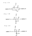
- a feedback circuit can be formed by using any of three circuits as illustrated in FIGS. 11A through 11C.
- a circuit 31 as illustrated in FIG. 11A includes a resistance 311 and capacitors 312 and 313. The resistance 311 and the capacitor 312 are connected to each other in series to form a series circuit, to which the capacitor 313 is connected in parallel.
- a circuit 32 as illustrated in FIG. 11B includes capacitors 321 and 322, and a resistance 323. The capacitors 321 and 322 are connected to each other in series, and their connecting point S1 is grounded via the resistance 323.
- a circuit 33 as illustrated in FIG. 11C includes capacitors 331 and 332, and an inductor 333. The capacitors 331 and 332 are connected in series, and their connecting point S2 is grounded via the inductor 333.
- the feedback circuit as illustrated in FIG. 11A is used to form the amplifier according to the first embodiment.
- a terminal P7 is connected to the base of the bipolar transistor 101, whereas a terminal P8 is connected to the collector of the bipolar transistor 102.
- the second feedback circuit 35 which is structured by a differential pair, can be formed by using a pair of two circuits, both identical to one of three circuits as illustrated in FIGS. 11A through 11C.
- a feedback signal may vary in amplitude and phase depending on, for instance, a level of an input signal.
- a variable-capacitance diode (see FIG. 12) may be replaced by the capacitor in the feedback circuit.
- a first feedback circuit 29 includes a variable-capacitance diode 252
- a second feedback circuit 39 includes a variable-capacitance diode 352. Voltages of impedance control signals Vctl1 and Vctl2 change with a level of an input signal, for example.
- a change in the voltage of the impedance control signal Vctl1 causes the capacitance value of the variable-capacitance diode 352 to change, whereas a change in the voltage of the impedance control signal Vctl2 causes the capacitance value of the variable-capacitance diode 252 to change.
- a feedback signal varies in amplitude and phase.
- an amplifier circuit having another structure can be used instead of the cascode amplifier circuit 10 or 15 in each embodiment.
- a single-type amplifier circuit see FIG. 13
- an amplifier circuit 11 includes a bipolar transistor 101 and a bias circuit 104.
- the collector of the bipolar transistor 101 is connected via the DC cut capacitor 503 to the output terminal P2.
- the amplifier of FIG. 13 is similar to that according to the first embodiment. With the use of such a single-type amplifier circuit, an amplifier having low noise characteristics can be achieved. The above same effects can be also achieved by applying a single-type amplifier circuit to the amplifiers and the frequency converters of other embodiments.
- the bipolar transistors as shown in each embodiment can be replaced by heterojunction bipolar transistors made of SiGe/Si, AlGaAs/GaAs, or GaInP/GaAs.
- the bipolar transistors can be replaced by MOSFETs.
- Such replaceable bipolar transistors are those provided with reference numerals of 101 and 102 as shown in FIG. 1, 101a, 101b, 102a, and 102b as shown in FIGS. 3, 4, and 6, 101, 102, 401, and 402 as shown in FIG. 7, and 101a, 101b, 102a, 102b, 401a, 401b, 402a, and 402b as shown in FIGS. 8, 9, and 10.
- the first feedback circuits 20, 25, 26, and 27 are implemented by inductors and capacitors.
- the inductor instead of the inductor, a circuit in which the inductor and the capacitor are connected to each other in parallel can be used. With this, a phase control over the fundamental wave and the second harmonic can be more flexibly performed.
- replaceable inductors are those provided with reference numerals of 201 as shown in FIGS. 1 and 7, 201a and 201b as shown in FIGS. 3 and 8, 201a, 201b, and 203 as shown in FIGS. 4 and 9, and 204 as shown in FIGS. 6 and 10.
- the resistances by polysilicon are those provided with reference numerals of 301 in FIGS. 1 and 7, and 301a and 301b in FIGS. 3, 4, 6, 8, 9, and 10.
- Such capacitors preferably implemented by MOS capacitors or the like are those provided with reference numerals of 103, 202, 302, and 303 in FIG.
- such inductors preferably implemented by wiring layers are those provided with reference numerals of 201 in FIGS. 1 and 7, 201a and 201b in FIGS. 3 and 8, 201a, 201b, and 202 in FIGS. 4 and 9, and 204 in FIGS. 6 and 10.
- the phase of the feedback signal in the amplifiers and the frequency converters according to the above embodiments is influenced by an impedance of the signal source side seen from the device and an impedance of the load side seen from the device. Therefore, when a matching circuit is used at the input or output of the amplifiers and the frequency converters according to the above embodiments, the first and second feedback circuits have to be designed in consideration of the impedance of the matching circuit, so that a phase difference between the input signal and the feedback signal of each of the fundamental wave and the second harmonic is 180 degrees.
- thepassingphase of the first feedback circuit and the passing phase of the second feedback circuit are both adjusted.
- the fundamental wave, the third-order intermodulation wave, and the second harmonic of the input signal can be negatively fed back to the input on the whole amplifier and frequency converter. Therefore, it is possible to achieve a high-frequency negative feedback amplifier and a high-frequency negative feedback frequency converter each having a wide dynamic range with a simple structure.
- FIG. 14 is an illustration showing a structure of a wireless terminal according to a ninth embodiment of the present invention.
- a wireless terminal performing transmission and reception simultaneously, a portion of a transmission signal generated by a transmission circuit is leaked to a reception circuit when transmission is performed.
- an amplifier and a frequency converter included in the reception circuit are required to have a very wide dynamic range.
- the amplifier and the frequency converter included in the reception circuit are required to consume a small current.
- the wireless terminal includes an amplifier 42 according to the first to fourth embodiments and the modifications thereof and a frequency converter 80 according to the fifth to eighth embodiments and the modifications thereof. Also, the wireless terminal includes a control section 90 for changing consumption current in the amplifier 42 and the frequency converter 80.
- the control section 90 When a transmission start signal is received from a transmission baseband circuit 12, the control section 90 turns a modulator 13 and an amplifier 41 ON. As a result, the level of a leakage signal leaked from the transmission circuit to the reception circuit is increased. Thus, the control section 90 performs control so as to increase the consumption current in the amplifier 42 and the frequency converter 80 when the transmission start signal is received from the transmission baseband circuit 12.
- the amplifier 42 and the frequency converter 80 are a negative feedback amplifier and a negative feedback frequency converter, respectively. Thus, even if the consumption current is increased, the gains of the amplifier 42 and the frequency converter 80 are not significantly increased. As a result, it is possible to realize a wireless terminal having a wide dynamic range without a major change in the level diagram structure of the wireless terminal.
- the transmission baseband circuit 12, the modulator 13, the amplifier 41, an isolator 50, and a filter 51 comprise the transmission circuit
- filters 52 to 54, amplifiers 42 and 70, a signal generator 60, the frequency converter 80, a demodulator 21, and a reception baseband circuit 22 comprise the reception circuit.
- a leakage signal leaked from the transmission circuit to the reception circuit becomes an interfering signal for the reception circuit.
- the transmission baseband circuit 12 functions as a transmission signal generation section
- the control section 90 functions as an interfering signal determination section and a control section.
- the transmission baseband circuit 12 generates a transmission signal
- the modulator 13 modulates the transmission signal outputted from the transmission baseband circuit 12.
- the demodulator 21 demodulates a reception signal outputted from the filter 54
- the reception baseband circuit 22 performs a predetermined process for the reception signal outputted from the demodulator 21.
- the amplifiers 41, 42, and 70 amplify an input signal, and the filters 51 to 54 performfiltering of an input signal.
- the isolator 50 passes a signal in one direction.
- the signal generator 60 generates a signal having a predetermined frequency.
- the frequency converter 80 mixes two input signals.
- the antenna 9 performs transmission and reception of electric waves.
- the control section 90 turns the modulator 13 and the amplifier 41 ON, and performs control so as to increase the consumption current in the amplifier 42 and the frequency converter 80.
- the control section 90 performs control so as to increase a bias voltage of the bias circuit included in the amplifier as shown in FIG. 1, or increase a bias voltage of the bias circuit included in the frequency converter as shown in FIG. 7.
- the consumption current in the amplifier 42 and the frequency converter 80 is increased, and the level of distortion of the amplifier 42 and the frequency converter 80 is increased.
- the consumption current in the amplifier 42 and the frequency converter 80 is controlled so as to be high.
- a wireless receiver and a wireless reception method of the present invention will be described by describing an operation of the wireless terminal as shown in FIG. 14.
- the operation of the wireless terminal will be divided into three parts: transmission, reception, and control. Note that, in actuality, these three parts are executed simultaneously.
- the wireless terminal of present embodiment even if a communication scheme performing transmission and reception simultaneously (e.g., W-CDMA scheme) is adopted, it is possible to widen a dynamic range of the amplifier and the frequency converter while minimizing the increase in the consumption current. As such, it is possible to concurrently achieve a wide dynamic range and reduced consumption current.
- a communication scheme performing transmission and reception simultaneously e.g., W-CDMA scheme
- the amplifier and the frequency converter of the present invention each have a wide dynamic range with a simple structure. Therefore, the amplifier and the frequency converter of the present invention can be used as various types of amplifiers and frequency converters such as receivers of a wireless communication system.
Landscapes
- Engineering & Computer Science (AREA)
- Power Engineering (AREA)
- Amplifiers (AREA)
Abstract
Description
Claims (39)
- An amplifier for amplifying an input signal for output, comprising:an amplifier circuit (10, 11, 15), placed on a path from an input terminal to an output terminal, for amplifying the signal inputted from the input terminal;a first feedback circuit (20, 25-27, 29) , placed across an input and a feedback terminal of the amplifier circuit, for feeding a feedback output of the amplifier circuit back to the input of the amplifier circuit while changing a phase of the signal passing through the first feedback circuit; anda second feedback circuit (30-33, 35, 39) , placed across the input and an output of the amplifier circuit, for feeding the output of the amplifier circuit back to the input of the amplifier circuit while changing a phase of the signal passing through the second feedback circuit, whereina phase of a signal in which fundamental waves included in two feedback signals fed back by the first and second feedback circuits are combined is shifted by approximately 180 degrees from a phase of a fundamental wave of the signal inputted from the input terminal.
- The amplifier according to claim 1, wherein a phase of a signal in which second harmonics included in two feedback signals fed back by the first and second feedback circuits are combined is shifted by approximately 180 degrees from a phase of the fundamental wave of the signal inputted from the input terminal.
- The amplifier according to claim 1, wherein
a single-ended signal is inputted from the input terminal; and
each of the amplifier circuit (10, 11), the first feedback circuit (20, 29), and the second feedback circuit (30-33, 39) inputs and outputs the single-ended signal. - The amplifier according to claim 3, wherein
the first feedback circuit (20) includes:an inductor (201) having two ends, one of the two ends being connected to the feedback terminal and the other end being grounded; anda capacitor (202) having two ends, one of the two ends being connected to the feedback terminal and the other end being connected to the input terminal. - The amplifier according to claim 3, wherein
the first feedback circuit includes:a circuit including an inductor and a capacitor connected to each other in parallel and having two ends, one of the two ends being connected to the feedback terminal and the other end being grounded; anda capacitor having two ends, one of the two ends being connected to the feedback terminal and the other end being connected to the input terminal. - The amplifier according to claim 3, wherein
the amplifier circuit (10) includes:a first bipolar transistor (101) having a base being connected to the input of the amplifier circuit and having an emitter being connected to the feedback terminal; anda second bipolar transistor (102) having an emitter being connected to a collector of the first bipolar transistor and having a collector being connected to the output of the amplifier circuit. - The amplifier according to claim 3, wherein the amplifier circuit (11) includes a bipolar transistor (101) having a base, an emitter, and a collector, the base being connected to the input of the amplifier circuit, the emitter being connected to the feedback terminal, and the collector being connected to the output of the amplifier circuit.
- The amplifier according to claim 3, wherein
the second feedback circuit (30) includes:a resistance (301);a first capacitor (302) being connected with the resistance in parallel to form a parallel circuit; anda second capacitor (303) being connected with the parallel circuit in series. - The amplifier according to claim 3, wherein
the second feedback circuit (31) includes:a resistance (311);a first capacitor (312) being connected with the resistance in series to form a series circuit; anda second capacitor (313) being connected with the series circuit in parallel. - The amplifier according to claim 3, wherein
the second feedback circuit (32) includes:first and second capacitors (321, 322) being connected in series; anda resistance (323) being placed between a connecting point of the first and second capacitors and a ground. - The amplifier according to claim 3, wherein
the second feedback circuit (33) includes:first and second capacitors (331, 332) being connected in series; andan inductor (333) being placed between a connecting point of the first and second capacitors and a ground. - The amplifier according to claim 1, wherein
a differential signal composed of an in-phase signal and an opposite-phase signal is inputted from the input terminal,
the feedback terminal comprises an in-phase feedback terminal and an opposite-phase feedback terminal,
the amplifier circuit (15) includes:the first feedback circuit (25-27) includes one or more feedback sections (201a, 202a, 201b, 202b, 203, 204), andan in-phase amplifying section (101a, 102a) having an in-phase input terminal, to which the in-phase signal is inputted, and the in-phase feedback terminal, and operating based on the in-phase signal; andan opposite-phase amplifying section (101b, 102b) having an opposite-phase input terminal, to which the opposite-phase signal is inputted, and the opposite-phase feedback terminal, and operating based on the opposite-phase signal,
the second feedback circuit (35) includes:an in-phase feedback section (301a, 302a, 303a) operating based on the in-phase signal; andan opposite-phase feedback section (301b, 302b, 303b) operating based on the opposite-phase signal. - The amplifier according to claim 12, wherein
the first feedback circuit (25) includes first and second feedback sections (201a, 202a, 201b, 202b) each having three ends, one of the three ends being grounded,
another end of the first feedback section is connected to the in-phase feedback terminal,
still another end of the first feedback section is connected to the in-phase input terminal,
another end of the second feedback section is connected to the opposite-phase feedback terminal, and
still another end of the second feedback section is connected to the opposite-phase input terminal. - The amplifier according to claim 12, wherein
the first feedback circuit (26) includes a first and second feedback sections (201a, 202a, 201b, 202b) each having three ends, one of the three ends being connected to a connecting point, and a third feedback section (203) having two ends, one of the two ends being connected to the connecting point,
another end of the first feedback section is connected to the in-phase feedback terminal,
still another end of the first feedback section is connected to the in-phase input terminal,
another end of the second feedback terminal is connected to the opposite-phase feedback terminal,
still another end of the second feedback section is connected to the opposite-phase input terminal, and
the other end of the third feedback section is grounded. - The amplifier according to claim 12, wherein
the in-phase feedback terminal and the opposite-phase feedback terminal are directly connected to each other,
the first feedback circuit (27) includes first through third feedback sections (202a, 202b, 204) each having two ends, one of the two ends being connected to the in-phase feedback terminal and the opposite-phase feedback terminal,
the other end of the first feedback section is connected to the in-phase input terminal,
the other end of the second feedback terminal is connected to the opposite-phase input terminal, and
the other end of the third feedback section is grounded. - The amplifier according to claim 12, wherein the feedback section has an inductor (201a, 201b, 203, 204).
- The amplifier according to claim 12, wherein the feedback section has a circuit in which an inductor and a capacitor are connected in parallel.
- The amplifier according to claim 12, wherein each of the in-phase amplifying section and the opposite-phase amplifying section includes:a first bipolar transistor (101a, 101b) having a base and an emitter, the base being connected to the input of the amplifying section and the emitter being connected to either the in-phase feedback terminal or the opposite-phase feedback terminal; anda second bipolar transistor (102a, 102b) having an emitter being connected to a collector of the first bipolar transistor and having a collector being connected to the output of the amplifying section.
- The amplifier according to claim 12, wherein each of the in-phase amplifying section and the opposite-phase amplifying section includes a bipolar transistor (101a, 101b) having a base, an emitter, and a collector, the base being connected to the input of the amplifying section, the emitter being connected to either the in-phase feedback terminal or the opposite-phase feedback terminal, and the collector being connected to the output of the amplifying section.
- The amplifier according to claim 12, wherein each of the in-phase feedback section and the opposite-phase feedback section includes:a resistance (301a, 301b);a first capacitor (302a, 302b) being connected with the resistance in parallel to form a parallel circuit; anda second capacitor (303a, 303b) being connected with the parallel circuit in series.
- The amplifier according to claim 12, wherein each of the in-phase feedback section and the opposite-phase feedback section includes:a resistance;a first capacitor being connected with the resistance in series to form a series circuit; anda second capacitor being connected with the series circuit in parallel.
- The amplifier according to claim 12, wherein each of the in-phase feedback section and the opposite-phase feedback section includes:first and second capacitors being connected to each other in series; anda resistance being placed between a connecting point of the first and second capacitors and a ground.
- The amplifier according to claim 12, wherein each of the in-phase feedback section and the opposite-phase feedback section includes:first and second capacitors being connected to each other in series; andan inductor being placed between a connecting point of the first and second capacitors and a ground.
- The amplifier according to claim 1, wherein an impedance of the first feedback circuit (29) changes with a first impedance control signal and an impedance of the second feedback circuit (39) changes with a second impedance control signal.
- A frequency converter for amplifying an input signal and then converting a frequency of the amplified signal, comprising:an amplifier circuit (10, 11, 15), placed on a path from an input terminal to an output terminal, for amplifying the signal inputted from the input terminal;a frequency converter circuit (40) for converting the frequency of the signal amplified by the amplifier circuit;a first feedback circuit (20, 25-27, 29) , placed across an input and a feedback terminal of the amplifier circuit, for feeding a feedback output of the amplifier circuit back to the input of the amplifier circuit while changing a phase of the signal passing through the first feedback circuit; anda second feedback circuit (30-33, 35, 39) , placed across the input and an output of the amplifier circuit, for feeding the output of the amplifier circuit back to the input of the amplifier circuit while changing a phase of the signal passing through the second feedback circuit, whereina phase of a signal in which fundamental waves included in two feedback signals fed back by the first and second feedback circuits are combined is shifted by approximately 180 degrees from a phase of a fundamental wave of the signal inputted from the input terminal.
- The frequency converter according to claim 25, wherein a phase of a signal in which second harmonics included in two feedback signals fed back by the first and second feedback circuits are combined is shifted by approximately 180 degrees from a phase of the fundamental wave of the signal inputted from the input terminal.
- The frequency converter according to claim 25, wherein
a single-ended signal is inputted from the input terminal; and
each of the amplifier circuit (10, 11), the first feedback circuit (20, 29), and the second feedback circuit (30-33, 39) inputs and outputs the single-ended signal. - The frequency converter according to claim 27, wherein
the first feedback circuit (20) includes:an inductor (201) having two ends, one of the two ends being connected to the feedback terminal and the other end being grounded; anda capacitor (202) having two ends, one of the two ends being connected to the feedback terminal and the other end being connected to the input terminal. - The frequency converter according to claim 27, wherein
the first feedback circuit includes:a circuit including an inductor and a capacitor connected to each other in parallel and having two ends, one of the two ends being connected to the feedback terminal and the other end being grounded;a capacitor having two ends, one of the two ends being connected to the feedback terminal and the other end being connected to the input terminal. - The frequency converter according to claim 25, wherein
a differential signal composed of an in-phase signal and an opposite-phase signal is inputted from the input terminal,
the feedback terminal comprises an in-phase feedback terminal and an opposite-phase feedback terminal,
the amplifier circuit (15) includes:the first feedback circuit (25-27) includes one or more feedback sections (201a, 202a, 201b, 202b, 203, 204), andan in-phase amplifying section (101a, 102a) having an in-phase input terminal, to which the in-phase signal is inputted, and the in-phase feedback terminal, and operating based on the in-phase signal; andan opposite-phase amplifying section (101b, 102b) having an opposite-phase input terminal, to which the opposite-phase signal is inputted, and the opposite-phase feedback terminal, and operating based on the opposite-phase signal,
the second feedback circuit (35) includes:an in-phase feedback section (301a, 302a, 303a) operating based on the in-phase signal; andan opposite-phase feedback section (301b, 302b, 303b) operating based on the opposite-phase signal. - The frequency converter according to claim 30, wherein
the first feedbackcircuit (25) includes first and second feedback sections (201a, 202a, 201b, 202b) each having three ends, one of the three ends being grounded,
another end of the first feedback section is connected to the in-phase feedback terminal,
still another end of the first feedback section is connected to the in-phase input terminal,
another end of the second feedback section is connected to the opposite-phase feedback terminal, and
still another end of the second feedback section is connected to the opposite-phase input terminal. - The frequency converter according to claim 30, wherein
the first feedback circuit (26) includes a first and second feedback sections (201a, 202a, 201b, 202b) each having three ends, one of the three ends being connected to a connecting point, and a third feedback section (203) having two ends, one of the two ends being connected to the connecting point,
another end of the first feedback section is connected to the in-phase feedback terminal,
still another end of the first feedback section is connected to the in-phase input terminal,
another end of the second feedback terminal is connected to the opposite-phase feedback terminal,
still another end of the second feedback section is connected to the opposite-phase input terminal, and
the other end of the third feedback section is grounded. - The frequency converter according to claim 30, wherein
the in-phase feedback terminal and the opposite-phase feedback terminal are directly connected to each other,
the first feedback circuit (27) includes first through third feedback sections (202a, 202b, 204) each having two ends, one of the two ends being connected to the in-phase feedback terminal and the opposite-phase feedback terminal,
the other end of the first feedback section is connected to the in-phase input terminal,
the other end of the second feedback terminal is connected to the opposite-phase input terminal, and
the other end of the third feedback section is grounded. - The frequency converter according to claim 30, wherein the feedback section has an inductor (201a, 201b, 203, 204).
- The frequency converter according to claim 30, wherein the feedback section has a circuit in which an inductor and a capacitor are connected in parallel.
- The frequency converter according to claim 25, wherein an impedance of the first feedback circuit (29) changes with a first impedance control signal and an impedance of the second feedback circuit (39) changes with a second impedance control signal.
- A wireless receiver comprising:the amplifier (42) according to claim 1 for amplifying a reception signal received by an antenna;the frequency converter (80) according to claim 25 for converting a frequency of an output of the amplifier;an interfering signal determination section (90) for making a determination on an interfering signal for the reception signal; anda control section (90) for changing consumption current in the amplifier and the frequency converter based on a determination result in the interfering signal determination section.
- The wireless receiver according to claim 37, wherein the control section (90) increases consumption current in the amplifier and the frequency converter when determination is made that a level of the interfering signal is high.
- The wireless receiver according to claim 38, further comprising a transmission signal generation section (12) for generating a transmission signal to be transmitted from the antenna, wherein
the interfering signal determination section (90) makes the determination based on whether or not the transmission signal is generated.
Applications Claiming Priority (2)
| Application Number | Priority Date | Filing Date | Title |
|---|---|---|---|
| JP2003332555 | 2003-09-24 | ||
| JP2003332555 | 2003-09-24 |
Publications (2)
| Publication Number | Publication Date |
|---|---|
| EP1528668A2 true EP1528668A2 (en) | 2005-05-04 |
| EP1528668A3 EP1528668A3 (en) | 2005-06-08 |
Family
ID=34308989
Family Applications (1)
| Application Number | Title | Priority Date | Filing Date |
|---|---|---|---|
| EP04022665A Withdrawn EP1528668A3 (en) | 2003-09-24 | 2004-09-23 | Amplifier and frequency converter |
Country Status (3)
| Country | Link |
|---|---|
| US (1) | US7298205B2 (en) |
| EP (1) | EP1528668A3 (en) |
| CN (1) | CN1801606A (en) |
Families Citing this family (23)
| Publication number | Priority date | Publication date | Assignee | Title |
|---|---|---|---|---|
| JP3929031B2 (en) * | 2002-03-28 | 2007-06-13 | 松下電器産業株式会社 | Amplifier |
| EP1557949A1 (en) * | 2004-01-23 | 2005-07-27 | Matsushita Electric Industrial Co., Ltd. | Low-noise differential bias circuit and differential signal processing apparatus |
| KR100680302B1 (en) * | 2004-12-20 | 2007-02-07 | 인티그런트 테크놀로지즈(주) | Amplification circuit using multiple gated transistor with improved linearity and frequency band. |
| WO2007098433A2 (en) * | 2006-02-17 | 2007-08-30 | Finisar Corporation | Discrete bootstrapping in an optical receiver to prevent signal feedback |
| US7446612B2 (en) | 2006-09-08 | 2008-11-04 | Skyworks Solutions, Inc. | Amplifier feedback and bias configuration |
| TWI325222B (en) * | 2006-09-19 | 2010-05-21 | Univ Nat Taiwan | Feedback unilateralized power amplifier and method thereof |
| EP1993201A1 (en) * | 2007-05-18 | 2008-11-19 | Interuniversitair Microelektronica Centrum Vzw | Switchable multiband LNA design |
| JP2011066825A (en) * | 2009-09-18 | 2011-03-31 | Toshiba Corp | Amplifier device and communication apparatus |
| RU2426220C1 (en) * | 2010-01-11 | 2011-08-10 | Государственное образовательное учреждение высшего профессионального образования "Санкт-Петербургский Государственный политехнический университет" (ГОУ "СПбГПУ") | High-frequency wideband amplifier on mos transistors |
| US8115552B2 (en) * | 2010-01-11 | 2012-02-14 | Microchip Technology Incorporated | Amplifier circuit with step gain |
| US9673763B2 (en) * | 2014-11-12 | 2017-06-06 | Murata Manufacturing Co., Ltd. | Power amplifier |
| CN104836533A (en) * | 2015-05-25 | 2015-08-12 | 杭州电子科技大学 | Power amplifier and implementation method thereof |
| CN105656435B (en) * | 2016-03-02 | 2018-06-12 | 苏州容芯微电子有限公司 | A kind of broad band amplifier |
| JP2017184116A (en) * | 2016-03-31 | 2017-10-05 | 株式会社村田製作所 | Power amplifier circuit |
| US9979358B1 (en) * | 2017-04-28 | 2018-05-22 | Inphi Corporation | Differential amplifier with extended bandwidth and THD reduction |
| CN107134985B (en) * | 2017-05-22 | 2023-04-11 | 公安海警学院 | Wireless communication system |
| CN107483020A (en) * | 2017-08-04 | 2017-12-15 | 杭州长泽科技有限公司 | A kind of elimination circuit of power amplifier electricity memory effect |
| CN110690862A (en) * | 2018-07-06 | 2020-01-14 | 天工方案公司 | Amplifier linearity improvement circuit and method for post-distortion feedback cancellation |
| JP2020077956A (en) * | 2018-11-07 | 2020-05-21 | 住友電気工業株式会社 | Optical receiving circuit |
| CN109905088B (en) * | 2019-01-26 | 2022-11-22 | 内蒙古皖能建筑安装工程有限公司 | Power transmission real-time monitoring system |
| EP3823162B1 (en) * | 2019-11-14 | 2022-07-27 | Imec VZW | Digital rf circuitry |
| US12107548B2 (en) * | 2020-05-12 | 2024-10-01 | Richwave Technology Corp. | Amplifier circuit |
| CN117478079B (en) * | 2023-12-28 | 2024-04-05 | 宜确半导体(苏州)有限公司 | Active negative feedback amplifying circuit and electronic product |
Family Cites Families (14)
| Publication number | Priority date | Publication date | Assignee | Title |
|---|---|---|---|---|
| GB1582138A (en) * | 1976-07-19 | 1980-12-31 | Rca Corp | Video amplifier circuit |
| US4706038A (en) * | 1986-09-29 | 1987-11-10 | Motorola, Inc. | Wideband linear Darlington cascode amplifier |
| US5015968A (en) * | 1990-07-27 | 1991-05-14 | Pacific Monolithics | Feedback cascode amplifier |
| JPH06216670A (en) | 1993-01-19 | 1994-08-05 | Fujitsu Ltd | High power amplifier |
| JPH0794954A (en) | 1993-09-24 | 1995-04-07 | Nec Corp | Power amplifier device |
| GB9502894D0 (en) | 1995-02-15 | 1995-04-05 | British Tech Group | Amplifiers |
| JPH1022751A (en) | 1996-06-28 | 1998-01-23 | Sony Corp | Negative feedback power amplifier |
| JPH10335954A (en) | 1997-05-30 | 1998-12-18 | Nec Corp | Wide-band feedback amplifier |
| US6204728B1 (en) | 1999-01-28 | 2001-03-20 | Maxim Integrated Products, Inc. | Radio frequency amplifier with reduced intermodulation distortion |
| US6255889B1 (en) * | 1999-11-09 | 2001-07-03 | Nokia Networks Oy | Mixer using four quadrant multiplier with reactive feedback elements |
| US6498535B1 (en) * | 2000-06-28 | 2002-12-24 | Trw Inc. | High dynamic range low noise amplifier |
| DE10132800C1 (en) * | 2001-07-06 | 2003-01-30 | Infineon Technologies Ag | Low noise amplifier circuit |
| JP3929031B2 (en) * | 2002-03-28 | 2007-06-13 | 松下電器産業株式会社 | Amplifier |
| JP4652130B2 (en) * | 2004-06-04 | 2011-03-16 | パナソニック株式会社 | Multistage amplifying device, and receiving circuit and transmitting circuit using the same |
-
2004
- 2004-09-22 US US10/945,987 patent/US7298205B2/en not_active Expired - Fee Related
- 2004-09-23 EP EP04022665A patent/EP1528668A3/en not_active Withdrawn
- 2004-09-24 CN CNA2004100826605A patent/CN1801606A/en active Pending
Also Published As
| Publication number | Publication date |
|---|---|
| US7298205B2 (en) | 2007-11-20 |
| EP1528668A3 (en) | 2005-06-08 |
| CN1801606A (en) | 2006-07-12 |
| US20050062540A1 (en) | 2005-03-24 |
Similar Documents
| Publication | Publication Date | Title |
|---|---|---|
| US7298205B2 (en) | Amplifier and frequency converter | |
| US7123073B2 (en) | Amplifier and frequency converter | |
| US6859097B2 (en) | Radio frequency feedback amplifier circuits | |
| US6057714A (en) | Double balance differential active ring mixer with current shared active input balun | |
| US7457606B2 (en) | Mixer circuit for direct conversion transceiver with improved IP2 | |
| US7109793B2 (en) | High frequency differential circuit, differential amplifier, differential mixer, differential oscillator, and radio circuit using same | |
| EP1071204B1 (en) | Power amplifier and communication device including power amplifier | |
| Furqan et al. | A D-band fully-differential quadrature FMCW radar transceiver with 11 dBm output power and a 3-dB 30-GHz bandwidth in SiGe BiCMOS | |
| US6539216B1 (en) | Microwave frequency converting receiver | |
| Zhao et al. | 5G millimeter-wave phased-array transceiver: System considerations and circuit implementations | |
| KR100574470B1 (en) | Linear mixer circuit with current amplifier | |
| JP2005124175A (en) | Amplifier and frequency converter | |
| US12438507B2 (en) | Power amplifier circuit, radio-frequency circuit, and communication device | |
| Zolkov et al. | A mm-wave blocker-tolerant receiver achieving< 4 dB NF and− 3.5 dBm B1dB in 65-nm CMOS | |
| US20050118976A1 (en) | Receiving system and semiconductor integrated circuit device for processing wireless communication signal | |
| US8204469B2 (en) | Low-noise mixer | |
| EP1022848B1 (en) | Amplifier and radio communication apparatus using the same | |
| JPH11214932A (en) | Amplifying circuit and mobile phone using the same | |
| US12160209B2 (en) | Power amplifier circuit | |
| US9385663B2 (en) | Envelope tracking push-pull or differential power amplifier | |
| Franzese et al. | Image-Rejection Up-/Down-Converter LO Distribution Chain for 5G mm-wave Phased-Array Systems | |
| JP2013081090A (en) | Power amplifier circuit and radio communication device | |
| Ju et al. | A 6–19 GHz Reconfigurable I/Q Receiver with 21 dB Gain, 3 dB NF, and 30 dB IRR for 6G FR3 in 22-nm FD-SOI | |
| Cracan et al. | GHz Phased-Array Transceiver for 5G Applications in 22 nm FD-SOI CMOS. Micromachines 2023, 14, 1040 | |
| WO2024157642A1 (en) | Amplification circuit and communication device |
Legal Events
| Date | Code | Title | Description |
|---|---|---|---|
| PUAI | Public reference made under article 153(3) epc to a published international application that has entered the european phase |
Free format text: ORIGINAL CODE: 0009012 |
|
| PUAL | Search report despatched |
Free format text: ORIGINAL CODE: 0009013 |
|
| AK | Designated contracting states |
Kind code of ref document: A2 Designated state(s): AT BE BG CH CY CZ DE DK EE ES FI FR GB GR HU IE IT LI LU MC NL PL PT RO SE SI SK TR |
|
| AX | Request for extension of the european patent |
Extension state: AL HR LT LV MK |
|
| AK | Designated contracting states |
Kind code of ref document: A3 Designated state(s): AT BE BG CH CY CZ DE DK EE ES FI FR GB GR HU IE IT LI LU MC NL PL PT RO SE SI SK TR |
|
| AX | Request for extension of the european patent |
Extension state: AL HR LT LV MK |
|
| 17P | Request for examination filed |
Effective date: 20050805 |
|
| AKX | Designation fees paid |
Designated state(s): DE FR GB |
|
| RAP1 | Party data changed (applicant data changed or rights of an application transferred) |
Owner name: PANASONIC CORPORATION |
|
| STAA | Information on the status of an ep patent application or granted ep patent |
Free format text: STATUS: THE APPLICATION HAS BEEN WITHDRAWN |
|
| 18W | Application withdrawn |
Effective date: 20090922 |