EP1527389B1 - Obtaining configuration data for a data processing apparatus - Google Patents
Obtaining configuration data for a data processing apparatus Download PDFInfo
- Publication number
- EP1527389B1 EP1527389B1 EP03766547A EP03766547A EP1527389B1 EP 1527389 B1 EP1527389 B1 EP 1527389B1 EP 03766547 A EP03766547 A EP 03766547A EP 03766547 A EP03766547 A EP 03766547A EP 1527389 B1 EP1527389 B1 EP 1527389B1
- Authority
- EP
- European Patent Office
- Prior art keywords
- processing apparatus
- data processing
- timing unit
- mode
- event
- Prior art date
- Legal status (The legal status is an assumption and is not a legal conclusion. Google has not performed a legal analysis and makes no representation as to the accuracy of the status listed.)
- Expired - Lifetime
Links
Images

Classifications
-
- G—PHYSICS
- G06—COMPUTING OR CALCULATING; COUNTING
- G06F—ELECTRIC DIGITAL DATA PROCESSING
- G06F11/00—Error detection; Error correction; Monitoring
- G06F11/07—Responding to the occurrence of a fault, e.g. fault tolerance
- G06F11/0703—Error or fault processing not based on redundancy, i.e. by taking additional measures to deal with the error or fault not making use of redundancy in operation, in hardware, or in data representation
- G06F11/0751—Error or fault detection not based on redundancy
- G06F11/0754—Error or fault detection not based on redundancy by exceeding limits
- G06F11/0757—Error or fault detection not based on redundancy by exceeding limits by exceeding a time limit, i.e. time-out, e.g. watchdogs
Definitions
- the present invention relates to data processing apparatus and in particular to the obtaining of configuration data for a data processing apparatus.
- a technique used to configure software running on an embedded microprocessor or microcontroller comprises applying a voltage to one or more pins of the device.
- an input pin may be driven to one of two voltages to make the selection, representing 1 bit of configuration data.
- three state (e.g. high, low, mid-rail) voltage pin driving may be used to achieve around 1.5 bits of configuration data per pin.
- more complex configuration data is often required, for example 8 bits, which would imply the use of at least 6 pins. Pins are expensive both in terms of device cost and printed circuit board (PCB) area, the latter becoming increasingly important in respect of compact portable products.
- PCB printed circuit board
- the number of bits per pin is dependent on the resolution capability (cost) of the ADC; to improve resolution the ADC may be shared by more than one pin, at the expense of using more pins.
- cost the resolution capability
- such solutions tend to utilise a voltage divider which may have a standing current all the time the product is powered - such a power penalty may be unacceptable for battery powered products both in terms of battery life and for environmental reasons.
- a yet further disadvantage of employing an ADC is that the voltage biasing of the pin may prevent or constrain a possible additional utilisation of the pin by an application program.
- US 5,055,622 describes a technique for providing external mode select information to a chip. Mode select information is communicated to one of the normal pins of the chip at power-on, before the chip becomes fully operational. Subsequently, the pin is used for another purpose. Many pins can be used in this manner to transfer mode select information.
- a method for obtaining configuration data for a data processing apparatus comprising the steps of:
- Configuration tasks may be identified to the apparatus by configuration data obtained by any suitable method including, but not limited to, reading or executing code associated with (but separate from) the application program, reading data held within the apparatus, reading or deriving data from an external input or stimulus; in addition, configuration data may be obtained from any combination of these methods.
- the present invention concerns the derivation of configuration data from an external input or stimulus to the apparatus (excluding the provision by an external source of data per se).
- the data processing apparatus may cooperate with a timing unit for the purpose of obtaining configuration data.
- the timing unit may, as required, generate and output signals or stimuli for the data processing apparatus; which generation and output may be in response to, or be independent of, the data processing apparatus. These signals or stimuli may be detected and utilised by the data processing apparatus to derive configuration data.
- the data processing apparatus may arrange for a time interval, bounded by a signal or stimulus to be measured. The measured time interval value may then be compared with a stored value in order to derive configuration data.
- the timing unit may generate and output signals or stimuli in an astable fashion or, preferably, in a monostable fashion in response to instruction from the data processing apparatus.
- the data processing apparatus may issue an instruction to the timing unit to commence a particular mode; in the astable case, the data processing apparatus may derive the present mode from inspecting the signal or stimulus output of the timing unit since the timing unit in this case may commence a particular mode independently of the data processing apparatus.
- the prompting of the data processing apparatus to instruct the timing unit to commence a particular mode may be in response to, but not limited to, a. voltage applied to the data processing apparatus (e.g. at power-up) or software running on the data processing apparatus (e.g. when changing between application programs, or for other reasons).
- Methods of sensing of a voltage applied to a data processing apparatus are well known in the art and include, but are not limited to, polling and interrupt.
- the timing unit may output to a data processing apparatus an event signal which includes, but is not limited to, a voltage impulse, a voltage transition or a voltage value/level.
- the data processing apparatus might be arranged to receive and detect a voltage transition from the timing unit and in response perform one or more tasks concerned with calculating the time interval bounded by the event represented by the voltage transition, for example stop a counter, read and/or record a value of a clock or counter, etc.
- the data processing apparatus may also be arranged to count time periods for a duration within the time interval.
- Calculation of the time interval between the commencement of a timing unit mode and the occurrence of a subsequent event may be performed using the value of counted time periods and/or using timestamps related to the time interval. Timestamps may be derived from clock or counter values read, for example, at the commencement of the timing unit mode and/or when the subsequent event occurred.
- a reference time interval available to the data processing apparatus, for example stored in non-volatile storage within the data processing apparatus. In general, it is desirable to utilise as large a range of reference time interval values as possible for the comparison so as to maximise the number of bits of configuration data that can be derived from the calculated time interval.
- the ability to resolve the calculated time interval is dependent on the accuracy (i.e. time spread) of the calculated time interval.
- An advantage of the method is that by calculating a time interval a data processing apparatus may derive configuration data to perform required configuration tasks using a reduced input capacity allocated to configuration compared to that used in the prior art, and in particular prior art methods which do not employ an ADC.
- step d) the method further comprising the steps of:
- the method of the invention can be refined to accommodate applications where it is difficult to achieve the desired accuracy of the calculated timing interval for cost or other reasons.
- a particular issue lies with the data processing apparatus itself where the tolerance spread of characteristics used in the measurement of the time interval may be broad due to the process or materials used in the fabrication of the data processing apparatus, for example the tolerance of an internal reference voltage used to determine the logic level of a voltage applied to an input pin of a microcontroller device. It may be possible to improve such tolerances by using specially selected or designer devices, however these options usually incur heavy cost penalties.
- the timing unit employs low cost components which have inherently wide tolerances, for example capacitors.
- the refinement of the method of the invention is advantageous in that it provides means to identify the error due to tolerance variation for a particular combination of data processing apparatus and timing unit and then to compensate for this error in the calculated time interval used for obtaining configuration data.
- the first error identification stage comprises the measurement of a known nominal time interval as generated by a timing unit. This measurement is compared with a reference representing the precise value of the time interval; the difference being the error for the particular combination of data processing apparatus and timing unit.
- the timing interval of the timing unit is then adapted (e.g. by substituting a timing element of the timing unit) and a second time interval calculation is made.
- the adaptation is according to one of a pre-determined set of timing intervals (e.g. a substitute timing element is selected from a pre-determined set of values), allowing a corresponding set of reference values to be used at the comparison stage with a commensurate simplification of decision making.
- both the original and the substituted timing element are accurate (that is, they have a narrow tolerance with respect to their nominal value); this helps ensure that the error remains substantially the same for each of the time interval measurements; an example of a suitable timing element includes, but is not limited to, a metal film resistor (which also has the advantage of being low cost).
- the second calculated time interval may then be adjusted using the error value to derive a more accurate value for the second time interval. This adjusted second time interval value is then compared to a range of reference values, preferably the corresponding set of reference values as discussed above.
- the adjusted second time interval has less error with respect to its corresponding reference time interval
- An advantage of the refined method is that a first known time interval is measured; the error in the measurement is then derived and used to correct a second measured time interval - thereby making the second measurement more accurate and increasing the number of possible time intervals that may be resolved and used to derive configuration data for the data processing apparatus.
- the first error identification stage of the method may also be used to derive configuration data for the processing system in dependence on the result of the first comparison in that, for example, it may be possible to resolve a plurality of timing intervals at this stage; this is achieved in a similar fashion to the basic method described earlier. As before, it will be apparent that the total number of time intervals that can be resolved is dependent on the anticipated error.
- a timing unit mode may be commenced and events detected using the same methods as described earlier for the basic method.
- the data processing apparatus may also arrange to count time periods for a duration within a time interval. Calculation of a time interval between the commencement of a timing unit mode and the occurrence of a subsequent event may be performed using the value of counted time periods and/or using timestamps related to the time interval.
- a data processing apparatus operable to interface to a timing unit and to perform a method according to the invention, the data processing apparatus comprising :
- the method of the present invention relies on a data processing apparatus capable of interfacing to a suitable timing unit.
- suitable data processing apparatus include, but are not limited to, computing devices (e.g. PC, PDA, workstations), industrial products and consumer products which operate under control of built in software (for example TV, VCR, DVD, security systems, remote controls, telephones, toys, kitchen appliances, etc.).
- the data processing apparatus must have means, such as a port, by which to interface to a timing unit such that events from the timing unit can be received.
- Products which utilise microprocessors or microcontrollers operating under the control of software embedded within the product and which do not have the ability to acquire or read configuration data from an external source could particularly benefit from the invention.
- the data processing apparatus may comprise a conventional CPU, program and data storage interconnected by bus means, the various constructions of which are readily identifiable by the skilled person.
- the data processing apparatus may comprise a port operable to send a mode indication signal.
- the event signal and mode indication signal may be supported by the same port.
- the event signal may be generated by a device external to the data processing apparatus, for example a timing unit, further discussed below.
- the mode indication signal will be sent from the data processing apparatus to a timing unit to indicate a mode to that timing unit.
- a timing unit operable to interface to the data processing apparatus, the timing unit comprising:
- the timing unit interfaces to a data processing apparatus.
- the timing unit may generate event signals either independently or in response to the receipt of a mode indication signal.
- the interface of the timing unit may comprise separate ports for the event signal and mode indication signal respectively, or these signals may be combined on the same port.
- the timing unit may comprise circuitry to generate event signals suitable for detection by a particular data processing apparatus; such circuitry may operate under hardware or software control. Examples of possible types of event signal include, but are not limited to, a voltage pulse, a voltage transition or a periodically varying voltage. In practice such event signals might be generated using circuit means inducing, but not limited to, an impulse generator, a monostable multivibrator or an astable/penodic clock generator.
- an RC network circuit is employed for the timing unit. In a preferred embodiment such an RC circuit can be used to implement a monostable multivibrator function in cooperation with the data processing apparatus.
- the term 'data processing apparatus' refers to any embodiment of apparatus capable of operating according to the methods of the present invention and having at least one port to receive an event signal.
- the term 'event signal' refers to an external input or stimulus applied to a port of the data processing apparatus.
- the term 'mode indication signal' refers to a signal output by the data processing apparatus to indicate a mode to a timing unit.
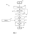
- Figure 1 shows a flow diagram of a method embodying the invention.
- the method shown generally at 100, starts at 102 and a mode of a timing unit is commenced at 104.
- time periods could be counted pending the occurrence of an event 108 caused by the timing unit.
- the value of the time interval between the commencement of the mode and the event is calculated 110 and compared 112 with a reference value 114; the result of the comparison is used to derive configuration data 116.
- the method ends at 118.
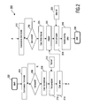
- FIG. 2 shows a flow diagram of a refined method embodying the invention.
- the method shown generally at 200, starts at 202 and a first mode of a timing unit is commenced at 204.
- time periods could be counted pending the occurrence of a first event 206 received from the timing unit.
- the value of a first time interval between the commencement of the first mode and the first event is calculated 208 and compared 210 with a first reference value 212; the result of the comparison enables an error value 214 to be calculated and optionally also the derivation of configuration data (not shown in Figure 2 ).
- the method continues where a second mode of the timing unit is commenced at 216.
- time periods could be counted pending the occurrence of a second event 218 received from the timing unit.
- the value of a second time interval between the commencement of the second mode and the second event is calculated 220. This calculated value is adjusted 222 using error value 214.
- the adjusted second time interval is then compared 224 with a second reference value 226; the result of the comparison is used to derive configuration data 228. The method ends at 230.
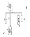
- FIG. 3 shows a schematic representation of an embodiment of a data processing apparatus.
- the data processing apparatus shown generally at 300, comprises a first port 302 operable to receive an event signal, a CPU 304, program ROM 306, RAM, 308 and a second port 312 operable to send a mode indication signal; all elements are interconnected by bus 310 according to any of the methods well known to the skilled person.
- the data processing apparatus may be integrated within a device such as a microprocessor or microcontroller; alternatively it may be a larger system wherein one or more elements is a separate entity.
- FIG. 4 shows a schematic representation of an embodiment of a data processing apparatus cooperating with a timing unit.
- the system shown generally at 400, comprises a timing unit 402 and a data processing apparatus 404.
- the data processing apparatus sends a mode indication signal 406 to the timing unit 402 which in response subsequently sends event signal 408 to the data processing apparatus.
- the timing unit sends an astable/periodic event signal
- the data processing apparatus may simply deduce the mode of the timing unit (e.g. using pre-stored data) and measure, as an example, the time interval between relevant event signals.
- FIG. 5 shows a schematic representation of a preferred embodiment of the invention comprising a microcontroller cooperating with a RC network timing unit.
- the system shown generally at 500, comprises a timing unit 502 (shown in dashed outline) connected by connections 506, 508 to a microcontroller 504.
- connections 506, 508 perform both mode indication signalling and event signalling as described in the following.
- the microcontroller 504 To prepare for a first (calibration) mode, the microcontroller 504 simultaneously grounds each end of capacitor 516 using lines 506, 508, thereby discharging capacitor 516.
- the first mode is signalled to the timing unit 502 by the microcontroller 504 releasing line 506 (whilst line 508 still grounds the lower end of capacitor 516) and making line 506 an input; the microcontroller also begins to count time periods, for example by incrementing an internal counter under software control.
- Capacitor 516 begins to charge via known and accurate resistance 514. Subsequently, at some level of voltage on the capacitor 516, the microcontroller will detect a logic 1 on line 506. The microcontroller will then stop incrementing the counter. The value of the counter is then compared with a stored value corresponding to that expected using the known resistance 514. The difference in the values mostly corresponds to the error due to the capacitor and various other tolerances within the microcontroller.
- the procedure is then repeated for another accurate resistance 512, which preferably is selected from a range of pre-determined values.
- the microcontroller 504 again simultaneously grounds each end of capacitor 516 using lines 506, 508, thereby discharging capacitor 516.
- the second mode is signalled to the timing unit 502 by the microcontroller 504 releasing line 508 (whilst line 506 grounds the upper end of capacitor 516) and making line 508 an input; the microcontroller again begins to count time periods, for example by incrementing an internal counter under software control.
- Capacitor 516 begins to charge via resistance 512. At some level of voltage on the capacitor 516, the microcontroller will detect a logic 1 on line 508. The microcontroller then stops incrementing the counter.
- the value of the counter is then adjusted using the error value calcu lated earlier, thereby compensating for the capacitor and microcontroller tolerance errors.
- the adjusted counter value is then compared with a range of reference values, preferably those corresponding to the range of pre-determined values for resistance 512 as described earlier. The closest match represents the configuration data denoted by the value of resistance 512.
- the method may allow a large set (range) of counter values (time intervals) to be resolved by the data processing apparatus in that the adjustment (compensation) reduces the error in the counter value obtained using the particular resistance 512.
- the calibration mode might also be used to derive some additional configuration data.
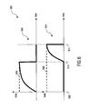
- Figure 6 shows a schematic representation depicting mode indication signals and event signals in relation to the embodiment of Figure 5 .
- Waveforms, shown generally at 600, of voltages at lines 506, 508 are shown at 602 and 604 respectively.
- the logic high detection voltage threshold of the microcontroller is at 606.
- the 'calibration mode' is depicted between 608 and 610.
- the 'derive configuration data mode' is depicted between 610 and 612.
- a method to obtain configuration data for a data processing apparatus by calculating 110 a time interval between the commencement of a mode 104 and a subsequent event 108.
- the calculated time interval is then compared 112 with one or more reference values 114.
- the result of the comparison is used to derive configuration data 116.
- the method may be further refined by including a calibration stage to reduce the error in the calculated time interval, thereby allowing comparison with a larger set of reference values 114, which in turn permits more configuration data to be derived from the calculated time interval.
Landscapes
- Engineering & Computer Science (AREA)
- Theoretical Computer Science (AREA)
- Quality & Reliability (AREA)
- Physics & Mathematics (AREA)
- General Engineering & Computer Science (AREA)
- General Physics & Mathematics (AREA)
- Debugging And Monitoring (AREA)
- Communication Control (AREA)
- Electric Clocks (AREA)
- Measurement Of Unknown Time Intervals (AREA)
- Test And Diagnosis Of Digital Computers (AREA)
- Complex Calculations (AREA)
- Arrangements For Transmission Of Measured Signals (AREA)
Applications Claiming Priority (3)
| Application Number | Priority Date | Filing Date | Title |
|---|---|---|---|
| GB0217708 | 2002-07-31 | ||
| GBGB0217708.7A GB0217708D0 (en) | 2002-07-31 | 2002-07-31 | Obtaining configuration data for a data processing apparatus |
| PCT/IB2003/003240 WO2004013754A2 (en) | 2002-07-31 | 2003-07-16 | Obtaining configuration data for a data processing apparatus |
Publications (2)
| Publication Number | Publication Date |
|---|---|
| EP1527389A2 EP1527389A2 (en) | 2005-05-04 |
| EP1527389B1 true EP1527389B1 (en) | 2011-10-05 |
Family
ID=9941430
Family Applications (1)
| Application Number | Title | Priority Date | Filing Date |
|---|---|---|---|
| EP03766547A Expired - Lifetime EP1527389B1 (en) | 2002-07-31 | 2003-07-16 | Obtaining configuration data for a data processing apparatus |
Country Status (8)
| Country | Link |
|---|---|
| US (1) | US7325153B2 (enExample) |
| EP (1) | EP1527389B1 (enExample) |
| JP (1) | JP2005535029A (enExample) |
| CN (1) | CN1672131B (enExample) |
| AT (1) | ATE527596T1 (enExample) |
| AU (1) | AU2003247079A1 (enExample) |
| GB (1) | GB0217708D0 (enExample) |
| WO (1) | WO2004013754A2 (enExample) |
Families Citing this family (6)
| Publication number | Priority date | Publication date | Assignee | Title |
|---|---|---|---|---|
| US7447655B2 (en) * | 2000-03-02 | 2008-11-04 | Trading Technologies International, Inc. | System and method for automatic scalping of a tradeable object in an electronic trading environment |
| DE102004030969A1 (de) * | 2004-06-26 | 2006-01-12 | Robert Bosch Gmbh | Verfahren und Vorrichtung zur Steuerung eines Bussystems sowie entsprechendes Bussystem |
| US7543173B2 (en) * | 2005-08-02 | 2009-06-02 | Hewlett-Packard Development Company, L.P. | Timestamp generator |
| US7631176B2 (en) * | 2006-07-24 | 2009-12-08 | Standard Microsystems Corporation | Resistor/capacitor based identification detection |
| US7719996B2 (en) * | 2006-09-25 | 2010-05-18 | Hewlett-Packard Development Company, L.P. | Encoding timestamps |
| FR3027402B1 (fr) * | 2014-10-21 | 2016-11-18 | Centre Nat Rech Scient | Circuit et procede pour le test sur puce d'une matrice de pixels |
Family Cites Families (6)
| Publication number | Priority date | Publication date | Assignee | Title |
|---|---|---|---|---|
| US3906346A (en) * | 1972-12-26 | 1975-09-16 | Us Navy | Precision time interval comparator |
| US5051622A (en) * | 1989-11-08 | 1991-09-24 | Chips And Technologies, Inc. | Power-on strap inputs |
| SE9002129D0 (sv) * | 1990-06-15 | 1990-06-15 | Siemens Elema Ab | Anordning foer stimulering av levande vaevnad |
| DE59108895D1 (de) * | 1991-12-18 | 1998-01-08 | Siemens Ag | Verfahren zur Uhrzeitführung in Computernetzen |
| JP3388053B2 (ja) * | 1995-03-20 | 2003-03-17 | 富士通株式会社 | データ収集システム用の伝送時間測定装置 |
| US5508650A (en) * | 1995-03-30 | 1996-04-16 | Maxim Integrated Products, Inc. | Dual feature input/timing pin |
-
2002
- 2002-07-31 GB GBGB0217708.7A patent/GB0217708D0/en not_active Ceased
-
2003
- 2003-07-16 AU AU2003247079A patent/AU2003247079A1/en not_active Abandoned
- 2003-07-16 WO PCT/IB2003/003240 patent/WO2004013754A2/en not_active Ceased
- 2003-07-16 EP EP03766547A patent/EP1527389B1/en not_active Expired - Lifetime
- 2003-07-16 CN CN03818218.1A patent/CN1672131B/zh not_active Expired - Fee Related
- 2003-07-16 AT AT03766547T patent/ATE527596T1/de not_active IP Right Cessation
- 2003-07-16 US US10/522,466 patent/US7325153B2/en not_active Expired - Lifetime
- 2003-07-16 JP JP2004525672A patent/JP2005535029A/ja not_active Ceased
Also Published As
| Publication number | Publication date |
|---|---|
| CN1672131A (zh) | 2005-09-21 |
| CN1672131B (zh) | 2012-05-23 |
| WO2004013754A3 (en) | 2004-12-29 |
| AU2003247079A1 (en) | 2004-02-23 |
| US7325153B2 (en) | 2008-01-29 |
| AU2003247079A8 (en) | 2004-02-23 |
| JP2005535029A (ja) | 2005-11-17 |
| WO2004013754A2 (en) | 2004-02-12 |
| US20060025982A1 (en) | 2006-02-02 |
| GB0217708D0 (en) | 2002-09-11 |
| ATE527596T1 (de) | 2011-10-15 |
| EP1527389A2 (en) | 2005-05-04 |
Similar Documents
| Publication | Publication Date | Title |
|---|---|---|
| EP1262755B1 (en) | Temperature sensing circuit and calibration method | |
| KR101771675B1 (ko) | 자동 정전용량형 터치 스캔 | |
| US8264231B2 (en) | Switch circuit | |
| JPH10503882A (ja) | インテリジェントなバッテリ管理を行うためのアナログ前置回路を備えるマイクロコントローラ | |
| JPH10508460A (ja) | オンチップアナログ要素のディジタル微調整 | |
| EP1527389B1 (en) | Obtaining configuration data for a data processing apparatus | |
| RU2324286C1 (ru) | Устройство для аналого-цифрового преобразования измеренного напряжения | |
| US6098142A (en) | Apparatus and method for using a communications port in polling mode and without interrupts | |
| CN108663070A (zh) | 数字传感器系统 | |
| CN101097494A (zh) | 具有自动校准提示功能的触控屏幕装置及其方法 | |
| US4783747A (en) | Control device for an automatic vending machine | |
| US20030047360A1 (en) | Position detector and position indicator therefor | |
| CN113390452A (zh) | 一种开关型仪表校准方法及装置 | |
| KR101000259B1 (ko) | 정전압부를 가진 자동차용 전압 분배형 스위치 입력 회로 및 방법 | |
| CN112504519B (zh) | 一种压力检测电路、装置及压力输入装置 | |
| JPH0217415A (ja) | インクリメント型発信器の信号の評価方法および装置 | |
| CN112674897A (zh) | 压力数据处理控制方法、控制系统及计算机可读存储介质 | |
| JPS5952325A (ja) | 停電・復電検知集積回路 | |
| US9797936B2 (en) | Counter enhancements for improved performance and ease-of-use | |
| US7183869B2 (en) | Circuit and method for temperature compensation | |
| JPH07102275B2 (ja) | 洗濯機の運転制御装置 | |
| JPS62249311A (ja) | スイツチの機能選択方式 | |
| JPS5952324A (ja) | 停電・復電検知回路 | |
| CN120971932A (zh) | 一种pwm诊断电路、pwm诊断方法以及电子设备 | |
| KR0149869B1 (ko) | 전자기기의 센서값 정밀 감지장치 |
Legal Events
| Date | Code | Title | Description |
|---|---|---|---|
| PUAI | Public reference made under article 153(3) epc to a published international application that has entered the european phase |
Free format text: ORIGINAL CODE: 0009012 |
|
| AK | Designated contracting states |
Kind code of ref document: A2 Designated state(s): AT BE BG CH CY CZ DE DK EE ES FI FR GB GR HU IE IT LI LU MC NL PT RO SE SI SK TR |
|
| AX | Request for extension of the european patent |
Extension state: AL LT LV MK |
|
| 17P | Request for examination filed |
Effective date: 20050629 |
|
| RBV | Designated contracting states (corrected) |
Designated state(s): AT BE BG CH CY CZ DE DK EE ES FI FR GB GR HU IE IT LI LU MC NL PT RO SE SI SK TR |
|
| DAX | Request for extension of the european patent (deleted) | ||
| 17Q | First examination report despatched |
Effective date: 20061102 |
|
| RAP1 | Party data changed (applicant data changed or rights of an application transferred) |
Owner name: NXP B.V. |
|
| GRAP | Despatch of communication of intention to grant a patent |
Free format text: ORIGINAL CODE: EPIDOSNIGR1 |
|
| GRAS | Grant fee paid |
Free format text: ORIGINAL CODE: EPIDOSNIGR3 |
|
| GRAA | (expected) grant |
Free format text: ORIGINAL CODE: 0009210 |
|
| AK | Designated contracting states |
Kind code of ref document: B1 Designated state(s): AT BE BG CH CY CZ DE DK EE ES FI FR GB GR HU IE IT LI LU MC NL PT RO SE SI SK TR |
|
| REG | Reference to a national code |
Ref country code: GB Ref legal event code: FG4D |
|
| REG | Reference to a national code |
Ref country code: CH Ref legal event code: EP |
|
| REG | Reference to a national code |
Ref country code: DE Ref legal event code: R081 Ref document number: 60338652 Country of ref document: DE Owner name: LLL HOLDINGS 6, LLC, WILMINGTON, US Free format text: FORMER OWNER: KONINKLIJKE PHILIPS ELECTRONICS N.V., EINDHOVEN, NL Ref country code: DE Ref legal event code: R081 Ref document number: 60338652 Country of ref document: DE Owner name: III HOLDINGS 6, LLC, WILMINGTON, US Free format text: FORMER OWNER: KONINKLIJKE PHILIPS ELECTRONICS N.V., EINDHOVEN, NL |
|
| REG | Reference to a national code |
Ref country code: IE Ref legal event code: FG4D |
|
| REG | Reference to a national code |
Ref country code: DE Ref legal event code: R096 Ref document number: 60338652 Country of ref document: DE Effective date: 20111215 |
|
| REG | Reference to a national code |
Ref country code: NL Ref legal event code: VDEP Effective date: 20111005 |
|
| PG25 | Lapsed in a contracting state [announced via postgrant information from national office to epo] |
Ref country code: SI Free format text: LAPSE BECAUSE OF FAILURE TO SUBMIT A TRANSLATION OF THE DESCRIPTION OR TO PAY THE FEE WITHIN THE PRESCRIBED TIME-LIMIT Effective date: 20111005 |
|
| REG | Reference to a national code |
Ref country code: AT Ref legal event code: MK05 Ref document number: 527596 Country of ref document: AT Kind code of ref document: T Effective date: 20111005 |
|
| PG25 | Lapsed in a contracting state [announced via postgrant information from national office to epo] |
Ref country code: BE Free format text: LAPSE BECAUSE OF FAILURE TO SUBMIT A TRANSLATION OF THE DESCRIPTION OR TO PAY THE FEE WITHIN THE PRESCRIBED TIME-LIMIT Effective date: 20111005 |
|
| PG25 | Lapsed in a contracting state [announced via postgrant information from national office to epo] |
Ref country code: GR Free format text: LAPSE BECAUSE OF FAILURE TO SUBMIT A TRANSLATION OF THE DESCRIPTION OR TO PAY THE FEE WITHIN THE PRESCRIBED TIME-LIMIT Effective date: 20120106 Ref country code: SE Free format text: LAPSE BECAUSE OF FAILURE TO SUBMIT A TRANSLATION OF THE DESCRIPTION OR TO PAY THE FEE WITHIN THE PRESCRIBED TIME-LIMIT Effective date: 20111005 Ref country code: NL Free format text: LAPSE BECAUSE OF FAILURE TO SUBMIT A TRANSLATION OF THE DESCRIPTION OR TO PAY THE FEE WITHIN THE PRESCRIBED TIME-LIMIT Effective date: 20111005 Ref country code: PT Free format text: LAPSE BECAUSE OF FAILURE TO SUBMIT A TRANSLATION OF THE DESCRIPTION OR TO PAY THE FEE WITHIN THE PRESCRIBED TIME-LIMIT Effective date: 20120206 |
|
| PG25 | Lapsed in a contracting state [announced via postgrant information from national office to epo] |
Ref country code: CY Free format text: LAPSE BECAUSE OF FAILURE TO SUBMIT A TRANSLATION OF THE DESCRIPTION OR TO PAY THE FEE WITHIN THE PRESCRIBED TIME-LIMIT Effective date: 20111005 |
|
| PG25 | Lapsed in a contracting state [announced via postgrant information from national office to epo] |
Ref country code: DK Free format text: LAPSE BECAUSE OF FAILURE TO SUBMIT A TRANSLATION OF THE DESCRIPTION OR TO PAY THE FEE WITHIN THE PRESCRIBED TIME-LIMIT Effective date: 20111005 Ref country code: CZ Free format text: LAPSE BECAUSE OF FAILURE TO SUBMIT A TRANSLATION OF THE DESCRIPTION OR TO PAY THE FEE WITHIN THE PRESCRIBED TIME-LIMIT Effective date: 20111005 Ref country code: SK Free format text: LAPSE BECAUSE OF FAILURE TO SUBMIT A TRANSLATION OF THE DESCRIPTION OR TO PAY THE FEE WITHIN THE PRESCRIBED TIME-LIMIT Effective date: 20111005 Ref country code: EE Free format text: LAPSE BECAUSE OF FAILURE TO SUBMIT A TRANSLATION OF THE DESCRIPTION OR TO PAY THE FEE WITHIN THE PRESCRIBED TIME-LIMIT Effective date: 20111005 Ref country code: BG Free format text: LAPSE BECAUSE OF FAILURE TO SUBMIT A TRANSLATION OF THE DESCRIPTION OR TO PAY THE FEE WITHIN THE PRESCRIBED TIME-LIMIT Effective date: 20120105 |
|
| PLBE | No opposition filed within time limit |
Free format text: ORIGINAL CODE: 0009261 |
|
| STAA | Information on the status of an ep patent application or granted ep patent |
Free format text: STATUS: NO OPPOSITION FILED WITHIN TIME LIMIT |
|
| PG25 | Lapsed in a contracting state [announced via postgrant information from national office to epo] |
Ref country code: RO Free format text: LAPSE BECAUSE OF FAILURE TO SUBMIT A TRANSLATION OF THE DESCRIPTION OR TO PAY THE FEE WITHIN THE PRESCRIBED TIME-LIMIT Effective date: 20111005 Ref country code: IT Free format text: LAPSE BECAUSE OF FAILURE TO SUBMIT A TRANSLATION OF THE DESCRIPTION OR TO PAY THE FEE WITHIN THE PRESCRIBED TIME-LIMIT Effective date: 20111005 |
|
| PGFP | Annual fee paid to national office [announced via postgrant information from national office to epo] |
Ref country code: GB Payment date: 20120629 Year of fee payment: 10 |
|
| 26N | No opposition filed |
Effective date: 20120706 |
|
| REG | Reference to a national code |
Ref country code: DE Ref legal event code: R097 Ref document number: 60338652 Country of ref document: DE Effective date: 20120706 |
|
| PG25 | Lapsed in a contracting state [announced via postgrant information from national office to epo] |
Ref country code: AT Free format text: LAPSE BECAUSE OF FAILURE TO SUBMIT A TRANSLATION OF THE DESCRIPTION OR TO PAY THE FEE WITHIN THE PRESCRIBED TIME-LIMIT Effective date: 20111005 |
|
| PG25 | Lapsed in a contracting state [announced via postgrant information from national office to epo] |
Ref country code: MC Free format text: LAPSE BECAUSE OF NON-PAYMENT OF DUE FEES Effective date: 20120731 |
|
| REG | Reference to a national code |
Ref country code: CH Ref legal event code: PL |
|
| PG25 | Lapsed in a contracting state [announced via postgrant information from national office to epo] |
Ref country code: LI Free format text: LAPSE BECAUSE OF NON-PAYMENT OF DUE FEES Effective date: 20120731 Ref country code: CH Free format text: LAPSE BECAUSE OF NON-PAYMENT OF DUE FEES Effective date: 20120731 Ref country code: ES Free format text: LAPSE BECAUSE OF FAILURE TO SUBMIT A TRANSLATION OF THE DESCRIPTION OR TO PAY THE FEE WITHIN THE PRESCRIBED TIME-LIMIT Effective date: 20120116 |
|
| REG | Reference to a national code |
Ref country code: IE Ref legal event code: MM4A |
|
| PG25 | Lapsed in a contracting state [announced via postgrant information from national office to epo] |
Ref country code: FI Free format text: LAPSE BECAUSE OF FAILURE TO SUBMIT A TRANSLATION OF THE DESCRIPTION OR TO PAY THE FEE WITHIN THE PRESCRIBED TIME-LIMIT Effective date: 20111005 |
|
| REG | Reference to a national code |
Ref country code: GB Ref legal event code: 732E Free format text: REGISTERED BETWEEN 20130606 AND 20130612 |
|
| PG25 | Lapsed in a contracting state [announced via postgrant information from national office to epo] |
Ref country code: IE Free format text: LAPSE BECAUSE OF NON-PAYMENT OF DUE FEES Effective date: 20120716 |
|
| GBPC | Gb: european patent ceased through non-payment of renewal fee |
Effective date: 20130716 |
|
| PG25 | Lapsed in a contracting state [announced via postgrant information from national office to epo] |
Ref country code: TR Free format text: LAPSE BECAUSE OF FAILURE TO SUBMIT A TRANSLATION OF THE DESCRIPTION OR TO PAY THE FEE WITHIN THE PRESCRIBED TIME-LIMIT Effective date: 20111005 Ref country code: GB Free format text: LAPSE BECAUSE OF NON-PAYMENT OF DUE FEES Effective date: 20130716 |
|
| PG25 | Lapsed in a contracting state [announced via postgrant information from national office to epo] |
Ref country code: LU Free format text: LAPSE BECAUSE OF NON-PAYMENT OF DUE FEES Effective date: 20120716 |
|
| PG25 | Lapsed in a contracting state [announced via postgrant information from national office to epo] |
Ref country code: HU Free format text: LAPSE BECAUSE OF FAILURE TO SUBMIT A TRANSLATION OF THE DESCRIPTION OR TO PAY THE FEE WITHIN THE PRESCRIBED TIME-LIMIT Effective date: 20030716 |
|
| REG | Reference to a national code |
Ref country code: DE Ref legal event code: R084 Ref document number: 60338652 Country of ref document: DE |
|
| REG | Reference to a national code |
Ref country code: DE Ref legal event code: R084 Ref document number: 60338652 Country of ref document: DE Effective date: 20141015 |
|
| REG | Reference to a national code |
Ref country code: FR Ref legal event code: PLFP Year of fee payment: 13 |
|
| REG | Reference to a national code |
Ref country code: DE Ref legal event code: R081 Ref document number: 60338652 Country of ref document: DE Owner name: LLL HOLDINGS 6, LLC, WILMINGTON, US Free format text: FORMER OWNER: NXP B.V., EINDHOVEN, NL Ref country code: DE Ref legal event code: R081 Ref document number: 60338652 Country of ref document: DE Owner name: III HOLDINGS 6, LLC, WILMINGTON, US Free format text: FORMER OWNER: NXP B.V., EINDHOVEN, NL |
|
| REG | Reference to a national code |
Ref country code: FR Ref legal event code: TP Owner name: III HOLDINGS 6, LLC, US Effective date: 20160118 |
|
| REG | Reference to a national code |
Ref country code: FR Ref legal event code: PLFP Year of fee payment: 14 |
|
| REG | Reference to a national code |
Ref country code: FR Ref legal event code: PLFP Year of fee payment: 15 |
|
| PGFP | Annual fee paid to national office [announced via postgrant information from national office to epo] |
Ref country code: FR Payment date: 20170621 Year of fee payment: 15 |
|
| REG | Reference to a national code |
Ref country code: DE Ref legal event code: R082 Ref document number: 60338652 Country of ref document: DE Representative=s name: MUELLER-BORE & PARTNER PATENTANWAELTE PARTG MB, DE Ref country code: DE Ref legal event code: R081 Ref document number: 60338652 Country of ref document: DE Owner name: III HOLDINGS 6, LLC, WILMINGTON, US Free format text: FORMER OWNER: LLL HOLDINGS 6, LLC, WILMINGTON, DEL., US |
|
| PGFP | Annual fee paid to national office [announced via postgrant information from national office to epo] |
Ref country code: DE Payment date: 20170726 Year of fee payment: 15 |
|
| REG | Reference to a national code |
Ref country code: DE Ref legal event code: R119 Ref document number: 60338652 Country of ref document: DE |
|
| PG25 | Lapsed in a contracting state [announced via postgrant information from national office to epo] |
Ref country code: DE Free format text: LAPSE BECAUSE OF NON-PAYMENT OF DUE FEES Effective date: 20190201 Ref country code: FR Free format text: LAPSE BECAUSE OF NON-PAYMENT OF DUE FEES Effective date: 20180731 |