EP1526763A1 - Steuerungsschaltung für eine elektronische Hochdruckentladungslampe - Google Patents
Steuerungsschaltung für eine elektronische Hochdruckentladungslampe Download PDFInfo
- Publication number
- EP1526763A1 EP1526763A1 EP04024298A EP04024298A EP1526763A1 EP 1526763 A1 EP1526763 A1 EP 1526763A1 EP 04024298 A EP04024298 A EP 04024298A EP 04024298 A EP04024298 A EP 04024298A EP 1526763 A1 EP1526763 A1 EP 1526763A1
- Authority
- EP
- European Patent Office
- Prior art keywords
- hid
- driver
- circuit
- lamp
- power
- Prior art date
- Legal status (The legal status is an assumption and is not a legal conclusion. Google has not performed a legal analysis and makes no representation as to the accuracy of the status listed.)
- Granted
Links
- 229910001507 metal halide Inorganic materials 0.000 claims abstract description 9
- 150000005309 metal halides Chemical class 0.000 claims abstract description 9
- DGAQECJNVWCQMB-PUAWFVPOSA-M Ilexoside XXIX Chemical compound C[C@@H]1CC[C@@]2(CC[C@@]3(C(=CC[C@H]4[C@]3(CC[C@@H]5[C@@]4(CC[C@@H](C5(C)C)OS(=O)(=O)[O-])C)C)[C@@H]2[C@]1(C)O)C)C(=O)O[C@H]6[C@@H]([C@H]([C@@H]([C@H](O6)CO)O)O)O.[Na+] DGAQECJNVWCQMB-PUAWFVPOSA-M 0.000 claims abstract description 8
- 229910052708 sodium Inorganic materials 0.000 claims abstract description 8
- 239000011734 sodium Substances 0.000 claims abstract description 8
- 230000001052 transient effect Effects 0.000 claims abstract description 5
- 239000003990 capacitor Substances 0.000 claims description 47
- 238000012937 correction Methods 0.000 claims description 8
- 238000001914 filtration Methods 0.000 claims description 8
- 238000010586 diagram Methods 0.000 description 38
- 238000000034 method Methods 0.000 description 22
- 238000013461 design Methods 0.000 description 16
- 230000003321 amplification Effects 0.000 description 6
- 238000003199 nucleic acid amplification method Methods 0.000 description 6
- 230000002093 peripheral effect Effects 0.000 description 5
- 238000005070 sampling Methods 0.000 description 5
- 230000006641 stabilisation Effects 0.000 description 5
- 238000011105 stabilization Methods 0.000 description 5
- 230000001143 conditioned effect Effects 0.000 description 4
- 230000001419 dependent effect Effects 0.000 description 4
- 238000007537 lampworking Methods 0.000 description 4
- 230000010355 oscillation Effects 0.000 description 4
- 230000008569 process Effects 0.000 description 3
- 230000001960 triggered effect Effects 0.000 description 3
- XEEYBQQBJWHFJM-UHFFFAOYSA-N Iron Chemical group [Fe] XEEYBQQBJWHFJM-UHFFFAOYSA-N 0.000 description 2
- 241001125929 Trisopterus luscus Species 0.000 description 2
- 230000002159 abnormal effect Effects 0.000 description 2
- 230000033228 biological regulation Effects 0.000 description 2
- 230000005540 biological transmission Effects 0.000 description 2
- 230000003247 decreasing effect Effects 0.000 description 2
- 239000006185 dispersion Substances 0.000 description 2
- 230000007246 mechanism Effects 0.000 description 2
- 238000012986 modification Methods 0.000 description 2
- 230000004048 modification Effects 0.000 description 2
- UXUFTKZYJYGMGO-CMCWBKRRSA-N (2s,3s,4r,5r)-5-[6-amino-2-[2-[4-[3-(2-aminoethylamino)-3-oxopropyl]phenyl]ethylamino]purin-9-yl]-n-ethyl-3,4-dihydroxyoxolane-2-carboxamide Chemical compound O[C@@H]1[C@H](O)[C@@H](C(=O)NCC)O[C@H]1N1C2=NC(NCCC=3C=CC(CCC(=O)NCCN)=CC=3)=NC(N)=C2N=C1 UXUFTKZYJYGMGO-CMCWBKRRSA-N 0.000 description 1
- 101100432968 Mus musculus Yrdc gene Proteins 0.000 description 1
- XUIMIQQOPSSXEZ-UHFFFAOYSA-N Silicon Chemical compound [Si] XUIMIQQOPSSXEZ-UHFFFAOYSA-N 0.000 description 1
- 230000004913 activation Effects 0.000 description 1
- 230000002457 bidirectional effect Effects 0.000 description 1
- 230000003750 conditioning effect Effects 0.000 description 1
- 238000010276 construction Methods 0.000 description 1
- 238000007599 discharging Methods 0.000 description 1
- 230000000694 effects Effects 0.000 description 1
- -1 for example Substances 0.000 description 1
- 150000004820 halides Chemical class 0.000 description 1
- 150000002500 ions Chemical class 0.000 description 1
- 238000004519 manufacturing process Methods 0.000 description 1
- 239000000463 material Substances 0.000 description 1
- 235000012054 meals Nutrition 0.000 description 1
- 238000010606 normalization Methods 0.000 description 1
- 238000005457 optimization Methods 0.000 description 1
- 230000002035 prolonged effect Effects 0.000 description 1
- 238000011160 research Methods 0.000 description 1
- 229910052710 silicon Inorganic materials 0.000 description 1
- 239000010703 silicon Substances 0.000 description 1
- 239000007858 starting material Substances 0.000 description 1
- 230000001629 suppression Effects 0.000 description 1
Images










Classifications
-
- H—ELECTRICITY
- H05—ELECTRIC TECHNIQUES NOT OTHERWISE PROVIDED FOR
- H05B—ELECTRIC HEATING; ELECTRIC LIGHT SOURCES NOT OTHERWISE PROVIDED FOR; CIRCUIT ARRANGEMENTS FOR ELECTRIC LIGHT SOURCES, IN GENERAL
- H05B41/00—Circuit arrangements or apparatus for igniting or operating discharge lamps
- H05B41/14—Circuit arrangements
- H05B41/26—Circuit arrangements in which the lamp is fed by power derived from DC by means of a converter, e.g. by high-voltage DC
- H05B41/28—Circuit arrangements in which the lamp is fed by power derived from DC by means of a converter, e.g. by high-voltage DC using static converters
- H05B41/288—Circuit arrangements in which the lamp is fed by power derived from DC by means of a converter, e.g. by high-voltage DC using static converters with semiconductor devices and specially adapted for lamps without preheating electrodes, e.g. for high-intensity discharge lamps, high-pressure mercury or sodium lamps or low-pressure sodium lamps
- H05B41/292—Arrangements for protecting lamps or circuits against abnormal operating conditions
- H05B41/2921—Arrangements for protecting lamps or circuits against abnormal operating conditions for protecting the circuit against abnormal operating conditions
- H05B41/2926—Arrangements for protecting lamps or circuits against abnormal operating conditions for protecting the circuit against abnormal operating conditions against internal abnormal circuit conditions
-
- Y—GENERAL TAGGING OF NEW TECHNOLOGICAL DEVELOPMENTS; GENERAL TAGGING OF CROSS-SECTIONAL TECHNOLOGIES SPANNING OVER SEVERAL SECTIONS OF THE IPC; TECHNICAL SUBJECTS COVERED BY FORMER USPC CROSS-REFERENCE ART COLLECTIONS [XRACs] AND DIGESTS
- Y02—TECHNOLOGIES OR APPLICATIONS FOR MITIGATION OR ADAPTATION AGAINST CLIMATE CHANGE
- Y02B—CLIMATE CHANGE MITIGATION TECHNOLOGIES RELATED TO BUILDINGS, e.g. HOUSING, HOUSE APPLIANCES OR RELATED END-USER APPLICATIONS
- Y02B20/00—Energy efficient lighting technologies, e.g. halogen lamps or gas discharge lamps
Definitions
- the invention relates in general to a ballast of a high intensity discharge (HID) lamp driver. More particularly, the invention relates to a high-efficiency electronic ballast with wide input voltage range, high power factor, low current total harmonic distortion (THD) and low current crest factor.
- HID high intensity discharge
- TDD low current total harmonic distortion
- the HID ballast is an important component of a HID lamp.
- the performance of the ballast directly affects the starting, the color temperature, the life period and the working stability of the HID lamp.
- the electronic HID ballast can overcome the disadvantages caused by the iron core HID ballast.
- the ratio of the loading power transmission to the weight of the ballast is high, and the ratio of the power consumption to the controlled power is low.
- the disadvantages of the electronic HID ballast are that the starting of the electronic HID ballast is complex, the power control and the circuit protection are hard to design.
- a conventional basic switching power supply can be classified into three types, one is a flyback and forward converter switching power supply, another is a push-pull switching power supply, and the other is a half bridge/full bridge switching power supply.
- the power loading of the flyback and forward converter switching power supply is small, and the duty cycle is only about 0.4.
- the use of the flyback and forward converter switching power supply in a HID ballast is described, for example, in the paper of E. Deng and S. Cuk, Single Stage High Power Factor Lamp Ballast, APEC'94, p.441-449, 1994, wherein an electronic HID ballast used in a low power metal halide (MHL) is described.
- MHL low power metal halide
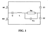
- FIG. 1 is a circuit diagram illustrating a conventional electronic HID ballast using a half bridge/full bridge switching power supply.
- an electronic HID ballast can drive the HID lamp in a high frequency range. Before the lamp is turned on, a voltage less than a maximum permissible voltage is provided to the lamp, wherein a pulse voltage is added to the voltage.
- an open-circuit voltage of the electronic HID ballast has a quasi-square waveform with an over-pulse peak, and the voltage is used as a trigger pulse.
- FIG. 2 is a waveform diagram illustrating a quasi-square wave having an over-pulse peak as a trigger pulse of the HID lamp. It is noted that different lamp with different type and power has different quasi-square wave with different amplitude and width.
- the limitation of the HID lamp is that a higher cold-start voltage is required but after lamp is turned on, the hot lamp can not be started again in order to protect the lamp. Therefore, in order to make sure that the lamp can be turned on, a higher amplitude and a wider width of the pulse voltage is preferable. But in order to prolong the operating life of the lamp, the amplitude of the voltage is preferably as low as possible.
- the pulse voltage U can be expanded by a Fourier series as illustrated in the following equation (1):
- the circuit shown in FIG. I 1 may be regarded as an open circuit.
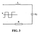
- the circuit can be simulated by a serial connected circuit RLC as shown in FIG. 3 (wherein R is calculated from the power loss of the circuit).
- the circuit can be solved by the following equation (2): or When the damped oscillation is considered only, the current I can be expanded by the following equation (4):
- the loop of the circuit is designed a little far away from the resonance point of the circuit in order to prevent the Vmax from damaging the circuit by adjusting the capacitance Cj.
- the above circuit as shown in FIG. 1 is used as an electronic HID ballast.
- the lamp may be damaged suddenly due to the over-pulse peak of the voltage.
- the voltage Vmax is about 1.2 kV.
- Imax is about 15A if ⁇ L is about 80.
- Imax is larger than about 20A. Therefore, at the instance of the starting of the lamp, the high current may damage the lamp. If the starting fails, the over-pulse peak voltage will destroy the loop of the circuit or the lamp. Therefore, to provide the circuit shown in FIG. 1 as an electronic ballast of the HID lamp is not practical.
- the provided circuit is not in the basic resonance, for example, the resonance is in 3 rd order or 5 th order, the resonance current can be reduced. But the parameters of the circuit need to be adjusted to match the 3 rd or the 5 th order resonance condition.
- the adjustments of the parameters are dependent on the whole circuits and need to be optimized by try and error method. Moreover, the power consumption of the circuit will increased since it is proportional to the order of the resonance. Accordingly, the peak value of the voltage will reduce, and thus the opportunity of failure of the startup will increase.
- FIG. 4 is a circuit diagram illustrating a conventional startup circuits for triggering the HID lamp of 4 times of voltage type.
- the circuit of FIG. 4 is provided as a iron core ballast or a so-called hot starter.
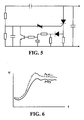
- FIG. 5 is a circuit diagram illustrating another conventional startup circuits for trigger the HID lamp. Referring to FIG. 5, however, the stability of the circuit and the operating life of the components of the circuit are also the issues of the circuit.
- the voltage curve from the startup to the stable working period of a conventional HID lamp is shown in FIG. 6.
- the current of the lamp After the voltage of the lamp reach the working voltage, the current of the lamp must be stabilized at the working current; and the current in each period must be continuously.
- two sub-zero voltages can not be occurred to prevent turning off of the arc of the lamp.
- the waveform of the voltage of the lamp is a sine wave, quasi-sine wave, square wave, quasi-square wave, and no matter what the waveform of the current of the lamp is a sine wave, square wave, saw wave or even a sharp peak wave
- the wave peak coefficient should less than 1.8 times of that of the sharp peak wave.
- the sound resonance issue is a special characteristic of the HID lamp.
- the sound resonance is caused by the standing wave formed by the superposition of the pressure waves reflected from the lamp tube, wherein the pressure wave is caused by the transmission of the high frequency electrical power in the ion plasma of discharged by the arc of the lamp. Therefore, the arc of the lamp will be influenced by the pressure wave of the sound resonance, and thus the arc and the voltage of the lamp will be unstable. Therefore, the light emitted from the arc of the lamp will flicker, more particularly, the arc of the lamp will be distorted or destroyed, and thus the lamp will be burned out or even the lamp tube will be blown up.
- the first method is to operate the lamp in a frequency range far away from the sound resonance frequency.
- the second method is to add one or more proper low frequency component before the sound resonance occurs to prevent from generating of the sound resonance.
- the third method is to eliminate the band of frequency of the current of the lamp near the band of frequency of the sound resonance. Accordingly, a preferable method is to add one or more low frequency component to the high frequency current, or to turn on the lamp by using a DC current. Moreover, an external startup circuit and a corresponding protection circuit are also required in the methods described above.
- the HID lamp with different type and different working power has their own stable working frequency band. If the frequency band is not suitable for the lamp, the sound resonance may occur, the arc may flicker, and in some specific frequency bands, the tube may burn out. Therefore, in order to operate the HID lamp in a stable high frequency working condition, the frequency band must be selected according to the type, the working power, the shape, and the gas pressure of the lamp. Moreover, the HID tube pressure has a specific dispersion characteristic, and the working power and the color temperature of the lamp will be effected by the dispersion characteristic. Therefore, the working power must be effectively controlled by the circuit of the ballast. Moreover, the harmonics of the input current of the HID electronic ballast will damage the HID lamp.
- FIG. 7 is the block diagram illustrating the circuit of MC34262 of Motorola
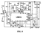
- FIG. 8 is the block diagram illustrating the circuit of L4981 A of ST
- FIG. 7 is the block diagram illustrating the circuit of MC34262 of Motorola
- FIG. 8 is the block diagram illustrating the circuit of L4981 A of ST
- FIG. 8 is the block diagram illustrating the circuit of L4981 A of ST
- FIG. 9 is the block diagram illustrating the UCC3817 of Texas Instrument (TI).
- the MC34262 is worked in a range of 185V to 265V/250W, but it is difficult to work in a range of 85V to 265 V/250 W. Therefore, ST developed the L4981A (shown in FIG. 8), wherein the IC can work in a range of 88V to 264V/200W.
- TI developed the UCC3817 (shown in FIG. 9), wherein the dynamic range of the IC is in a range of about 85V to about 270V.
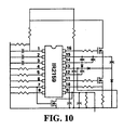
- FIG. 10 is the block diagram illustrating the circuit of L2155, L2156 or L2159 of IR
- FIG. 11 is the block diagram illustrating the circuit of UCC3580 or 3895 of TI.
- These ICs can only be provided in a limited range of loading power. If the circuit peripheral to these ICs is modified to fit the HID lamp, the cost and the complexity of the circuits will increase. If other simple IC circuit, for example, the one shown in Fig. 12, is used to drive a lamp with power loading of 250W to 400W or even 1000W, the lamp and the IC will often be blown up on starting the lamp.
- the circuit using the self-excited oscillation method can also be employed for enhancement of the driving power instead of using the ICs.
- the loading power of the circuit is also limited in a range, for example, below 150W.
- the loading power can be enhanced by using the method of increasing the area of the magnetic core, the stabilization of the power is still an issue. For example, if the power loading of the circuit is 150W, in general, the power will drop during the operation and finally maintain at about 120W.
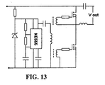
- FIG. 13 is a block diagram illustrating another circuit of a conventional power drive circuit. It is noted that more than one inductor is provided in the circuit of FIG. 13. Accordingly, except for the stabilization of the power, the complexity and cost of the circuit are also another issue of the circuit.
- Another method to enhance the driving power is to replace the power amplifier from the half bridge inverter to a full bridge inverter, and hence, the primary circuit needs to be changed according to the secondary circuit.
- a method of using capacitor as the voltage divider to enhance the power can also be provided instead of changing the half-bridge inverter, or even changing the electronic component of the current limit inductor.
- the lamp should not be started.
- the ballast and the lamp are not protected by a protection circuit, the ballast will apply high voltage pulses to try to start the lamp when any one of the problem occurs.
- the ballast and the lamp will be damaged, the power consumption will increase, and the electromagnetic interference will also increased. Therefore, a protection circuit for the ballast and the lamp is required.
- FIG. 14 is a block diagram illustrating a conventional protection circuit. Referring to FIG. 14, a voltage signal proportional to the resonance voltage is provided through the assistant coil of the current limit inductor. The voltage signal is filtered and rectified to be a DC sampling voltage, the DC sampling voltage is then divided and applied to the base-emitter of the protection transistor 1402. The collector of the transistor 1402 is connected to the triggering pole (leg 2) of the timing IC NE555.
- the IC NE555 is connected in a single stable state, the leg 6 and leg 7 of NE555 is connected to the timer RC, the output pole (leg 3) is connected to the enabling pole (leg 5) of power driving IC (CD4046).
- CD4046 power driving IC
- a low voltage level is applied to the leg 5 of CD4046, CD4046 is normally operated, but when a high voltage level is applied to the leg 5 of CD4046, CD4046 is off. Accordingly, when a low level DC sampling voltage is applied to the transistor 1402, the transistor 1402 is off and NE555 is not triggered, a low voltage level is applied to the leg 3 of CD4046, thus CD4046 is normally operated.
- the protection time of the circuit is determined by the timer RC, in general, the protection time is set about 5 minutes in order to restart the lamp.
- the IC 2159 or IC 2156 of IR company can also be provided as the protection circuit.
- a variety of the conventional protection circuit can not be directly provided as a protection circuit, but must be modified and incorporated with another external circuit to fit the protection requirement. Therefore, the cost and the complexity of the protection circuit is increased.
- an electronic ballast for HID lamp at least including the power amplification, light adjusting, restarting, timing and protection circuits is required.
- the present invention is to provide an electronic HID ballast for a HID lamp for a low power to middle and high power input to solve the problems generated in the conventional design of the ballast.
- a high intensity discharge (HID) driver for a HID lamp which can be used as a HID ballast.
- the HID driver at least includes an input processor connected to an input power for suppressing a transient and an in-rush current of the input power, a main driver connected to the input processor and a HID lamp for driving and amplifying the input power; and a protection circuit connected to the main driver and the HID lamp for controlling the timing of starting after a failure condition.
- the HID driver can be applied to a high pressure sodium (HPS) lamp or a metal halide lamp (HML).
- HPS high pressure sodium
- HML metal halide lamp
- the input power is an alternating current (AC) voltage in a range of about 85V to about 305V at 50HZ/60Hz.
- AC alternating current
- the HID driver may further include a timing circuit connected to the main driver for controlling a timing, and a starting circuit connected to the timing circuit and the HID lamp for starting the HID lamp.
- the input power is an AC voltage in a range of about 85V to about 305V at 50HZ/60Hz.
- the input processor further includes an rectifier and filter circuit.
- the input processor further includes an electromagnetic wave controller (EMC) for suppressing an electromagnetic wave interference.
- EMC electromagnetic wave controller
- NTC negative temperature control
- the input processor further includes a voltage sensitive resistor (RV) for suppressing the in-rush current.
- the rectifier and filter circuit comprises a diode bridge circuit.
- the main driver further includes a power factor correction (PFC) circuit connected to the input processor and the protection circuit.
- the main driver further comprises a special power supply connected to the input processor, the PFC circuit, the timing circuit and the protection circuit.
- the special power supply comprises at least two circuit paths for supplying power.
- the main driver further comprises a power driver connected to the input processor, the special power supply, the PFC circuit and the protection circuit.
- the power driver further comprises a light adjuster for adjusting the brightness of the HID lamp by adjusting a frequency of the power driver.
- the main driver further comprises a half-bridge inverter connected to the input processor and the HID lamp.
- the main driver further comprises a half bridge inverter connected to the input processor and the HID lamp.
- the main driver further comprises a feedback control circuit connected to the PFC circuit, the power drive and the half bridge inverter.
- the starting circuit comprises a sub-starting circuit having a SIDAC connected in series to a diode and an inductor for starting the HID lamp quickly and reliably.
- the starting circuit comprises a capacitor connected in parallel to the HID lamp in replacement of the sub-starting circuit when the HID lamp is a metal halide lamp (HML).
- HML metal halide lamp
- the starting circuit comprises a circuit having a capacitor for fine tuning an output of the HID lamp, a brightness of the HID lamp, and a low-frequency content for controlling an induced sound resonance.
- the starting circuit comprises a circuit having a thyristor between a capacitor and a resistance for preventing the HID drive from restarting when the HID lamp is on. Moreover, the thyristor is connected to the timing circuit to control a re-starting of the HID lamp by the timing circuit.
- the main driver comprises a first integrated circuit (IC1) for PFC and for governing preceding filtering and rectification, a second IC (IC2) for power driving, and the timing circuit comprises a third IC (IC3), and when input voltages of the first, second and third ICs are below predetermined values, the second and the third ICs are locked out and the first IC is maintained to be powered and ready for a re-starting.
- IC1 integrated circuit
- IC2 for power driving
- the timing circuit comprises a third IC (IC3), and when input voltages of the first, second and third ICs are below predetermined values, the second and the third ICs are locked out and the first IC is maintained to be powered and ready for a re-starting.
- the HID driver can also be provided as a HID ballast.
- the electronic HID ballast can be provided for a low power to middle and high power input, for example but not limited to, the input voltage is in a range of about 85V to about 305V, or up to 1KV.
- the electronic HID driver is also suitable for a variety of HID lamp, such as a high pressure sodium (HPS) lamp and a metal halide lamp (HML).
- HPS high pressure sodium
- HML metal halide lamp
- FIG. 15 is a block diagram illustrating a circuit of a high intensity discharge (HID) driver for a HID lamp according to a preferred embodiment of the invention.
- a HID driver 100 for driving a HID lamp 101 includes an input processor 102, a main driver 104, a timing circuit 106, a starting circuit 108 and a protection circuit 110.
- the input processor 102 is connected to an input power and the main driver 104 for suppressing a transient input and an in-rush current of the input power.
- the main driver 104 is connected to the input processor 102, timing circuit 106, protection circuit 110 and the HID lamp 101 for driving and amplifying the input power.
- the timing circuit 106 is connected to the main driver 104 and the starting circuit 108 for controlling the timing of starting.
- the starting circuit 108 is connected to the timing circuit 106, the protection circuit 110 and the HID lamp 101 for providing the HID lamp 101 with quick and reliable starting.
- the protection circuit 110 is connected to the main driver 104, the timing circuit 106, the starting circuit 108 and the HID lamp 101 for controlling a timing of starting after a power failure or another error condition.
- the HID driver described above can be provided as a HID ballast.
- the HID lamp includes, for example but not limited to, a high pressure sodium (HPS) lamp or a metal halide lamp (HML).
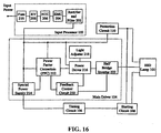
- FIG. 16 is a block diagram illustrating a circuit of a HID driver for a HID lamp according to another preferred embodiment of the invention.
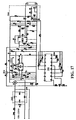
- FIG. 17 is a circuit diagram illustrating a circuit of a HID driver for a HID lamp according to a preferred embodiment of the invention.
- FIG. 16 and FIG. 17 may be a more detailed block diagram of a HID driver of FIG. 15 for illustrating the present invention.
- the input processor 102 further includes, for example but not limited to, one or more circuits selected from the group consisting of an rectifier and filter circuit 202, an electromagnetic wave controller (EMC) 204, a negative temperature control (NTC) resistor 206, a voltage sensitive resistor (RV) 208 and a fuse 210.
- the rectifier and filter circuit 202 includes, for example, a diode bridge circuit, a plurality of resistors, capacitors, and diodes and is provided for filtering and rectification.
- the electromagnetic wave controller (EMC) 204 is used for suppressing an electromagnetic wave interference including both radio-frequency and conductive-frequency interference.
- the main driver 104 includes, for example but not limited to, one or more circuits selected from the group consisting of a power factor. correction (PFC) circuit 212, a special power supply 214, a power driver 216, a light adjuster 218, a feedback control circuit 220, and a half bridge inverter 222.
- PFC power factor correction
- the power factor correction (PFC) circuit 212 is used for power factor correction and pre-regulation.
- the starting circuit 108 when the input power is low, the starting circuit 108 may not be necessary for the HID driver. Moreover, the timing circuit 106, for example, including the IC3 or the thyristor TH, may not be necessary for the HID driver.
- An AC input voltage of 85-305V, 50Hz/60Hz is inputted from the power input.
- the AC input voltage goes though the fuse, the negative temperature control (NTC) resistor and the voltage sensitive resistor (RV) for suppressing the transient over-voltage, the temporary over-voltage and the in-rush current of the AC input. Therefore, the AC input voltage is conditioned. Then the conditioned input voltage is inputted to the block 302 for electromagnetic wave control (EMC), wherein the block 302 may be used as an electromagnetic wave controller (EMC) 204.
- EMC electromagnetic wave control
- the circuit of the block 302 is constructed by a pair of capacitors C1 and C2 for suppressing the electromagnetic wave interference, and a pair of inductors, L1 and L1. Accordingly, the input processor 102 is used for conditioning and suppression the transients and in-rush current of the input power.
- the conditioned input voltage is 120V, 60Hz.
- a DC voltage with 120 Hz ripples supply to the primary and the control circuits.
- the voltage is applied to the power factor correction (PFC) circuit 212 to turn on the PFC circuit 212.
- the IC1 for example, an integrated circuit for power factor correlation is triggered by the DC voltage.
- a stable quasi-DC voltage in a range of about of 385-400V is outputted from the IC1 through the diode D4 and the capacitor C9.
- the quasi-DC voltage is supplied to the power driver 216 for power amplification.
- the quasi-DC voltage induced by the primary coil of inductor L2 of the PFC circuit 212, after being filtered and rectified, are applied to the IC2 and the IC3.
- the IC1 may be constructed by a conventional IC includes, for example but not limited to, L6561 or L6560 of ST, MC34261 or MC34262 of Motorola, TDA 4814 or TDA 4816 of Siemens, UC1852 or UC3852 of TI, SG3562 of Silicon General, KA7524 of Samsung.
- the IC2 includes, for example but not limited to, L6569 of ST.
- the IC3 includes, for example but not limited to, HCF4060BE of ST.
- all of the IC1 illustrated above have a limited dynamic range, particularly in a wide input voltage range.
- the power of the voltage can not exceed 150W.
- the ST developed the L4981A and the TI developed the UCC3817.
- the disadvantages of the two ICs are that the circuits and the required peripheral circuits of the two ICs are complex, the costs of the two ICs are high and the optimization of the circuits are also complex. Therefore, in the foregoing embodiment of the invention, a circuit using the traditional IC1 to achieved high power factor, low total harmonic distortion (THD), and high power output for wide input voltage range of IC2, the HID driver, is provided. It is noted that one of the functions of IC1 is closely related to preceding the filtering and rectification process.
- the inductor L2 is designed corresponding to the input voltage and power, the operating frequency, the magnitude of the ripple current, the suppressing effect to the electromagnetic wave, its location relative to the other circuit component, and the peripheral capacitor connected. Therefore, the basic property of the inductor L2 including, for example but not limited to, the material property and the type of the magnetic core, the number of the coils, the inductance, and the leakage of the magnetic core are all considered in the design of the electrical HID driver. For example, for a HID driver used for a low power loading, the inductor L2 is designed without an air gap.
- the inductor L2 is designed with an air gap and a higher capacitance of capacitor connected.
- the HID driver can provide a stable high power factor, low total harmonic distortion (THD) and low temperature increasing.
- the peripheral circuits of the PFC can be fine tuned by special design of the components.
- a resistance such as R11
- R11 can be divided into two resistors connected in parallel to reduce the uncertainty of the parameters.
- a key component of the power drive and amplification IC of the power driver is the inductance of the boost inductor.
- Vin(min) is the minimum input voltage
- D is the duty cycle
- Irip is the inductor ripple current
- F is the switching frequency. It is preferable that the duty cycle D is as large as possible.
- the ripple current is dependent on the stabilization of the working condition during the variation of the voltage, the current value and the activation ability.
- capacitor C9 Another important component is the capacitance of the power output capacitor, for example, capacitor C9.
- the capacitance C is, for example but not limited to, 150 ⁇ F/450V.
- the capacitance C is, for example but not limited to, 220 ⁇ F/450V or the capacitance C is a combination of using two capacitors of 470 ⁇ F/450V connected in serial.
- the capacitance C is 150 ⁇ F/450V.
- the 400W HPS HID driver can also work stably but with a higher temperature increment.
- a NTC is applied to the power input terminals of the HID driver for suppressing the in-rush current.
- the performance for suppressing the in-rush current of the NTC is not enough.
- a special design is provided for powering IC1, IC2, and IC3 suppressing the in-rush current during the starting period and hence prolonging the useful life of the HID lamp.
- IC1 receives input power through the resistor R3, filtering capacitor C4, and diode D3.
- PF power factor
- Vc high frequency voltage induced by the primary L2 that supplies IC1 through R7, D2, C5, and D1 and supplies IC2 and IC3 through R8 and R9 respectively. Therefore, in the very beginning during the starting period, R3 is not subject to a large current, and only, for example, a resistance of 2W or less of R3 is enough.
- the voltage applied to the IC2 of the secondary PWM power IC and the IC3 of the timing circuit is supplied by the voltage Vc induced by the primary L2. Therefore, the primary and the secondary coils of inductor L2 need to be fine-tuned according to each other.
- both the number of turns of the primary and the secondary coils of L2, as well as the ratio between the number of turns of the primary and the secondary coils are different from that of the conventional.
- the internal resistance of the cold lamp (before the lamp is turned on) is much larger than that of the lamp working in the normal condition.
- the current of the cold lamp is much smaller than the current of the lamp working in the normal condition.
- the resistor R12 connected to the leg 2 and the capacitor C11 connected to the leg 3 of IC2 is used to fine tune the main frequency of IC2.
- the parameter of the capacitor C12 can be fine tuned from 0.1 ⁇ F/50V to 1 ⁇ F/50V.
- the resistors R13, R14, R15 and R16 is used to improve the driving pulse of the output of IC2 at leg 5 and leg 7, thus, the power consumption during switching on and off can be reduced.
- the main frequency of the IC2 build-in voltage controlled oscillator (VCO) is set by the resistor R12 and capacitor C10.
- a larger output power can be obtained under a variety of voltages of working conditions.
- the first method includes, for example, replacing the half bridge power amplifier with a full bridge power amplifier.
- the second method includes modifying the design of the circuit 306 peripheral to the lamp.
- the circuit 306 can be replaced by the circuit 1902 shown in Figure 19. Referring to Figure 19, the terminal P1 of the lamp is still connected to the resistors R18, R19 and the capacitor C14, but the other terminal P2 is connected the capacitors Ca and Cb. Therefore, the total output power is decided by the capacitance of capacitors Ca and Cb.
- the output power of the HID driver can be enhanced to about 70W.
- the third method includes adjusting the capacitance of the capacitor C15.
- the capacitance is about 1 ⁇ F/400V.
- the output power is increased, and vice versa. It is important that the capacitance of the capacitor C 15 can not be too small, otherwise the low frequency components of the output voltage will be decreased and the opportunity of generating the sound resonance will be increased.
- a light adjuster 218 can be connected to the power driver 216, wherein the IC2 of the power driver 216 can also be used to adjust the brightness of the HID lamp by adjusting the frequency.
- the main frequency of IC2 is adjusted from the leg 2 and the leg 3 of IC2.
- the resistor R12 is connected in between the leg 2 and the leg 3 of IC2, and the capacitor C11 is connected to the leg 3 of IC2 to fine tune the main frequency of IC2.
- the resistance of the resistor R12 is preferably in a range of about 20K ⁇ to about 56K ⁇ . It is preferable that the light adjuster 218 is provided for a HID driver without an extremely large power output, and the length of the wire connected between the light adjuster 218 and the IC2 is as short as possible, otherwise the frequency will cause the sound resonance.
- the MOSFET M1, M2 and M3 source resistor detect the current passing through M1 and the power switch respectively and feedback simultaneously to adjust the operations of the PFC 212, the power switch circuit and the timing circuit 106.
- the present invention provides a novel and unique design of the starting circuit that can provide the HID driver with quick and reliable starting.
- a high voltage pulse must be provided to the HID lamp to discharge the gas.
- One starting circuit is provided by using the harmonic oscillation of the circuit, and the other is provided by using the bidirectional thyristor diodes (SIDAC). Accordingly, a starting circuit using the SIDAC is preferable since the amplitude and the width of the pulse obtained from the circuit is much easier to be controlled.
- SIDAC bidirectional thyristor diodes
- the starting circuit includes at least, for example but not limited to, a SIDAC connected in series to a diode D9 and the inductor L3.
- the diode D9 is not only used to ensure the single-direction of the current for charge and discharge, but also to prevent for the possibility of oscillation. Therefore, by adjusting the value and the period of the current simultaneously, the amplitude and the width of the high voltage pulse can be adjusted indirectly. When the capacitance of the charge capacitor C15 is also adjusted, the amplitude and the width of the high voltage pulse can be adjusted directly.
- a thyristor TH is connected to the capacitor C15, the SIDAC and the resistor R20. Therefore, when the control pole (gate) of the thyristor TH is at low voltage, both the thyristor TH and SIDAC are all in down condition, and the capacitor C15 is charged through the resistors R18 and R19. When the voltage across the capacitor C15 exceeds the collapse voltage V BO of SIDAC, the SIDAC is turn on while the thyristor is remained off; the capacitor C15 is subsequently discharged and a current through SIDAC, diode D9, inductor L3 is generated.
- the starting circuit is constructed by resistors R19, R18, capacitor C16, diode D9, SIDAC and inductor L3.
- the embodiment of the invention using the SIDAC as a starting circuit is preferably provided for the HPS lamp.
- the foregoing embodiment can also start the HML.
- the circuit 306 of FIG. 17 may be replaced by the circuit 2002 of FIG. 20. Referring to FIG. 20 the starting coil of inductor L3, the SIDAC, and D9 are eliminated and a capacitor is connected in parallel to the lamp.
- FIGS. 21 to 24 are circuit diagrams illustrating starting circuits of the HID driver according to embodiments of the invention.
- the circuit 306 of FIG. 17 can be replaced by any one of the circuits 2102, 2202, 2302, and 2402 of FIGS. 21, 22, 23 and 24 respectively.
- the circuits 2102, 2202, 2302, 2402 and the circuit 306 substantially have the same performance.
- the thyristor TH is off as its control pole is at low voltage.
- the current going through resistor R19 or resistors R18 and R19 will charge capacitor C15.
- the IC3 of the timing circuit 106 sends a pulse, for example, greater that 2V, to the gate of thyristor TH and turn on the thyristor TH.
- the capacitor C 15 then discharges to inductor L3 and start the lamp. Once the lamp is on, since thyristor TH is still on, the capacitor C15 can no longer be charged, and thus no more pulse will be generated.
- the present invention provides a novel and unique design of the protection circuit that is simple and effective.
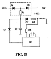
- IC1 and IC2 does not have any special protection function, however, the property of IC1, IC2, even though IC3 can be provided for the construction of the protection circuit.
- the power of IC1 is supplied through resistor R3 and capacitor C4.
- resistor R7, diode D2, capacitor C5 and diode D1 from the induced voltage of the primary coil of inductor L2.
- the power is supplied through resistors R8 and R9 to the PWM power driver IC2 and the timing circuit IC3 respectively.
- the resistors R7, R8, and R9 can be used to control the power supplies to IC1, IC2, and IC3. Therefore, in an embodiment of the invention, the design of the current protection circuit is based on the feature that, when the voltage of the power supplies to IC1, IC2, and IC3 drop to below a certain voltage, the IC1, IC2 and IC3 will get into a lockout condition.
- the output voltage of the HID driver when the lamp is in abnormal condition such as power failure, poor contact, broken lamp, etc, the output voltage of the HID driver will also drop. Consequently, the output voltage of the secondary and hence that of the primary coil will drop, causing IC2 and IC3 lockout. Since IC1 is still powered by current through resistor R3, capacitor C6, and diode D3, the IC1 gets into a condition that it can not be started. Therefore, the HID driver system is under the protection condition. The power consumption of the HID driver is thus reduced to a range of about 5W to about 10W, or even less than 5W that is only a fraction of 250W.
- the invention can also provide a preferable power consumption that supplies a sufficient large starting power and a low power in protection mode.
- the capacitor C6 can be adjusted to determine the power consumption.
- the mechanism that prevents the HID driver from stating after the HID lamp is turned on can also be provided as protection circuit.
- the timing circuit provides a starting pulse through resistor R21 to the control pole of the thyristor TH and thus the thyristor TH is turned on. Therefore, the charge remains on the capacitor C15 will be discharged and the charging and discharging process of the capacitor C15 including the generating of the high voltage pulses will be terminated until the next restarting period. Accordingly, the HID lamp can work normally and stably by the protection of the mechanism.
Landscapes
- Circuit Arrangements For Discharge Lamps (AREA)
- Rectifiers (AREA)
Applications Claiming Priority (2)
| Application Number | Priority Date | Filing Date | Title |
|---|---|---|---|
| US10/692,427 US7038396B2 (en) | 2003-10-22 | 2003-10-22 | Electronic high intensity discharge lamp driver |
| US692427 | 2003-10-22 |
Publications (2)
| Publication Number | Publication Date |
|---|---|
| EP1526763A1 true EP1526763A1 (de) | 2005-04-27 |
| EP1526763B1 EP1526763B1 (de) | 2007-04-25 |
Family
ID=34394571
Family Applications (1)
| Application Number | Title | Priority Date | Filing Date |
|---|---|---|---|
| EP04024298A Expired - Lifetime EP1526763B1 (de) | 2003-10-22 | 2004-10-12 | Steuerungsschaltung für eine elektronische Hochdruckentladungslampe |
Country Status (7)
| Country | Link |
|---|---|
| US (2) | US7038396B2 (de) |
| EP (1) | EP1526763B1 (de) |
| AT (1) | ATE360974T1 (de) |
| AU (2) | AU2004222714A1 (de) |
| CA (1) | CA2484690C (de) |
| DE (2) | DE04024298T1 (de) |
| ES (1) | ES2246750T1 (de) |
Cited By (1)
| Publication number | Priority date | Publication date | Assignee | Title |
|---|---|---|---|---|
| NL1032745C2 (nl) * | 2005-10-28 | 2009-04-22 | Luxtronic | Een energiesparende inrichting en werkwijze voor openbare verlichtingsinstallaties. |
Families Citing this family (17)
| Publication number | Priority date | Publication date | Assignee | Title |
|---|---|---|---|---|
| CN100508684C (zh) * | 2004-02-17 | 2009-07-01 | 楼方禄 | 大功率气体放电灯用电子控制器 |
| TWI285519B (en) * | 2005-11-04 | 2007-08-11 | Delta Electronics Inc | Method adopting square voltage waveform for driving flat lamps |
| CN2907170Y (zh) * | 2006-05-16 | 2007-05-30 | 彭俊忠 | 节电稳压镇流装置 |
| JP2007257944A (ja) * | 2006-03-22 | 2007-10-04 | Funai Electric Co Ltd | プロジェクタのランプ駆動装置 |
| CN201091080Y (zh) * | 2007-04-18 | 2008-07-23 | 富盟科技(深圳)有限公司 | 调光限电控制电路 |
| TWI455652B (zh) * | 2007-06-07 | 2014-10-01 | Delta Electronics Inc | 具相對較佳啟動與調光重啟動效果之介質阻擋放電燈系統及其驅動方法 |
| CN101336034B (zh) * | 2007-06-27 | 2012-08-22 | 台达电子工业股份有限公司 | 一种介质阻挡放电灯系统以及其驱动方法 |
| US20100188020A1 (en) * | 2009-01-26 | 2010-07-29 | Yeou Wang Enterprise Co., Ltd. | High frequency ballast for a fixed output high intensity discharge lamp |
| US20100270951A1 (en) * | 2009-04-27 | 2010-10-28 | Wen-Hsin Chao | Fluorescent lamp Having Overheat Protection Function |
| US8816593B2 (en) * | 2009-11-19 | 2014-08-26 | Koninklijke Philips N.V. | Method and apparatus selectively determining universal voltage input for solid state light fixtures |
| US10015860B2 (en) * | 2010-04-14 | 2018-07-03 | Philips Lighting Holding B.V. | Method and apparatus for detecting presence of dimmer and controlling power delivered to solid state lighting load |
| CO6530147A1 (es) * | 2011-09-23 | 2012-09-28 | Panacea Quantum Leap Technology Llc | Balaso electrónico |
| TWI484860B (zh) * | 2012-11-16 | 2015-05-11 | Beyond Innovation Tech Co Ltd | 關聯於發光二極體的負載驅動裝置 |
| CN106100128B (zh) * | 2016-07-27 | 2018-06-19 | 国网江苏省电力有限公司常州供电分公司 | 有源配电网智能终端蓄电池隔离监测装置 |
| EP3588757B1 (de) * | 2018-06-21 | 2020-08-19 | E+E Elektronik Ges.M.B.H. | Elektronische anordnung, optischer gassensor mit einer solchen elektronischen anordnung und verfahren zur leistungssteuerung einer strahlungsquelle mittels einer solchen elektronischen anordnung |
| TWI704754B (zh) * | 2019-12-11 | 2020-09-11 | 宏碁股份有限公司 | 電源供應器 |
| EP4011400B1 (de) * | 2020-12-11 | 2025-07-23 | The Boeing Company | System und verfahren zur desinfektion mit ultraviolettem licht mit verteilter energie |
Citations (5)
| Publication number | Priority date | Publication date | Assignee | Title |
|---|---|---|---|---|
| US5463287A (en) * | 1993-10-06 | 1995-10-31 | Tdk Corporation | Discharge lamp lighting apparatus which can control a lighting process |
| US5677602A (en) * | 1995-05-26 | 1997-10-14 | Paul; Jon D. | High efficiency electronic ballast for high intensity discharge lamps |
| US5942859A (en) * | 1997-04-18 | 1999-08-24 | Matsushita Electric Works, Ltd. | Discharge lamp lighting device |
| US6333607B1 (en) * | 1997-05-16 | 2001-12-25 | Denso Corporation | High voltage discharge lamp device |
| EP1322140A1 (de) * | 2000-09-26 | 2003-06-25 | Iwasaki Electric Co., Ltd | Schaltung für eine beleuchtungs-hid-lampe |
Family Cites Families (13)
| Publication number | Priority date | Publication date | Assignee | Title |
|---|---|---|---|---|
| US4672300A (en) * | 1985-03-29 | 1987-06-09 | Braydon Corporation | Direct current power supply using current amplitude modulation |
| US5030887A (en) * | 1990-01-29 | 1991-07-09 | Guisinger John E | High frequency fluorescent lamp exciter |
| US5428267A (en) * | 1992-07-09 | 1995-06-27 | Premier Power Systems, Inc. | Regulated DC power supply |
| KR950005283B1 (ko) * | 1992-10-08 | 1995-05-22 | 주식회사디엔에프전자 | 보호기능과 출력전압조절 및 조도조절이 가능한 초절전형 인버터회로 |
| US5321337A (en) * | 1992-11-12 | 1994-06-14 | Everay Electronic Co., Ltd. | Ballast having starting current restraint circuitry for preventing a large in-rush current and protection circuitry for preventing damage due to a start-up failure |
| US5327048A (en) * | 1993-02-26 | 1994-07-05 | North American Philips Corporation | Bi-level lighting control system for hid lamps |
| US5532894A (en) * | 1994-07-11 | 1996-07-02 | Minnesota Mining And Manufacturing Company | Overvoltage protection circuit |
| US6072282A (en) * | 1997-12-02 | 2000-06-06 | Power Circuit Innovations, Inc. | Frequency controlled quick and soft start gas discharge lamp ballast and method therefor |
| US6597127B2 (en) * | 2000-09-29 | 2003-07-22 | Matsushita Electric Industrial Co., Ltd. | Discharge lamp operating apparatus, self-ballasted discharge lamp, dimmer and illumination kit for dimming |
| WO2002093984A1 (en) * | 2001-05-16 | 2002-11-21 | Matsushita Electric Industrial Co., Ltd. | Discharge lamp lighting device and system comprising it |
| US6522089B1 (en) * | 2001-10-23 | 2003-02-18 | Orsam Sylvania Inc. | Electronic ballast and method for arc straightening |
| US6680585B2 (en) * | 2001-12-17 | 2004-01-20 | Osram Sylvania Inc. | Method and apparatus for modulating HID ballast operating frequency using DC bus ripple voltage |
| US6724152B2 (en) * | 2002-07-19 | 2004-04-20 | Donald K. Gladding | Lighting control system with variable arc control including start-up circuit for providing a bias voltage supply |
-
2003
- 2003-10-22 US US10/692,427 patent/US7038396B2/en not_active Expired - Lifetime
-
2004
- 2004-10-12 AT AT04024298T patent/ATE360974T1/de not_active IP Right Cessation
- 2004-10-12 DE DE04024298T patent/DE04024298T1/de active Pending
- 2004-10-12 DE DE602004006065T patent/DE602004006065D1/de not_active Expired - Lifetime
- 2004-10-12 EP EP04024298A patent/EP1526763B1/de not_active Expired - Lifetime
- 2004-10-12 ES ES04024298T patent/ES2246750T1/es active Pending
- 2004-10-14 CA CA002484690A patent/CA2484690C/en not_active Expired - Fee Related
- 2004-10-18 AU AU2004222714A patent/AU2004222714A1/en not_active Abandoned
-
2005
- 2005-08-05 US US11/197,883 patent/US7291988B2/en not_active Expired - Lifetime
-
2010
- 2010-05-24 AU AU2010202097A patent/AU2010202097A1/en not_active Abandoned
Patent Citations (5)
| Publication number | Priority date | Publication date | Assignee | Title |
|---|---|---|---|---|
| US5463287A (en) * | 1993-10-06 | 1995-10-31 | Tdk Corporation | Discharge lamp lighting apparatus which can control a lighting process |
| US5677602A (en) * | 1995-05-26 | 1997-10-14 | Paul; Jon D. | High efficiency electronic ballast for high intensity discharge lamps |
| US5942859A (en) * | 1997-04-18 | 1999-08-24 | Matsushita Electric Works, Ltd. | Discharge lamp lighting device |
| US6333607B1 (en) * | 1997-05-16 | 2001-12-25 | Denso Corporation | High voltage discharge lamp device |
| EP1322140A1 (de) * | 2000-09-26 | 2003-06-25 | Iwasaki Electric Co., Ltd | Schaltung für eine beleuchtungs-hid-lampe |
Cited By (1)
| Publication number | Priority date | Publication date | Assignee | Title |
|---|---|---|---|---|
| NL1032745C2 (nl) * | 2005-10-28 | 2009-04-22 | Luxtronic | Een energiesparende inrichting en werkwijze voor openbare verlichtingsinstallaties. |
Also Published As
| Publication number | Publication date |
|---|---|
| AU2004222714A1 (en) | 2005-05-12 |
| DE602004006065D1 (de) | 2007-06-06 |
| CA2484690A1 (en) | 2005-04-22 |
| US7291988B2 (en) | 2007-11-06 |
| ATE360974T1 (de) | 2007-05-15 |
| ES2246750T1 (es) | 2006-03-01 |
| EP1526763B1 (de) | 2007-04-25 |
| DE04024298T1 (de) | 2006-02-09 |
| CA2484690C (en) | 2007-03-20 |
| US20050088111A1 (en) | 2005-04-28 |
| AU2010202097A1 (en) | 2010-06-17 |
| US20060038503A1 (en) | 2006-02-23 |
| US7038396B2 (en) | 2006-05-02 |
Similar Documents
| Publication | Publication Date | Title |
|---|---|---|
| AU2010202097A1 (en) | Electronic high intensity discharge lamp driver | |
| US5932976A (en) | Discharge lamp driving | |
| US5677602A (en) | High efficiency electronic ballast for high intensity discharge lamps | |
| US6181076B1 (en) | Apparatus and method for operating a high intensity gas discharge lamp ballast | |
| KR20030051377A (ko) | 긴급 조명을 제공하는 전기 안정기 시스템 | |
| JPH0329298A (ja) | ガス放電ランプ用安定回路 | |
| CN102326454A (zh) | 用于气体放电灯的电子驱动装置 | |
| EP0922375B1 (de) | Universeller elektronischer starter für starkstromentladungslampen | |
| JP2002510844A (ja) | 高圧放電灯用電子式安定器 | |
| Ponce et al. | Analysis and design of igniters for HID lamps fed with square waveforms | |
| CA2533261A1 (en) | Circuit for operating high-pressure discharge lamps | |
| CN201114945Y (zh) | 高压放电灯电子镇流器 | |
| JP5014418B2 (ja) | 蛍光ランプ用電子ドライバ | |
| Corominas et al. | A novel low cost two-stage electronic ballast for 250 W high pressure mercury vapor lamps based on current-mode-controlled buck-boost inverter | |
| JP2003203790A (ja) | 放電灯点灯装置 | |
| KR100431077B1 (ko) | 고압방전 램프용 구동회로 | |
| CN103313494A (zh) | 低频半桥hid安定器、高压气体放电灯及驱动方法 | |
| CN101351070A (zh) | 高强度放电灯镇流器电路 | |
| KR200253226Y1 (ko) | 고압방전 램프용 구동회로 | |
| Divakar et al. | Examination of the power conditioning driving circuit for automotive HID lamp | |
| JPH08339891A (ja) | 放電灯点灯装置 | |
| KR20090119579A (ko) | 방전등용 전자식 안정기 회로 | |
| JP2003203794A (ja) | 高圧放電灯用の高周波電子式安定器 | |
| KR20030004636A (ko) | 전자식 안정기 | |
| KR20030000026A (ko) | 방전등의 점등회로 |
Legal Events
| Date | Code | Title | Description |
|---|---|---|---|
| PUAI | Public reference made under article 153(3) epc to a published international application that has entered the european phase |
Free format text: ORIGINAL CODE: 0009012 |
|
| AK | Designated contracting states |
Kind code of ref document: A1 Designated state(s): AT BE BG CH CY CZ DE DK EE ES FI FR GB GR HU IE IT LI LU MC NL PL PT RO SE SI SK TR |
|
| AX | Request for extension of the european patent |
Extension state: AL HR LT LV MK |
|
| REG | Reference to a national code |
Ref country code: SE Ref legal event code: TRCL |
|
| EL | Fr: translation of claims filed | ||
| 17P | Request for examination filed |
Effective date: 20051007 |
|
| TCNL | Nl: translation of patent claims filed | ||
| AKX | Designation fees paid |
Designated state(s): AT BE BG CH CY CZ DE DK EE ES FI FR GB GR HU IE IT LI LU MC NL PL PT RO SE SI SK TR |
|
| DET | De: translation of patent claims | ||
| GRAP | Despatch of communication of intention to grant a patent |
Free format text: ORIGINAL CODE: EPIDOSNIGR1 |
|
| GRAS | Grant fee paid |
Free format text: ORIGINAL CODE: EPIDOSNIGR3 |
|
| GRAA | (expected) grant |
Free format text: ORIGINAL CODE: 0009210 |
|
| AK | Designated contracting states |
Kind code of ref document: B1 Designated state(s): AT BE BG CH CY CZ DE DK EE ES FI FR GB GR HU IE IT LI LU MC NL PL PT RO SE SI SK TR |
|
| PG25 | Lapsed in a contracting state [announced via postgrant information from national office to epo] |
Ref country code: CH Free format text: LAPSE BECAUSE OF FAILURE TO SUBMIT A TRANSLATION OF THE DESCRIPTION OR TO PAY THE FEE WITHIN THE PRESCRIBED TIME-LIMIT Effective date: 20070425 Ref country code: LI Free format text: LAPSE BECAUSE OF FAILURE TO SUBMIT A TRANSLATION OF THE DESCRIPTION OR TO PAY THE FEE WITHIN THE PRESCRIBED TIME-LIMIT Effective date: 20070425 Ref country code: FI Free format text: LAPSE BECAUSE OF FAILURE TO SUBMIT A TRANSLATION OF THE DESCRIPTION OR TO PAY THE FEE WITHIN THE PRESCRIBED TIME-LIMIT Effective date: 20070425 |
|
| REG | Reference to a national code |
Ref country code: GB Ref legal event code: FG4D |
|
| REG | Reference to a national code |
Ref country code: IE Ref legal event code: FG4D |
|
| REG | Reference to a national code |
Ref country code: CH Ref legal event code: EP |
|
| REF | Corresponds to: |
Ref document number: 602004006065 Country of ref document: DE Date of ref document: 20070606 Kind code of ref document: P |
|
| PG25 | Lapsed in a contracting state [announced via postgrant information from national office to epo] |
Ref country code: SE Free format text: LAPSE BECAUSE OF FAILURE TO SUBMIT A TRANSLATION OF THE DESCRIPTION OR TO PAY THE FEE WITHIN THE PRESCRIBED TIME-LIMIT Effective date: 20070725 |
|
| PG25 | Lapsed in a contracting state [announced via postgrant information from national office to epo] |
Ref country code: ES Free format text: LAPSE BECAUSE OF FAILURE TO SUBMIT A TRANSLATION OF THE DESCRIPTION OR TO PAY THE FEE WITHIN THE PRESCRIBED TIME-LIMIT Effective date: 20070805 |
|
| PG25 | Lapsed in a contracting state [announced via postgrant information from national office to epo] |
Ref country code: PT Free format text: LAPSE BECAUSE OF FAILURE TO SUBMIT A TRANSLATION OF THE DESCRIPTION OR TO PAY THE FEE WITHIN THE PRESCRIBED TIME-LIMIT Effective date: 20070925 |
|
| REG | Reference to a national code |
Ref country code: CH Ref legal event code: PL |
|
| NLV1 | Nl: lapsed or annulled due to failure to fulfill the requirements of art. 29p and 29m of the patents act | ||
| PG25 | Lapsed in a contracting state [announced via postgrant information from national office to epo] |
Ref country code: PL Free format text: LAPSE BECAUSE OF FAILURE TO SUBMIT A TRANSLATION OF THE DESCRIPTION OR TO PAY THE FEE WITHIN THE PRESCRIBED TIME-LIMIT Effective date: 20070425 Ref country code: AT Free format text: LAPSE BECAUSE OF FAILURE TO SUBMIT A TRANSLATION OF THE DESCRIPTION OR TO PAY THE FEE WITHIN THE PRESCRIBED TIME-LIMIT Effective date: 20070425 |
|
| EN | Fr: translation not filed | ||
| PG25 | Lapsed in a contracting state [announced via postgrant information from national office to epo] |
Ref country code: BE Free format text: LAPSE BECAUSE OF FAILURE TO SUBMIT A TRANSLATION OF THE DESCRIPTION OR TO PAY THE FEE WITHIN THE PRESCRIBED TIME-LIMIT Effective date: 20070425 |
|
| PG25 | Lapsed in a contracting state [announced via postgrant information from national office to epo] |
Ref country code: DK Free format text: LAPSE BECAUSE OF FAILURE TO SUBMIT A TRANSLATION OF THE DESCRIPTION OR TO PAY THE FEE WITHIN THE PRESCRIBED TIME-LIMIT Effective date: 20070425 Ref country code: BG Free format text: LAPSE BECAUSE OF FAILURE TO SUBMIT A TRANSLATION OF THE DESCRIPTION OR TO PAY THE FEE WITHIN THE PRESCRIBED TIME-LIMIT Effective date: 20070725 Ref country code: CZ Free format text: LAPSE BECAUSE OF FAILURE TO SUBMIT A TRANSLATION OF THE DESCRIPTION OR TO PAY THE FEE WITHIN THE PRESCRIBED TIME-LIMIT Effective date: 20070425 Ref country code: NL Free format text: LAPSE BECAUSE OF FAILURE TO SUBMIT A TRANSLATION OF THE DESCRIPTION OR TO PAY THE FEE WITHIN THE PRESCRIBED TIME-LIMIT Effective date: 20070425 Ref country code: SI Free format text: LAPSE BECAUSE OF FAILURE TO SUBMIT A TRANSLATION OF THE DESCRIPTION OR TO PAY THE FEE WITHIN THE PRESCRIBED TIME-LIMIT Effective date: 20070425 |
|
| PG25 | Lapsed in a contracting state [announced via postgrant information from national office to epo] |
Ref country code: SK Free format text: LAPSE BECAUSE OF FAILURE TO SUBMIT A TRANSLATION OF THE DESCRIPTION OR TO PAY THE FEE WITHIN THE PRESCRIBED TIME-LIMIT Effective date: 20070425 |
|
| PLBE | No opposition filed within time limit |
Free format text: ORIGINAL CODE: 0009261 |
|
| STAA | Information on the status of an ep patent application or granted ep patent |
Free format text: STATUS: NO OPPOSITION FILED WITHIN TIME LIMIT |
|
| 26N | No opposition filed |
Effective date: 20080128 |
|
| PG25 | Lapsed in a contracting state [announced via postgrant information from national office to epo] |
Ref country code: DE Free format text: LAPSE BECAUSE OF FAILURE TO SUBMIT A TRANSLATION OF THE DESCRIPTION OR TO PAY THE FEE WITHIN THE PRESCRIBED TIME-LIMIT Effective date: 20070726 Ref country code: GR Free format text: LAPSE BECAUSE OF FAILURE TO SUBMIT A TRANSLATION OF THE DESCRIPTION OR TO PAY THE FEE WITHIN THE PRESCRIBED TIME-LIMIT Effective date: 20070726 Ref country code: FR Free format text: LAPSE BECAUSE OF FAILURE TO SUBMIT A TRANSLATION OF THE DESCRIPTION OR TO PAY THE FEE WITHIN THE PRESCRIBED TIME-LIMIT Effective date: 20071221 Ref country code: IT Free format text: LAPSE BECAUSE OF FAILURE TO SUBMIT A TRANSLATION OF THE DESCRIPTION OR TO PAY THE FEE WITHIN THE PRESCRIBED TIME-LIMIT Effective date: 20070425 |
|
| PG25 | Lapsed in a contracting state [announced via postgrant information from national office to epo] |
Ref country code: MC Free format text: LAPSE BECAUSE OF NON-PAYMENT OF DUE FEES Effective date: 20071031 Ref country code: RO Free format text: LAPSE BECAUSE OF FAILURE TO SUBMIT A TRANSLATION OF THE DESCRIPTION OR TO PAY THE FEE WITHIN THE PRESCRIBED TIME-LIMIT Effective date: 20070425 |
|
| PG25 | Lapsed in a contracting state [announced via postgrant information from national office to epo] |
Ref country code: IE Free format text: LAPSE BECAUSE OF NON-PAYMENT OF DUE FEES Effective date: 20071012 |
|
| PG25 | Lapsed in a contracting state [announced via postgrant information from national office to epo] |
Ref country code: FR Free format text: LAPSE BECAUSE OF FAILURE TO SUBMIT A TRANSLATION OF THE DESCRIPTION OR TO PAY THE FEE WITHIN THE PRESCRIBED TIME-LIMIT Effective date: 20070425 |
|
| PG25 | Lapsed in a contracting state [announced via postgrant information from national office to epo] |
Ref country code: EE Free format text: LAPSE BECAUSE OF FAILURE TO SUBMIT A TRANSLATION OF THE DESCRIPTION OR TO PAY THE FEE WITHIN THE PRESCRIBED TIME-LIMIT Effective date: 20070425 |
|
| GBPC | Gb: european patent ceased through non-payment of renewal fee |
Effective date: 20081012 |
|
| PG25 | Lapsed in a contracting state [announced via postgrant information from national office to epo] |
Ref country code: CY Free format text: LAPSE BECAUSE OF FAILURE TO SUBMIT A TRANSLATION OF THE DESCRIPTION OR TO PAY THE FEE WITHIN THE PRESCRIBED TIME-LIMIT Effective date: 20070425 |
|
| PG25 | Lapsed in a contracting state [announced via postgrant information from national office to epo] |
Ref country code: LU Free format text: LAPSE BECAUSE OF NON-PAYMENT OF DUE FEES Effective date: 20071012 |
|
| PG25 | Lapsed in a contracting state [announced via postgrant information from national office to epo] |
Ref country code: TR Free format text: LAPSE BECAUSE OF FAILURE TO SUBMIT A TRANSLATION OF THE DESCRIPTION OR TO PAY THE FEE WITHIN THE PRESCRIBED TIME-LIMIT Effective date: 20070425 Ref country code: HU Free format text: LAPSE BECAUSE OF FAILURE TO SUBMIT A TRANSLATION OF THE DESCRIPTION OR TO PAY THE FEE WITHIN THE PRESCRIBED TIME-LIMIT Effective date: 20071026 |
|
| PG25 | Lapsed in a contracting state [announced via postgrant information from national office to epo] |
Ref country code: GB Free format text: LAPSE BECAUSE OF NON-PAYMENT OF DUE FEES Effective date: 20081012 |