EP1526110A2 - Chip en semiconducteur de type n aven un nanopore. - Google Patents
Chip en semiconducteur de type n aven un nanopore. Download PDFInfo
- Publication number
- EP1526110A2 EP1526110A2 EP04015777A EP04015777A EP1526110A2 EP 1526110 A2 EP1526110 A2 EP 1526110A2 EP 04015777 A EP04015777 A EP 04015777A EP 04015777 A EP04015777 A EP 04015777A EP 1526110 A2 EP1526110 A2 EP 1526110A2
- Authority
- EP
- European Patent Office
- Prior art keywords
- nanopore
- type semiconductor
- semiconductor
- chip
- ionic solution
- Prior art date
- Legal status (The legal status is an assumption and is not a legal conclusion. Google has not performed a legal analysis and makes no representation as to the accuracy of the status listed.)
- Withdrawn
Links
- 239000004065 semiconductor Substances 0.000 title claims abstract description 41
- 238000000034 method Methods 0.000 claims abstract description 19
- 238000004519 manufacturing process Methods 0.000 claims abstract description 9
- 229910052710 silicon Inorganic materials 0.000 claims description 14
- 239000010703 silicon Substances 0.000 claims description 14
- 229910052785 arsenic Inorganic materials 0.000 claims description 6
- RQNWIZPPADIBDY-UHFFFAOYSA-N arsenic atom Chemical compound [As] RQNWIZPPADIBDY-UHFFFAOYSA-N 0.000 claims description 6
- 239000002019 doping agent Substances 0.000 claims description 6
- BHEPBYXIRTUNPN-UHFFFAOYSA-N hydridophosphorus(.) (triplet) Chemical compound [PH] BHEPBYXIRTUNPN-UHFFFAOYSA-N 0.000 claims description 6
- JBRZTFJDHDCESZ-UHFFFAOYSA-N AsGa Chemical compound [As]#[Ga] JBRZTFJDHDCESZ-UHFFFAOYSA-N 0.000 claims description 3
- 229910001218 Gallium arsenide Inorganic materials 0.000 claims description 3
- 229910052732 germanium Inorganic materials 0.000 claims description 3
- GNPVGFCGXDBREM-UHFFFAOYSA-N germanium atom Chemical compound [Ge] GNPVGFCGXDBREM-UHFFFAOYSA-N 0.000 claims description 3
- 206010034972 Photosensitivity reaction Diseases 0.000 abstract description 11
- 230000036211 photosensitivity Effects 0.000 abstract description 11
- 230000001747 exhibiting effect Effects 0.000 abstract description 2
- XUIMIQQOPSSXEZ-UHFFFAOYSA-N Silicon Chemical compound [Si] XUIMIQQOPSSXEZ-UHFFFAOYSA-N 0.000 description 10
- 239000000463 material Substances 0.000 description 10
- 108020004414 DNA Proteins 0.000 description 6
- 238000010884 ion-beam technique Methods 0.000 description 6
- WCUXLLCKKVVCTQ-UHFFFAOYSA-M Potassium chloride Chemical compound [Cl-].[K+] WCUXLLCKKVVCTQ-UHFFFAOYSA-M 0.000 description 5
- 238000006073 displacement reaction Methods 0.000 description 5
- 239000012212 insulator Substances 0.000 description 5
- 230000000593 degrading effect Effects 0.000 description 4
- 239000012528 membrane Substances 0.000 description 4
- 239000002105 nanoparticle Substances 0.000 description 4
- 238000004806 packaging method and process Methods 0.000 description 4
- 239000000758 substrate Substances 0.000 description 4
- 238000013459 approach Methods 0.000 description 3
- XKRFYHLGVUSROY-UHFFFAOYSA-N Argon Chemical compound [Ar] XKRFYHLGVUSROY-UHFFFAOYSA-N 0.000 description 2
- VYPSYNLAJGMNEJ-UHFFFAOYSA-N Silicium dioxide Chemical compound O=[Si]=O VYPSYNLAJGMNEJ-UHFFFAOYSA-N 0.000 description 2
- 239000000460 chlorine Substances 0.000 description 2
- 229910052801 chlorine Inorganic materials 0.000 description 2
- -1 chlorine ions Chemical class 0.000 description 2
- 238000013461 design Methods 0.000 description 2
- 230000007774 longterm Effects 0.000 description 2
- 230000000873 masking effect Effects 0.000 description 2
- 238000005259 measurement Methods 0.000 description 2
- 239000011148 porous material Substances 0.000 description 2
- 239000001103 potassium chloride Substances 0.000 description 2
- 235000011164 potassium chloride Nutrition 0.000 description 2
- 229910001414 potassium ion Inorganic materials 0.000 description 2
- 238000001228 spectrum Methods 0.000 description 2
- 230000001052 transient effect Effects 0.000 description 2
- 102000053602 DNA Human genes 0.000 description 1
- 229910052581 Si3N4 Inorganic materials 0.000 description 1
- 238000009825 accumulation Methods 0.000 description 1
- 229910052786 argon Inorganic materials 0.000 description 1
- 238000004891 communication Methods 0.000 description 1
- 238000010276 construction Methods 0.000 description 1
- 230000008878 coupling Effects 0.000 description 1
- 238000010168 coupling process Methods 0.000 description 1
- 238000005859 coupling reaction Methods 0.000 description 1
- 238000005553 drilling Methods 0.000 description 1
- 238000005530 etching Methods 0.000 description 1
- 230000008020 evaporation Effects 0.000 description 1
- 238000001704 evaporation Methods 0.000 description 1
- 239000010416 ion conductor Substances 0.000 description 1
- 239000007788 liquid Substances 0.000 description 1
- 229910052751 metal Inorganic materials 0.000 description 1
- 239000002184 metal Substances 0.000 description 1
- 239000000203 mixture Substances 0.000 description 1
- 238000012986 modification Methods 0.000 description 1
- 230000004048 modification Effects 0.000 description 1
- 108020004707 nucleic acids Proteins 0.000 description 1
- 102000039446 nucleic acids Human genes 0.000 description 1
- 150000007523 nucleic acids Chemical class 0.000 description 1
- 108091033319 polynucleotide Proteins 0.000 description 1
- 102000040430 polynucleotide Human genes 0.000 description 1
- 239000002157 polynucleotide Substances 0.000 description 1
- 238000011160 research Methods 0.000 description 1
- 238000012163 sequencing technique Methods 0.000 description 1
- 239000000377 silicon dioxide Substances 0.000 description 1
- 235000012239 silicon dioxide Nutrition 0.000 description 1
- HQVNEWCFYHHQES-UHFFFAOYSA-N silicon nitride Chemical compound N12[Si]34N5[Si]62N3[Si]51N64 HQVNEWCFYHHQES-UHFFFAOYSA-N 0.000 description 1
- 239000007787 solid Substances 0.000 description 1
- 239000000126 substance Substances 0.000 description 1
- 238000012795 verification Methods 0.000 description 1
Images
Classifications
-
- B—PERFORMING OPERATIONS; TRANSPORTING
- B81—MICROSTRUCTURAL TECHNOLOGY
- B81C—PROCESSES OR APPARATUS SPECIALLY ADAPTED FOR THE MANUFACTURE OR TREATMENT OF MICROSTRUCTURAL DEVICES OR SYSTEMS
- B81C1/00—Manufacture or treatment of devices or systems in or on a substrate
- B81C1/00015—Manufacture or treatment of devices or systems in or on a substrate for manufacturing microsystems
- B81C1/00023—Manufacture or treatment of devices or systems in or on a substrate for manufacturing microsystems without movable or flexible elements
- B81C1/00087—Holes
-
- G—PHYSICS
- G01—MEASURING; TESTING
- G01N—INVESTIGATING OR ANALYSING MATERIALS BY DETERMINING THEIR CHEMICAL OR PHYSICAL PROPERTIES
- G01N33/00—Investigating or analysing materials by specific methods not covered by groups G01N1/00 - G01N31/00
- G01N33/48—Biological material, e.g. blood, urine; Haemocytometers
- G01N33/483—Physical analysis of biological material
- G01N33/487—Physical analysis of biological material of liquid biological material
- G01N33/48707—Physical analysis of biological material of liquid biological material by electrical means
- G01N33/48721—Investigating individual macromolecules, e.g. by translocation through nanopores
-
- B—PERFORMING OPERATIONS; TRANSPORTING
- B81—MICROSTRUCTURAL TECHNOLOGY
- B81B—MICROSTRUCTURAL DEVICES OR SYSTEMS, e.g. MICROMECHANICAL DEVICES
- B81B2201/00—Specific applications of microelectromechanical systems
- B81B2201/05—Microfluidics
- B81B2201/058—Microfluidics not provided for in B81B2201/051 - B81B2201/054
-
- B—PERFORMING OPERATIONS; TRANSPORTING
- B81—MICROSTRUCTURAL TECHNOLOGY
- B81B—MICROSTRUCTURAL DEVICES OR SYSTEMS, e.g. MICROMECHANICAL DEVICES
- B81B2203/00—Basic microelectromechanical structures
- B81B2203/01—Suspended structures, i.e. structures allowing a movement
- B81B2203/0127—Diaphragms, i.e. structures separating two media that can control the passage from one medium to another; Membranes, i.e. diaphragms with filtering function
Definitions
- the invention relates generally to the field of nanopores and more particularly to an apparatus and method for making a nanopore chip exhibiting one of low photosensitivity, low electrical noise, and low electrical drift.
- Manipulating matter at the nanometer scale is important for many electronic, chemical and biological advances (See Li et al ., "Ion beam sculpting at nanometer length scales", Nature, 412 : 166-169, 2001). Such techniques as “ion beam sculpting” have shown promise in fabricating molecule scale holes and nanopores in thin insulating membranes. These pores have also been effective in localizing molecular-scale electrical junctions and switches (See Li et al ., “Ion beam sculpting at nanometer length scales", Nature, 412 : 166-169, 2001).
- Nanopores have been fabricated by a variety of research groups with a number of materials. Generally, the approach is to fabricate these nanopores in a solidstate material or a thin freestanding diaphragm of material supported on a frame of thick silicon to form a nanopore chip.
- Some materials that have been used to date for the diaphragm material include silicon nitride and silicon dioxide. These materials are insulators, with resistivity typically greater than 10 10 Ohm-cm. In contrast, silicon is a semiconductor with a resistivity less than 10 4 Ohm-cm, and for practical purposes can be considered to be a near short circuit in relation to the insulating diaphragm material.
- Data is typically obtained from an artificial nanopore by placing the nanopore in an aqueous ionic solution of potassium chloride (KCl), commonly referred to as a "buffer” solution, the solution containing molecules of a polynucleotide such as doublestranded DNA.
- KCl potassium chloride
- Buffer buffer solution
- Figure 1b from that reference is reproduced herein as FIG. 1.
- a voltage V is applied across the nanopore by electrodes located in the "Cis” and “Trans” volumes, and the resulting current is measured as an "Ionic current signal.”
- the invention provides an apparatus and method for nanopore construction.
- the apparatus comprises a nanopore chip comprising a nanopore disposed in an insulating diaphragm, the diaphragm being supported by a rigid frame, the rigid frame comprising an N-type semiconductor in those portions of the nanopore chip which are intended to be capacitively coupled to an ionic solution.
- the invention also provides a method of making the apparatus.
- the method of making the apparatus comprises fabricating a nanopore chip by
- the steps of the above method may be varied in any logically consistent fashion.
- the nanopore may be formed before or after the diaphragm is formed.
- the providing of N-type doping may occur before or after the diaphragm is formed.
- Methods recited herein may be carried out in any order of the recited events that is logically possible, as well as the recited order of events.
- Nanopore refers to any pore or hole between at least a pair of electrodes or a hole in a solid substrate. Nanopores can range in size and can range from about 1 nm to about 300 nm. Most effective nanopores have been roughly around 2 nm.
- adjacent refers to anything that is near, next to or adjoining.
- a tensile layer may be near a compressive layer, next to a compressive layer or adjoining a compressive layer.
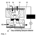
- FIG. 1 shows a cross section the apparatus of the present invention packaged for use with associated ionic solutions and electronics.
- the figure is not to scale, and some features are greatly exaggerated for purposes of description.
- the nanopore is very small in comparison to the width of the diaphragm and is not explicitly shown in the drawing, but that nanopore sits in the thin diaphragm atop the "Chip containing nanopore detector,” herein called a "nanopore chip.”
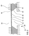
- FIG. 2 shows a corss ection of the apparatus of the present invention with some associated packaging elements.
- a voltage V typically on the order of 120 millivolts, is applied between the "Cis”volume 24 and “Trans” volume 26 of aqueous ionic KCl solution.
- DNA molecules which have a negative charge and are labeled "DNA - " to denote that charge, sit in the CIS volume 24 and are drawn by the voltage difference between the Cis and Trans volumes 24 and 26 to the nanopore 12 in the thin insulating diaphragm 14 atop the nanopore chip 10, through that nanopore 12, and into the Trans volume 26.
- an ionic stream, not shown, comprising negatively charged hydrated chlorine ions flow from Cis to Trans
- an ionic stream, not shown, comprising positively charged hydrated potassium ions flows from Trans to Cis.
- Packaging element 20 confines the ionic solution to the Cis volume 24 while packaging element 22 confines the ionic solution to the Trans volume 26.
- the total measured "ionic current signal” comprises not only charge flows due to the DNA, the chlorine ions, and the potassium ions, but also comprises undesired displacement currents having transient characteristics (called “AC characteristics”) with some magnitude and some frequency spectrum, but having zero net long-term characteristics (called “DC characteristics”). These displacement currents occur across the insulating diaphragm 14 in which the nanopore 12 sits, across the capacitively-coupled interfaces 28 between the semiconductor frame 18 and the Trans volume 26, and across the capacitively coupled interface 30 between the semiconductor frame 18 and the Cis volume 24
- the current through the nanopore 12 has both a DC characteristic and an AC characteristic, the AC characteristic having some frequency spectrum.
- the desired signal is degraded to some extent.
- one approach is to minimize capacitance either through packaging design, through modification to the nanopore chip for example as in patent application (Docket 10021090-1, APPARATUS AND METHOD FOR MAKING A LOW CAPACITANCE ARTIFICIAL NANOPORE, which is incorporated herein in its entirety by reference), or both.
- the inventor has proposed the use of n-type silicon instead of p-type silicon to fabricate the semiconductor frame 18 of nanopore chips in the belief that such chips would have an accumulation region, rather than a depletion region, near region 28 and region 30, and that such chips would exhibit greatly reduced photosensitivity of the ionic current. Such chips have been fabricated, and the expected reduction in photosensitivity has been achieved. As of this writing, no measurements of transients and long-term drift have been conducted. The present invention is expected to show utility in reducing transients, electrical noise, and electrical drift.
- n-type silicon doped with phosphorous having a resistivity in the range of 1-50 Ohm-cm.
- Other n-type semiconductors may be used, including but not limited to germanium and gallium arsenide, and for such other n-type semiconductors known n-type dopants may be used, including but not limited to phosphorous and arsenic.
- microscale dimensions are defined to include dimensions from 100 nm to 1 mm
- nanoscale dimensions are defined to include dimension from 0.1 nm to 1 um.
- the present invention comprises a chip apparatus for use in a package comprising an ionic solution, the chip apparatus having an insulating diaphragm, one of a microscale and a nanoscale device disposed one of in or on the insulating diaphragm, and a semiconductor frame supporting the insulating diaphragm, wherein those portions of the semiconductor frame which are to be capacitively coupled to an ionic solution, the ionic solution also to be electrically coupled to the one of a microscale and a nanoscale device, comprise an n-type semiconductor, comprising typically n-type silicon.
- FIG. 1 shows the cavity on the bottom side of the diaphragm extending entirely through the thickness of the semiconductor frame, this is not a necessity of the invention, and instead the cavity beneath the diaphragm may occupy a limited portion of the thickness of the semiconductor frame.
- a limited area of p-type semiconductor may intrude into the portions of the semiconductor frame 18 which are to be capacitively coupled to an ionic solution without significantly degrading the performance of the present invention. Such regions are expected to increase photosensitivity, noise, and drift, but such increases will be tolerated as part of desirable performance tradeoffs when, for example, active electronic elements are integrated into the nanopore chip.
- a limited area of semiconductor may intrude into the insulating diaphragm 14 without significantly degrading the performance of the present invention. Such regions are expected to increase photosensitivity, noise, and drift, but such increases will be tolerated as part of desirable performance tradeoffs when, for example, active electronic elements are integrated into the nanopore chip.
- a limited area of metal may intrude into the insulating diaphragm 14 without significantly degrading the performance of the present invention. Such regions are expected to increase photosensitivity, noise, and drift, but such increases will be tolerated as part of desirable performance tradeoffs when, for example, active electronic elements are integrated into the nanopore chip.
- the present invention also comprises a method of fabricating a chip apparatus for use in a package comprising an ionic solution, comprising providing a semiconductor frame, providing n-type semiconductor regions comprising those portions of the semiconductor frame which are to be capacitively coupled to an ionic solution, providing an insulating diaphragm supported by the semiconductor frame, and providing one of a microscale and a nanoscale device disposed one of in or on the insulating diaphragm, the ionic solution also to be electrically coupled to the one of a microscale and a nanoscale device.
- a nanopore may be accomplished by means other than focused ion beam drilling and argon ion beam sculpting described in Li et al ., "Ion beam sculpting at nanometer length scales", Nature, 412 : 166-169, 2001.
- other known means of fabricating a nanopore include masking with a nanoparticle followed by layer evaporation around the masking nanoparticle, next followed by removal of the nanoparticle and etching within the hole which had been masked by the nanoparticle.
- Such techniques both known and unknown, may be used to fabricate nanopores as part of the apparatus and method of the present invention.
Landscapes
- Engineering & Computer Science (AREA)
- Health & Medical Sciences (AREA)
- Chemical & Material Sciences (AREA)
- Life Sciences & Earth Sciences (AREA)
- Physics & Mathematics (AREA)
- Biomedical Technology (AREA)
- Manufacturing & Machinery (AREA)
- Analytical Chemistry (AREA)
- Food Science & Technology (AREA)
- Biochemistry (AREA)
- Molecular Biology (AREA)
- Urology & Nephrology (AREA)
- Biophysics (AREA)
- Medicinal Chemistry (AREA)
- Spectroscopy & Molecular Physics (AREA)
- Hematology (AREA)
- General Health & Medical Sciences (AREA)
- General Physics & Mathematics (AREA)
- Immunology (AREA)
- Pathology (AREA)
- Nanotechnology (AREA)
- Microelectronics & Electronic Packaging (AREA)
- Investigating Or Analyzing Materials By The Use Of Electric Means (AREA)
- Light Receiving Elements (AREA)
Applications Claiming Priority (2)
| Application Number | Priority Date | Filing Date | Title |
|---|---|---|---|
| US10/693,060 US6846702B1 (en) | 2003-10-24 | 2003-10-24 | Nanopore chip with N-type semiconductor |
| US693060P | 2003-10-24 |
Publications (2)
| Publication Number | Publication Date |
|---|---|
| EP1526110A2 true EP1526110A2 (fr) | 2005-04-27 |
| EP1526110A3 EP1526110A3 (fr) | 2005-10-12 |
Family
ID=34063557
Family Applications (1)
| Application Number | Title | Priority Date | Filing Date |
|---|---|---|---|
| EP04015777A Withdrawn EP1526110A3 (fr) | 2003-10-24 | 2004-07-05 | Chip en semiconducteur de type n aven un nanopore. |
Country Status (2)
| Country | Link |
|---|---|
| US (2) | US6846702B1 (fr) |
| EP (1) | EP1526110A3 (fr) |
Families Citing this family (17)
| Publication number | Priority date | Publication date | Assignee | Title |
|---|---|---|---|---|
| WO2001016047A2 (fr) * | 1999-08-18 | 2001-03-08 | Rutgers, The State University | Ceramique composite a taille de grain nanometrique et son procede de fabrication |
| US7075161B2 (en) * | 2003-10-23 | 2006-07-11 | Agilent Technologies, Inc. | Apparatus and method for making a low capacitance artificial nanopore |
| US6846702B1 (en) * | 2003-10-24 | 2005-01-25 | Agilent Technologies, Inc. | Nanopore chip with N-type semiconductor |
| JP4897681B2 (ja) * | 2004-07-23 | 2012-03-14 | エレクトロニック・バイオサイエンシーズ・エルエルシー | イオン・チャネルを通過する時間的に変化する電流を検出するための方法及び装置 |
| US7114378B1 (en) | 2005-04-14 | 2006-10-03 | Agilent Technologies, Inc. | Planar resonant tunneling sensor and method of fabricating and using the same |
| US20060231419A1 (en) * | 2005-04-15 | 2006-10-19 | Barth Philip W | Molecular resonant tunneling sensor and methods of fabricating and using the same |
| IT1393996B1 (it) * | 2008-09-18 | 2012-05-17 | Univ Degli Studi Genova | Dispositivo di fuga di riferimento per la calibrazione delle perdite |
| US8124953B2 (en) * | 2009-03-12 | 2012-02-28 | Infineon Technologies Ag | Sensor device having a porous structure element |
| US8926904B2 (en) | 2009-05-12 | 2015-01-06 | Daniel Wai-Cheong So | Method and apparatus for the analysis and identification of molecules |
| US8828138B2 (en) * | 2010-05-17 | 2014-09-09 | International Business Machines Corporation | FET nanopore sensor |
| CN108051578B (zh) * | 2011-04-04 | 2020-07-24 | 哈佛大学校长及研究员协会 | 通过局部电位测量进行的纳米孔感测 |
| US8518829B2 (en) | 2011-04-22 | 2013-08-27 | International Business Machines Corporation | Self-sealed fluidic channels for nanopore array |
| KR101922127B1 (ko) | 2012-03-13 | 2018-11-26 | 삼성전자주식회사 | 향상된 감도를 갖는 나노포어 소자 및 그 제조 방법 |
| CN114870912A (zh) | 2016-10-03 | 2022-08-09 | 纳生科技有限公司 | 用于分析和识别分子的方法与装置 |
| KR101898215B1 (ko) * | 2016-12-30 | 2018-09-13 | 한국화학연구원 | 세포 관찰이 가능한 탄소나노튜브-그래핀 하이브리드 투명 전극, 이의 제조방법 및 용도 |
| SG11201909364UA (en) * | 2017-04-28 | 2019-11-28 | Univ Ottawa | Controlling translocating molecules through a nanopore |
| US10752496B2 (en) * | 2017-09-22 | 2020-08-25 | Applied Materials, Inc. | Pore formation in a substrate |
Family Cites Families (14)
| Publication number | Priority date | Publication date | Assignee | Title |
|---|---|---|---|---|
| WO1994025862A1 (fr) * | 1993-05-04 | 1994-11-10 | Washington State University Research Foundation | Substrat de biocacteur concu pour supporter une membrane lipidique bicouche contenant un recepteur |
| US6143072A (en) * | 1999-04-06 | 2000-11-07 | Ut-Battelle, Llc | Generic process for preparing a crystalline oxide upon a group IV semiconductor substrate |
| AU5631200A (en) * | 1999-06-22 | 2001-01-09 | President And Fellows Of Harvard College | Control of solid state dimensional features |
| US6428959B1 (en) * | 1999-09-07 | 2002-08-06 | The Regents Of The University Of California | Methods of determining the presence of double stranded nucleic acids in a sample |
| US6616895B2 (en) * | 2000-03-23 | 2003-09-09 | Advanced Research Corporation | Solid state membrane channel device for the measurement and characterization of atomic and molecular sized samples |
| US6413792B1 (en) | 2000-04-24 | 2002-07-02 | Eagle Research Development, Llc | Ultra-fast nucleic acid sequencing device and a method for making and using the same |
| WO2001081896A1 (fr) | 2000-04-24 | 2001-11-01 | Eagle Research & Development, Llc | Dispositif de sequencage d'acide nucleique ultra-rapide et procede de fabrication et d'utilisation |
| US6955670B2 (en) * | 2001-06-15 | 2005-10-18 | Martin Francis J | Nanopump system |
| US6686299B2 (en) * | 2001-06-21 | 2004-02-03 | Carlo D. Montemagno | Nanosyringe array and method |
| US6919002B2 (en) * | 2002-05-17 | 2005-07-19 | Agilent Technologies, Inc. | Nanopore system using nanotubes and C60 molecules |
| US7846738B2 (en) * | 2003-08-15 | 2010-12-07 | President And Fellows Of Harvard College | Study of polymer molecules and conformations with a nanopore |
| US7138672B2 (en) * | 2003-09-25 | 2006-11-21 | Agilent Technologies, Inc. | Apparatus and method for making a tensile diaphragm with an insert |
| US7075161B2 (en) * | 2003-10-23 | 2006-07-11 | Agilent Technologies, Inc. | Apparatus and method for making a low capacitance artificial nanopore |
| US6846702B1 (en) * | 2003-10-24 | 2005-01-25 | Agilent Technologies, Inc. | Nanopore chip with N-type semiconductor |
-
2003
- 2003-10-24 US US10/693,060 patent/US6846702B1/en not_active Expired - Fee Related
-
2004
- 2004-07-05 EP EP04015777A patent/EP1526110A3/fr not_active Withdrawn
- 2004-12-13 US US11/011,221 patent/US20050098841A1/en not_active Abandoned
Non-Patent Citations (2)
| Title |
|---|
| LI J; GERSHOW M; STEIN D; BRANDIN E; GOLOVCHENKO J A: "DNA molecules and configurations in a solid-state nanopore microscope", NATURE MATERIALS, vol. 2, no. 9, 24 August 2003 (2003-08-24), LONDON, GB, pages 611 - 615, XP009039572 * |
| RAI-CHOUDHURY, P.: "MEMS & MOEMS: technology and applications", 1 January 2000, SPIE, BELLINGHAM, WASHINGTON, USA * |
Also Published As
| Publication number | Publication date |
|---|---|
| US6846702B1 (en) | 2005-01-25 |
| EP1526110A3 (fr) | 2005-10-12 |
| US20050098841A1 (en) | 2005-05-12 |
Similar Documents
| Publication | Publication Date | Title |
|---|---|---|
| US6846702B1 (en) | Nanopore chip with N-type semiconductor | |
| KR900007606B1 (ko) | 반도체 메모리 | |
| EP0164646B1 (fr) | Ecran de champ enterré pour circuit intégré | |
| US8940569B2 (en) | Dual-gate bio/chem sensor | |
| US20080042204A1 (en) | Methods for fabricating a semiconductor structure using a mandrel and semiconductor structures formed thereby | |
| US20090085119A1 (en) | Double-gate transistor structure equipped with a multi-branch channel | |
| CN107507828B (zh) | 具有电容器的集成电路及其制造方法 | |
| Berge et al. | 150-mm layer transfer for monocrystalline silicon solar cells | |
| EP0718894B1 (fr) | Dispositif à blocage de Coulomb et procédé pour sa fabrication | |
| TW200407976A (en) | Semiconductor on insulator apparatus and method | |
| US10170537B2 (en) | Capacitor structure compatible with nanowire CMOS | |
| KR20080026182A (ko) | 평면 후면 게이트 cmos의 고성능 커패시터 | |
| EP1754260A1 (fr) | Dispositif electrique a composant vertical | |
| US10079355B2 (en) | Thin film device with protective layer | |
| US20060171116A1 (en) | Integrated coolant circuit arrangement, operating method and production method | |
| US5352341A (en) | Reducing leakage current in silicon-on-insulator substrates | |
| Nasser et al. | A porous silicon P-type interdigitated extended-gate field effect transistor pH sensor | |
| US10032905B1 (en) | Integrated circuits with high voltage transistors and methods for producing the same | |
| CN208173597U (zh) | 一种超低正向压降的Trench肖特基器件 | |
| CN120385443B (zh) | 低应力硅基压力传感器芯片及加工方法 | |
| Szwarc et al. | Modelling of the electrochemical etch stop with high reverse bias across pn-junctions | |
| JP4640204B2 (ja) | Soiウエーハの評価方法 | |
| EP3428972B1 (fr) | Biristor asymétrique vertical à deux bornes à base de germanium pour cellule de dram sans grille et sans condensateur de type vertical et son procédé de fabrication | |
| WO2001009943A1 (fr) | Procede de formation de couches isolantes d'epaisseur predeterminee sur des plaquettes en semiconducteur pour fabriquer des circuits integres | |
| CN119584571A (zh) | 一种pd-soi器件的制备方法及pd-soi器件 |
Legal Events
| Date | Code | Title | Description |
|---|---|---|---|
| PUAI | Public reference made under article 153(3) epc to a published international application that has entered the european phase |
Free format text: ORIGINAL CODE: 0009012 |
|
| AK | Designated contracting states |
Kind code of ref document: A2 Designated state(s): AT BE BG CH CY CZ DE DK EE ES FI FR GB GR HU IE IT LI LU MC NL PL PT RO SE SI SK TR |
|
| AX | Request for extension of the european patent |
Extension state: AL HR LT LV MK |
|
| PUAL | Search report despatched |
Free format text: ORIGINAL CODE: 0009013 |
|
| AK | Designated contracting states |
Kind code of ref document: A3 Designated state(s): AT BE BG CH CY CZ DE DK EE ES FI FR GB GR HU IE IT LI LU MC NL PL PT RO SE SI SK TR |
|
| AX | Request for extension of the european patent |
Extension state: AL HR LT LV MK |
|
| 17P | Request for examination filed |
Effective date: 20050921 |
|
| AKX | Designation fees paid |
Designated state(s): DE FR GB |
|
| 17Q | First examination report despatched |
Effective date: 20060111 |
|
| RAP1 | Party data changed (applicant data changed or rights of an application transferred) |
Owner name: AGILENT TECHNOLOGIES, INC. |
|
| GRAP | Despatch of communication of intention to grant a patent |
Free format text: ORIGINAL CODE: EPIDOSNIGR1 |
|
| STAA | Information on the status of an ep patent application or granted ep patent |
Free format text: STATUS: THE APPLICATION IS DEEMED TO BE WITHDRAWN |
|
| 18D | Application deemed to be withdrawn |
Effective date: 20080926 |