EP1524810B1 - Übertragungsverfahren für eine optische Busleitung - Google Patents
Übertragungsverfahren für eine optische Busleitung Download PDFInfo
- Publication number
- EP1524810B1 EP1524810B1 EP03425663A EP03425663A EP1524810B1 EP 1524810 B1 EP1524810 B1 EP 1524810B1 EP 03425663 A EP03425663 A EP 03425663A EP 03425663 A EP03425663 A EP 03425663A EP 1524810 B1 EP1524810 B1 EP 1524810B1
- Authority
- EP
- European Patent Office
- Prior art keywords
- sequence
- input data
- value
- optical
- data
- Prior art date
- Legal status (The legal status is an assumption and is not a legal conclusion. Google has not performed a legal analysis and makes no representation as to the accuracy of the status listed.)
- Expired - Lifetime
Links
Images



Classifications
-
- H—ELECTRICITY
- H04—ELECTRIC COMMUNICATION TECHNIQUE
- H04B—TRANSMISSION
- H04B10/00—Transmission systems employing electromagnetic waves other than radio-waves, e.g. infrared, visible or ultraviolet light, or employing corpuscular radiation, e.g. quantum communication
- H04B10/50—Transmitters
- H04B10/501—Structural aspects
- H04B10/503—Laser transmitters
- H04B10/505—Laser transmitters using external modulation
- H04B10/5055—Laser transmitters using external modulation using a pre-coder
-
- H—ELECTRICITY
- H04—ELECTRIC COMMUNICATION TECHNIQUE
- H04B—TRANSMISSION
- H04B10/00—Transmission systems employing electromagnetic waves other than radio-waves, e.g. infrared, visible or ultraviolet light, or employing corpuscular radiation, e.g. quantum communication
- H04B10/50—Transmitters
- H04B10/501—Structural aspects
- H04B10/503—Laser transmitters
-
- H—ELECTRICITY
- H04—ELECTRIC COMMUNICATION TECHNIQUE
- H04B—TRANSMISSION
- H04B10/00—Transmission systems employing electromagnetic waves other than radio-waves, e.g. infrared, visible or ultraviolet light, or employing corpuscular radiation, e.g. quantum communication
- H04B10/50—Transmitters
- H04B10/516—Details of coding or modulation
-
- H—ELECTRICITY
- H04—ELECTRIC COMMUNICATION TECHNIQUE
- H04B—TRANSMISSION
- H04B10/00—Transmission systems employing electromagnetic waves other than radio-waves, e.g. infrared, visible or ultraviolet light, or employing corpuscular radiation, e.g. quantum communication
- H04B10/80—Optical aspects relating to the use of optical transmission for specific applications, not provided for in groups H04B10/03 - H04B10/70, e.g. optical power feeding or optical transmission through water
- H04B10/801—Optical aspects relating to the use of optical transmission for specific applications, not provided for in groups H04B10/03 - H04B10/70, e.g. optical power feeding or optical transmission through water using optical interconnects, e.g. light coupled isolators, circuit board interconnections
-
- H—ELECTRICITY
- H04—ELECTRIC COMMUNICATION TECHNIQUE
- H04L—TRANSMISSION OF DIGITAL INFORMATION, e.g. TELEGRAPHIC COMMUNICATION
- H04L25/00—Baseband systems
- H04L25/38—Synchronous or start-stop systems, e.g. for Baudot code
- H04L25/40—Transmitting circuits; Receiving circuits
- H04L25/49—Transmitting circuits; Receiving circuits using code conversion at the transmitter; using predistortion; using insertion of idle bits for obtaining a desired frequency spectrum; using three or more amplitude levels ; Baseband coding techniques specific to data transmission systems
- H04L25/4906—Transmitting circuits; Receiving circuits using code conversion at the transmitter; using predistortion; using insertion of idle bits for obtaining a desired frequency spectrum; using three or more amplitude levels ; Baseband coding techniques specific to data transmission systems using binary codes
- H04L25/4915—Transmitting circuits; Receiving circuits using code conversion at the transmitter; using predistortion; using insertion of idle bits for obtaining a desired frequency spectrum; using three or more amplitude levels ; Baseband coding techniques specific to data transmission systems using binary codes using pattern inversion or substitution
Definitions
- the present invention relates to techniques for encoding data on buses for the purpose of reducing the power dissipated on optical buses in telecommunications systems and has been developed with particular attention paid to its possible application to on-chip integrated buses, in particular buses of medium and small dimensions.
- optical fibres ensure a high frequency of the carrier and, by virtue of the wide band associated thereto, enable multiplexing of a large number of communication channels on a single fibre.
- Optical-fibre telecommunications systems are particularly simple and involve sources for modulation of the optical signal on the fibre, such as lasers or LEDs and photodetection devices, which currently are mostly made up of discrete components but which, in the future, will be integrated on-chip.
- said systems present certain technological limits.
- One of said limits lies in the need to carry out electro-optical and opto-electrical conversions for enabling processing of the signal. These conversions limit the transmission bandwidth.
- the attenuation introduced by the fibre on the signal and other noise sources make demodulation at the receiver end a problem of stochastic detection.
- the signals received on an electrical bus are multiplexed on an optical fibre, by serializing the signal of the electrical bus and sending it over the individual optical fibre via modulation of an on-off-keying (OOK) type of the source.
- OK on-off-keying
- Figure 1 represents a system for transmission on a synchronous optical bus.
- the system in question comprises a transmitter, designated as a whole by the reference 10, in which there is present a serializer device designated by 12, which receives from an electrical bus 11 the input signal, carries out a parallel-to-serial conversion thereon and supplies it to a driving device represented by the block 14 and designed to drive a laser diode 15 so as to cause it to emit on an optical fibre 16, which embodies the so-called optical bus.
- a receiver 20 comprising a photodetector 21, for opto-electrical conversion of the received optical signal, followed by an amplifier 22 and a comparator 23, downstream of which is set a serial-to-parallel converter 24 that supplies the electric output signal.
- a clock signal CK is further obtained, which is transmitted by a laser diode 15', driven by a corresponding driving device 14', on an optical fibre 16', is received by a photodetector 21', followed by an amplifier 22' and a comparator 23', and is supplied to the serial-to-parallel converter 24, so as to drive correctly the operation of conversion.
- the data on the electrical bus 11 are transmitted on an integer number n of lines, in the parallel-to-serial conversion these data are converted to a frequency n times the frequency of the clock signal associated to the electrical bus 11.
- the clock signal CK is transmitted on the optical fibre 16' in order to enable recovery of the data in reception and to solve problems of synchronisation in detection.
- the modulation adopted for the laser diode 15 is, as has been said, of the OOK type.
- Figure 2 shows the optical power P 0 (t) incident on the photodetector 21 as a function of time t
- Figure 3 shows the current I(t) in the photodetector 21 as a function of time (t).
- the logic levels of the input signal are zero and one.
- P M indicates the power emitted by the laser source
- b k a binary coefficient
- p(t) the envelope of the signal.
- the bus-inverted procedure hence measures a number of switchings, i.e., the switching activity SA, which should be obtained if the data were transmitted non-encoded. If said switching activity SA is less than n/2, the non-encoded sequence of input data b(t) is transmitted, otherwise its inverted value is transmitted. This technique guarantees at every instant a switching activity SA of less than n/2.
- Figure 4 shows an encoding circuit 110 for implementing the optical bus-inverted procedure disclosed in EP-A-1 475 306 .
- the non-encoded sequence of input data b(t) is sent to a block designated by the reference 200, which executes the counting function.
- the output from the block 200 is sent to one of the inputs of a binary comparator 160, to the other input of which there is sent the value n/2.
- the comparator 160 is thus designed to generate the inversion signal INV.
- the inversion signal INV is sent on the channel consisting of the optical fibre 16, after prior electro-optical conversion by means of the laser diode 15 or a similar device.
- the inversion signal INV is also sent as selection signal to a multiplexer 300, which receives at its two inputs the sequence of input data b(t) and its negated version.
- the multiplexer 300 supplies at output the encoded sequence of data B(t).
- the ones present in the sequence of input data b(t) are counted, by implementing the function Z for counting the ones, the purpose being to compare the value obtained with the value n/2 according to the relation (3).
- a decoding circuit 120 preceded by a photodetector 21, said decoding circuit comprising a further multiplexer 301, which receives at its inputs the encoded sequence of data B(t) and its negated version.
- the multiplexer 301 supplies at output the correct sequence of input data b(t), decoded under the control of the inversion signal INV.
- the system illustrated with reference to Figure 4 takes into account the fact that, in the optical bus, the power dissipated is not due to the variation of the value of the bit, but only to the absolute value transmitted.
- the purpose of the present invention is to provide a solution which will enable a reduction of power consumption in an optical-fibre telecommunications system.
- the invention also regards the corresponding telecommunications system, as called for in claim 12 as well as the corresponding computer-program product directly loadable into the memory of a computer such as a processor and comprising software code portions for performing the method according to the invention when the product is run on a computer, as called for in claim 17.
- the solution according to the invention provides for applying to the optical bus a technique of inversion applied to a set of bits of the bus which is reduced in a variable way datum by datum.
- the solution proposed herein reduces power consumption of the optical sources.
- the method proposed for transmitting a flow of input data on an optical bus basically provides for reducing the set of bits of the bus on which the method of inversion of the optical bus is applied, excluding the bits that have not been changed, and hence must not be inverted, starting, in particular, from the bit that statistically changes least. Said operations are executed in a variable way, datum by datum.
- b(t) indicates the sequence of input data b(t) which must be sent at time t on the optical bus
- B(t) indicates the sequence of output encoded data actually transmitted on the optical bus 16, in a way similar to what has been said with reference to Figure 1 .
- the sequence of input data b(t) is made up of n bits corresponding to the n bus lines, namely, b n-1 (t), b n-2 (t), ..., b 1 (t), b 0 (t) , ordered from the most significant bit to the least significant bit.
- the optical bus 16 is understood as being designed to carry n+1 bits, i.e., is understood as having n+1 lines, including the line for the inversion signal INV.
- Said advantage can be verified both analytically and via measurements carried out on simulations.
- M is the marker, i.e., the position, starting from the least significant bit, of the last bit equal to 1 in the non-encoded sequence of input data b(t).
- the marker M assumes the value 5, i.e., (xxMxxxxx).
- P v is the consumed power associated to the proposed method for transmitting a flow of input data on an optical bus, where the data of the non-encoded sequence of input data b(t) are encoded if the number of ones in the bits from b M-1 to b 0 is greater than M/2
- b ⁇ i vp are the values to be transmitted after logical inversion of the bits subsequent to the marker M, i.e., the data of the encoded sequence B(t).
- the method for transmitting a flow of input data on an optical bus proposed and illustrated with reference to Figure 5 can be improved, in particular with respect to the case where the marker M is n-1, by introducing a three-level splitting procedure in the transmission of the bit that constitutes the inversion signal INV.
- the cases where M is smaller than n-1 are distinguished from those where M is equal to n-1: the optical bus-inverted procedure is applied in the first case, and the method proposed is applied in the second case.
- an inversion signal INV with three levels, i.e., 0, C1, C2.
- the level C1 corresponds to transmission of a particular frequency or colour by the optical bus 16 dedicated to the inversion bit INV, whilst the level C2 corresponds to the transmission of another particular frequency or colour.
- the bit of the inversion signal INV is encoded in an optimal way by attributing the level 0 to the condition of non-inversion, the level C1 to the inversion in the case of optical variable bus-inverted procedure according to the method proposed, and the level C2 in the case of optical bus-inverted procedure, i.e., in the case of inversion of the entire non-encoded sequence of input data b(t) associated to the occurrence of the value n-1. It is clear that the inversion of the entire non-encoded sequence of input data b(t), i.e., its encoding, will be carried out only in the case where the encoded sequence B(t) transmitted on the bus has associated a consumed power smaller than its non-encoded value.
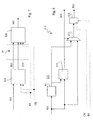
- the variant to the method proposed comprises the following operations, which are illustrated with reference to the flowchart of Figure 6 , where blocks with the same reference numbers execute the same operations as the blocks already illustrated with reference to Figure 5 :
- Figure 7 shows a block diagram representing an encoding circuit 610 and a decoding circuit 620 designed to implement the method described with reference to Figures 5 and 6 .
- the encoding circuit 610 receives at input the non-encoded sequence of input data b(t), the clock signal CK, and a reset signal RS, and supplies at output the encoded sequence B(t) and the inversion signal INV, which are transmitted on the optical bus 16 and reach the decoding circuit 620, which is designed to carry out decoding of the encoded sequence B(t) and supply the non-encoded sequence b(t). On said optical bus 16 there are also sent the clock signal CK and the reset signal RS to the decoding circuit 620.
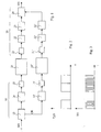
- Figure 8 illustrates a block diagram that shows in detail the encoding circuit 610.
- the non-encoded sequence of input data b(t) is sent at input to a block 611, which represents an inversion module and supplies at output an inverted sequence b (t), i.e., a sequence in which the bits subsequent to the marker bit M are inverted.
- the sequence of input data b(t) is sent in parallel to a comparison block 612. If the number of ones of the sequence b(t) after the marker M is greater than M/2, then the comparison block 612 generates at output an inversion signal INV with value one. Otherwise, this inversion signal INV is zero.
- the comparison block 612 can generate at output an inversion signal INV with value one whenever the number of ones in the sequence b(t) is greater than the number of ones of the inverted sequence b (t). Otherwise, said inversion signal INV is zero.
- the inverted sequence b (t) at output from block 611 and the non-encoded sequence b(t) are moreover sent at input to a multiplexer 613, the selection signal of which is provided by the inversion signal INV. If the number of ones is smaller than M/2, the inversion signal INV is 0, and at output from the multiplexer 613 there is the non-encoded sequence of input data b(t), whilst, if the number of ones is greater than M/2, the inversion signal INV is 1, and at output from the multiplexer 613 there is the inverted sequence b (t).
- the output of the multiplexer 613 is then sent to a register 614, controlled by the clock signal CK and by the reset signal RS, which supplies at output the encoded sequence B(t), timed according to the clock signal CK.
- Figure 9 illustrates in detail the inversion circuit 611, which receives at input the n bits b i (t) of the sequence of input data b(t).
- the most significant bit b n-1 (t) is sent in any case to the output of the circuit 611.
- the most significant bit b n-1 (t) is likewise sent at input to a XOR gate 617, which receives on its other input the next most significant bit b n-2 (t).
- the value of the next most significant bit b n-2 (t) is in any case inverted at the output of the XOR gate 617, thus constituting the inverted bit b n-2 (t) of the inverted sequence b (t).
- the bits b n-1 (t)and b n-2 (t) are sent in parallel at input to an OR logic gate 616, and the output of said OR logic gate 616 is used as input for a further XOR logic gate 617, which executes the XOR logic operation with the bit b n-3 (t).
- the XOR gate 617 inverts the value of the bit b n-3 (t), thus constituting the inverted bit b n-3 (t) of the inverted sequence b (t).
- This logic structure comprising the XOR gate 617 and the OR gate 616, is repeated for all of the bits composing the sequence of input data b(t).
- the effect of this logic structure is that the first bit of the non-encoded sequence of input data b(t) which assumes the value 1, in this way becoming the marker bit M, brings about inversion of all the subsequent less significant bits.
- the method proposed for transmitting a flow of input data on an optical bus of a telecommunications system reduces the power dissipated, in so far as it is possible to transmit a greater number of zeroes as compared to the case of non-encoded data, via identification of the marker bit.
- the method proposed for transmitting a flow of input data on an optical bus of a telecommunications system can advantageously be applied also to the case of serial transmission for minimizing the number of ones.
- the method proposed can advantageously be applied by starting the operation of identification of the marker from the least significant bit, instead of from the most significant bit. Likewise, it is possible to start both from the least significant bit and from the most significant bit and proceed towards the bits within the datum. It is moreover clear that the method proposed can be applied starting from any other bit, for example from the central bit, and proceeding to the left or to the right, or else again in both directions.
Landscapes
- Physics & Mathematics (AREA)
- Engineering & Computer Science (AREA)
- Computer Networks & Wireless Communication (AREA)
- Signal Processing (AREA)
- Electromagnetism (AREA)
- Optics & Photonics (AREA)
- Spectroscopy & Molecular Physics (AREA)
- Dc Digital Transmission (AREA)
- Optical Communication System (AREA)
Claims (13)
- Verfahren zum Übertragen einer Sequenz von Eingabedaten (b(t)) mit ersten ("1") und zweiten Logikzuständen ("0") auf einer optischen Verbindung (16), wobei das Verfahren die Bereitstellung einer optischen Quelle (15) zum Erzeugen eines optischen Signals beinhaltet, das auf der optischen Verbindung (16) zu übertragen ist, wobei die optische Quelle (15) in der Lage ist, optische Impulse beim Auftreten der ersten Logikzustände ("1") zu erzeugen,
wobei das Verfahren folgende Vorgänge aufweist:- Codieren (470; 570) der Sequenz von Eingabedaten (b(t)) in eine codierte Sequenz von Daten (B(t)) vor der Übertragung auf der optischen Verbindung (16), wobei der Codiervorgang (470; 570) die ersten Logikzustände ("1") in der codierten Sequenz von Daten (B(t)) minimiert; und- Ansteuern der optischen Quelle (15) mittels der codierten Sequenz von Daten (B(t)), bei der die Anzahl der ersten Logikzustände ("1") minimiert worden ist, wobei der Codiervorgang (470, 570) ferner folgende Vorgänge aufweist:- Anordnen der Sequenz von Eingabedaten (b(t)) in einem parallelen Format auf einer Anzahl von Leitungen (n; M);- Zählen der ersten Logikzustände ("1") in der Sequenz von Eingabedaten (b(t)) auf der Anzahl von Leitungen (n; M) pro Zeiteinheit;- Vergleichen des Resultats der Zählung mit einem Wert (n/2; M/2), der proportional zu der Anzahl von Busleitungen ist; und- logisches Invertieren der Sequenz von Eingabedaten (b(t)) auf der Anzahl (n) von Leitungen, wenn das Resultat der Zählung größer ist als der Wert (n/2; M/2), der proportional zu der Anzahl von Busleitungen der Sequenz von Eingabedaten (b(t)) ist;dadurch gekennzeichnet,
dass das Verfahren ferner folgende Vorgänge aufweist:- Ordnen (410) der Werte (bi(t)), die die Sequenz von Eingabedaten (b(t)) auf der Anzahl von Busleitungen (n; M) annimmt;- unter den geordneten Werten (bi(t)) erfolgendes Identifizieren (440; 440, 510) des ersten Werts (M), der den ersten Logikzustand ("1") annimmt; und- Anwenden des Codiervorgangs (470, 570) nur an den codierten Werten (bi(t)) im Anschluss an den ersten Wert (M), der den ersten Logikzustand ("1") annimmt. - Verfahren nach Anspruch 1,
dadurch gekennzeichnet, dass es den Vorgang des Erzeugens eines zusätzlichen Signals (INV) aufweist, das auf die optische Verbindung (16) zu schicken ist, wobei das zusätzliche Signal (INV) anzeigt, dass ein entsprechender Bereich der Sequenz von Eingabedaten (b(t)) dem Codiervorgang (470, 670) unterzogen worden ist, wenn das Resultat des Zählvorgangs größer ist als der Wert, der zu der Anzahl von Busleitungen (M/2) der Sequenz von Eingabedaten (b(t)) proportional ist. - Verfahren nach Anspruch 1,
dadurch gekennzeichnet, dass es den Vorgang des Erzeugens eines zusätzlichen Signals (INV) aufweist, das auf die optische Verbindung (16) zu schicken ist, wobei das zusätzliche Signal (INV) anzeigt, dass ein entsprechender Bereich der Sequenz von Eingabedaten (b(t)) dem Codiervorgang (470,670) unterzogen worden ist, wenn das Resultat des Zählvorgangs an der Sequenz von Eingabedaten (b(t)) größer ist als ein Resultat des Zählvorgangs, der an der invertierten Sequenz von Eingabedaten (b(t)) ausgeführt wird. - Verfahren nach Anspruch 1 oder Anspruch 2 oder Anspruch 3,
dadurch gekennzeichnet, dass der Vorgang des Ordnens (410) ausgeführt wird, indem die von der Sequenz von Eingabedaten (b (t) auf der Anzahl von Leitungen (n) angenommenen Werte (bi(t)) in eine Reihenfolge gebracht werden, die mit dem signifikantesten Wert (bn-1(t)) beginnt. - Verfahren nach Anspruch 4,
dadurch gekennzeichnet, dass der signifikanteste Wert (bn-1(t)) uncodiert auf die optische Verbindung (16) geschickt (430) wird. - Verfahren nach Anspruch 4 oder 5,
dadurch gekennzeichnet, dass es den Vorgang des Zuordnens von verschiedenen Logikpegeln (0, C1, C2) zu dem zusätzlichen Signal in Abhängigkeit von dem Wert aufweist, der als erster Wert (M) identifiziert (510) wird, welcher den ersten Logikzustand annimmt. - Verfahren nach Anspruch 6,
dadurch gekennzeichnet, dass dann, wenn der signifikanteste Wert (bn-1(t)) als erster Wert (M) identifiziert (510) wird, der den ersten Logikzustand annimmt, ein dem zusätzlichen Signal (INV) entsprechender (C1) Pegel zugeordnet wird. - Verfahren nach einem oder mehreren der vorausgehenden Ansprüche,
dadurch gekennzeichnet, dass es folgende Vorgänge aufweist:- Bereitstellung der Sequenz von Eingabedaten (b(t)) in einem parallelen Format;- Umwandeln der Sequenz von Eingabedaten (b(t)) von dem parallelen Format in ein serielles Format; und- Ansteuern der optischen Quelle (15) unter Verwendung der in das serielle Format umgewandelten Sequenz von Daten. - Verfahren nach einem oder mehreren der vorausgehenden Ansprüche,
dadurch gekennzeichnet, dass es ferner folgende Vorgänge aufweist:- Übertragen des optischen Signals auf der optischen Verbindung (16);- Empfangen (20) des auf der optischen Verbindung (16) übertragenen optischen Signals, um eine empfangene Sequenz von Daten zu erzeugen; und- Decodieren der empfangenen Sequenz von Daten (B(t)) mittels eines Decodiervorgangs, der zu dem Codiervorgang (470; 570) komplementär ist. - Verfahren nach einem oder mehreren der vorausgehenden Ansprüche,
dadurch gekennzeichnet, dass es sich bei den ersten Logikzuständen ("1") um logische Einsen handelt, die einer Übertragung von optischer Leistung auf der optischen Verbindung zugeordnet sind. - Verfahren nach einem oder mehreren der vorausgehenden Ansprüche,
dadurch gekennzeichnet, dass der zu der Anzahl von Busleitungen (n/2) proportionale Wert gleich der Hälfte (M/2) von Busleitungen ist, die im Anschluss an den ersten Wert (M), der den ersten Logikzustand ("1") annimmt, den geordneten Werten (bi(t)) entsprechen. - System zum Übertragen einer Sequenz von Daten (b(t)) mit ersten ("1") und zweiten Logikzuständen ("0") auf einer optischen Verbindung (16), wobei das System eine optische Quelle (15) zum Erzeugen eines optischen Signals aufweist, das auf der optischen Verbindung (16) zu übertragen ist,
wobei die optische Quelle (15) dazu ausgebldet ist, optische Impulse beim Auftreten der ersten Logikzustände ("1") zu erzeugen,
wobei das System ein Codiermodul (110; 610) zum Codieren der Sequenz von Eingabedaten (b(t)) in eine codierte Sequenz von Daten (B(t)) vor der Übertragung auf der optischen Verbindung (16) aufweist, wobei das Codiermodul (110; 610) dazu konfiguriert ist, die ersten Logikzustände ("1") in der codierten Sequenz von Daten (B(t)) zu minimieren; wobei das Codiermodul (110; 610) für folgende Vorgänge konfiguriert ist:- Zählen der ersten Logikzustände in der Sequenz von Eingabedaten (b(t)), die in einem parallelen Format auf einer Anzahl von Busleitungen (n; M) vorhanden sind;- Vergleichen des Resultats der Zählung mit einem Wert (n/2; M/2), der die Hälfte der Anzahl von Busleitungen (n; M) beträgt; und- logisches Invertieren der Sequenz von Eingabedaten (b(t)) auf der Anzahl von Busleitungen (n; M), wenn das Resultat der Zählung größer ist als der Wert, der die Hälfte der Leitungen (n/2; M/2) der Sequenz von Eingabedaten (b(t)) darstellt,dadurch gekennzeichnet,
dass das Codiermodul (610) ferner für folgende Vorgänge konfiguriert ist:- Ordnen der Werte (bi(t)), die die Sequenz von Eingabedaten (b(t)) auf den Leitungen annimmt;- unter den geordneten Werten erfolgendes Identifizieren des ersten Werts (M), der den ersten Logikzustand ("1") annimmt; und- Anwenden des Codiervorgangs nur an den geordneten Werten (bi(t)) im Anschluss an den ersten Wert (W), der den ersten Logikzustand ("1") annimmt,wobei das Codiermodul (610) aufweist:- ein Inversionsmodul (611) mit einem Netzwerk aus Logikgattern, wie exklusiven ODER-Gattern (617) und ODER-Gatern (616), wobei das Netzwerk zum Ausführen von folgenden Vorgängen ausgebildet ist:a) Ausführen des Vorgangs zum Ordnen der Werte (bi(t)), die die Sequenz von Eingabedaten (b(t)) auf den Leitungen annimmt;b) Ausführen der Identifizierung des ersten Werts (M), der den ersten Logikzustand annimmt, unter den geordneten Werten; undc) logisches Invertieren (b (t)) der Sequenz von geordneten Daten (bi(t)) im Anschluss an den ersten Wert (M), der den ersten Logikzustand annimmt;- einen Vergleichsblock (612) mit einer Einrichtung zum:a) Ausführen des Zählvorgangs der ersten Logikzustände in der Sequenz der geordneten Daten (bi(t)) im Anschluss an den ersten Wert (M), der den ersten Logikzustand annimmt;b) Ausführen des Vorgangs zum Vergleichen des Resultats der Zählung mit einem Wert (n/2; M/2), der die Hälfte der Anzahl von Busleitungen beträgt; undc) Erzeugen eines zusätzlichen Signals (INV), das anzeigt, ob das Resultat des Zählvorgangs größer ist als der Wert (n/2; M/2), der die Hälfte der Anzahl von Busleitungen beträgt;- einen Multiplexer (613), der dazu ausgebildet ist, die codierte Sequenz (B(t)) zwischen der invertierten Sequenz (b (t)) und der Sequenz der Eingabedaten (b(t)) unter der Steuerung des zusätzlichen Signals (INV) auszuwählen. - Computerprogramm-Produkt, das sich direkt in den Speicher eines Computers laden lässt und Software-Codebereiche zum Ausführen des Verfahrens nach einem der Ansprüche 1 bis 11 aufweist, wenn das Produkt auf einem Computer läuft.
Priority Applications (3)
| Application Number | Priority Date | Filing Date | Title |
|---|---|---|---|
| EP03425663A EP1524810B1 (de) | 2003-10-13 | 2003-10-13 | Übertragungsverfahren für eine optische Busleitung |
| DE60322540T DE60322540D1 (de) | 2003-10-13 | 2003-10-13 | Übertragungsverfahren für eine optische Busleitung |
| US10/963,737 US7352301B2 (en) | 2003-10-13 | 2004-10-12 | Method for transmitting a data flow over an optical bus, corresponding system and computer program product |
Applications Claiming Priority (1)
| Application Number | Priority Date | Filing Date | Title |
|---|---|---|---|
| EP03425663A EP1524810B1 (de) | 2003-10-13 | 2003-10-13 | Übertragungsverfahren für eine optische Busleitung |
Publications (2)
| Publication Number | Publication Date |
|---|---|
| EP1524810A1 EP1524810A1 (de) | 2005-04-20 |
| EP1524810B1 true EP1524810B1 (de) | 2008-07-30 |
Family
ID=34354644
Family Applications (1)
| Application Number | Title | Priority Date | Filing Date |
|---|---|---|---|
| EP03425663A Expired - Lifetime EP1524810B1 (de) | 2003-10-13 | 2003-10-13 | Übertragungsverfahren für eine optische Busleitung |
Country Status (3)
| Country | Link |
|---|---|
| US (1) | US7352301B2 (de) |
| EP (1) | EP1524810B1 (de) |
| DE (1) | DE60322540D1 (de) |
Families Citing this family (8)
| Publication number | Priority date | Publication date | Assignee | Title |
|---|---|---|---|---|
| KR100763533B1 (ko) * | 2006-06-01 | 2007-10-05 | 삼성전자주식회사 | 버스 인버팅 코드 생성 장치 및 이를 이용한 버스 인버팅코드 생성 방법 |
| KR101430168B1 (ko) * | 2008-01-09 | 2014-08-13 | 삼성전자주식회사 | 3단계 신호를 송수신하는 광 송수신 장치 |
| IT1394632B1 (it) * | 2009-06-22 | 2012-07-05 | St Microelectronics Srl | "trasmettitore ottico" |
| US8401388B2 (en) | 2009-06-22 | 2013-03-19 | Stmicroelectronics S.R.L. | Optical transmitter |
| US8867925B2 (en) * | 2012-07-20 | 2014-10-21 | Hewlett-Packard Development Company, L.P. | Reducing electrical current of a signal driver for an optical transmitter |
| KR102238176B1 (ko) * | 2014-04-16 | 2021-04-12 | 삼성전자주식회사 | 단일 와이어 프로토콜 통신에서의 데이터 통신 방법 및 그에 따른 단일 와이어 프로토콜 통신 시스템 |
| US9735778B1 (en) * | 2014-08-20 | 2017-08-15 | Altera Corporation | Method and apparatuses for optimizing power management on an integrated circuit device |
| US10956432B2 (en) * | 2017-08-30 | 2021-03-23 | Gsi Technology Inc. | One by one selection of items of a set |
Family Cites Families (6)
| Publication number | Priority date | Publication date | Assignee | Title |
|---|---|---|---|---|
| US4399563A (en) * | 1978-04-18 | 1983-08-16 | Honeywell Information Systems Inc. | Fiber optics high speed modem |
| FR2570905B1 (fr) * | 1984-05-23 | 1987-01-09 | Cit Alcatel | Procede de transmission synchrone de donnees et dispositif pour sa mise en oeuvre |
| US4903338A (en) * | 1986-11-17 | 1990-02-20 | Amp Incorporated | Optical interface |
| US5644601A (en) * | 1994-10-31 | 1997-07-01 | Symbol Technologies, Inc. | Method and apparatus for bias suppression in a VCO based FM transmission system |
| KR100323585B1 (ko) * | 1998-08-31 | 2002-10-25 | 한국전기통신공사 | 오프레벨 샘플링에 의한 전기광학광변조기의 바이어스 안정화방법 |
| AU2003223687A1 (en) * | 2002-04-23 | 2003-11-10 | Quellan, Inc. | Combined ask/dpsk modulation system |
-
2003
- 2003-10-13 DE DE60322540T patent/DE60322540D1/de not_active Expired - Lifetime
- 2003-10-13 EP EP03425663A patent/EP1524810B1/de not_active Expired - Lifetime
-
2004
- 2004-10-12 US US10/963,737 patent/US7352301B2/en not_active Expired - Lifetime
Also Published As
| Publication number | Publication date |
|---|---|
| US7352301B2 (en) | 2008-04-01 |
| EP1524810A1 (de) | 2005-04-20 |
| DE60322540D1 (de) | 2008-09-11 |
| US20050281562A1 (en) | 2005-12-22 |
Similar Documents
| Publication | Publication Date | Title |
|---|---|---|
| EP0150072B1 (de) | Dekodierschaltung | |
| US10122561B2 (en) | Orthogonal differential vector signaling codes with embedded clock | |
| EP1830531B1 (de) | Vorkodierungsschaltung und Vorkodierungs-Multiplexing-Schaltung zur Realisierung sehr hoher Übertragungsraten in einer Lichtwellenleiterkommunikation | |
| EP1524810B1 (de) | Übertragungsverfahren für eine optische Busleitung | |
| CA2278534C (en) | Encoder and decoder | |
| EP0276641A2 (de) | Datenkodierungsschnittstelle | |
| EP0063886B1 (de) | Verfahren und System zur Pulsübertragung | |
| EP0464457B1 (de) | Übertragungsverfahren für optische Busleitung und sendeseitiger Kodierer und empfangsseitiger Dekodierer dafür | |
| JP2005102221A (ja) | プリコーダ及びこれを利用した光デュオバイナリー伝送装置 | |
| EP0151430A2 (de) | Detektor | |
| EP1475906B1 (de) | Verfahren zum übermitteln von Datenströmen über optischen Verbindungen, System und Computerprogramprodukte | |
| US7039323B2 (en) | Optical transmitter for transmitting a plurality of output signals | |
| US6246348B1 (en) | Device for converting multiple signal types to NRZ format with automatic self-test | |
| EP4148531A1 (de) | Taktkonfigurationssystem und -verfahren | |
| EP3382908A1 (de) | Verfahren und vorrichtung zur datenverarbeitung mit mehreren raten | |
| US11398831B2 (en) | Temporal link encoding | |
| JP2668968B2 (ja) | フレーム同期方式 | |
| KR0179579B1 (ko) | 전동차의 광신호 전송회로 | |
| CN101882963B (zh) | 一种多幅度数字脉冲间隔调制装置 | |
| Kayiran et al. | Temporal link encoding | |
| JP2668967B2 (ja) | フレーム同期方式 | |
| JPS58151753A (ja) | パルス通信方式 | |
| Gonzalez-Marcos et al. | Coder/decoder with an optical programmable logic cell | |
| JPH0233246A (ja) | ディジタル信号伝送方式 | |
| KR100249775B1 (ko) | 광 패킷 스위치를 위한 완전 광 헤더 구조 및검출방법 |
Legal Events
| Date | Code | Title | Description |
|---|---|---|---|
| PUAI | Public reference made under article 153(3) epc to a published international application that has entered the european phase |
Free format text: ORIGINAL CODE: 0009012 |
|
| AK | Designated contracting states |
Kind code of ref document: A1 Designated state(s): AT BE BG CH CY CZ DE DK EE ES FI FR GB GR HU IE IT LI LU MC NL PT RO SE SI SK TR |
|
| AX | Request for extension of the european patent |
Extension state: AL LT LV MK |
|
| 17P | Request for examination filed |
Effective date: 20050621 |
|
| AKX | Designation fees paid |
Designated state(s): DE FR GB IT |
|
| 17Q | First examination report despatched |
Effective date: 20061212 |
|
| GRAP | Despatch of communication of intention to grant a patent |
Free format text: ORIGINAL CODE: EPIDOSNIGR1 |
|
| GRAS | Grant fee paid |
Free format text: ORIGINAL CODE: EPIDOSNIGR3 |
|
| GRAA | (expected) grant |
Free format text: ORIGINAL CODE: 0009210 |
|
| AK | Designated contracting states |
Kind code of ref document: B1 Designated state(s): DE FR GB IT |
|
| REG | Reference to a national code |
Ref country code: GB Ref legal event code: FG4D |
|
| REF | Corresponds to: |
Ref document number: 60322540 Country of ref document: DE Date of ref document: 20080911 Kind code of ref document: P |
|
| PLBE | No opposition filed within time limit |
Free format text: ORIGINAL CODE: 0009261 |
|
| STAA | Information on the status of an ep patent application or granted ep patent |
Free format text: STATUS: NO OPPOSITION FILED WITHIN TIME LIMIT |
|
| GBPC | Gb: european patent ceased through non-payment of renewal fee |
Effective date: 20081030 |
|
| 26N | No opposition filed |
Effective date: 20090506 |
|
| REG | Reference to a national code |
Ref country code: FR Ref legal event code: ST Effective date: 20090630 |
|
| PG25 | Lapsed in a contracting state [announced via postgrant information from national office to epo] |
Ref country code: IT Free format text: LAPSE BECAUSE OF FAILURE TO SUBMIT A TRANSLATION OF THE DESCRIPTION OR TO PAY THE FEE WITHIN THE PRESCRIBED TIME-LIMIT Effective date: 20080730 |
|
| PG25 | Lapsed in a contracting state [announced via postgrant information from national office to epo] |
Ref country code: FR Free format text: LAPSE BECAUSE OF NON-PAYMENT OF DUE FEES Effective date: 20081031 |
|
| PG25 | Lapsed in a contracting state [announced via postgrant information from national office to epo] |
Ref country code: GB Free format text: LAPSE BECAUSE OF NON-PAYMENT OF DUE FEES Effective date: 20081030 |
|
| REG | Reference to a national code |
Ref country code: DE Ref legal event code: R082 Ref document number: 60322540 Country of ref document: DE Representative=s name: SCHMITT-NILSON SCHRAUD WAIBEL WOHLFROM PATENTA, DE |
|
| PGFP | Annual fee paid to national office [announced via postgrant information from national office to epo] |
Ref country code: DE Payment date: 20220920 Year of fee payment: 20 |
|
| REG | Reference to a national code |
Ref country code: DE Ref legal event code: R071 Ref document number: 60322540 Country of ref document: DE |