EP1524786A2 - Optoelektronischer Transceiver für eine bidirektionale optische Signalübertragung - Google Patents
Optoelektronischer Transceiver für eine bidirektionale optische Signalübertragung Download PDFInfo
- Publication number
- EP1524786A2 EP1524786A2 EP04077681A EP04077681A EP1524786A2 EP 1524786 A2 EP1524786 A2 EP 1524786A2 EP 04077681 A EP04077681 A EP 04077681A EP 04077681 A EP04077681 A EP 04077681A EP 1524786 A2 EP1524786 A2 EP 1524786A2
- Authority
- EP
- European Patent Office
- Prior art keywords
- wavelength
- light
- carrier substrate
- component
- transceiver according
- Prior art date
- Legal status (The legal status is an assumption and is not a legal conclusion. Google has not performed a legal analysis and makes no representation as to the accuracy of the status listed.)
- Granted
Links
Images



Classifications
-
- H—ELECTRICITY
- H04—ELECTRIC COMMUNICATION TECHNIQUE
- H04B—TRANSMISSION
- H04B10/00—Transmission systems employing electromagnetic waves other than radio-waves, e.g. infrared, visible or ultraviolet light, or employing corpuscular radiation, e.g. quantum communication
- H04B10/40—Transceivers
-
- G—PHYSICS
- G02—OPTICS
- G02B—OPTICAL ELEMENTS, SYSTEMS OR APPARATUS
- G02B6/00—Light guides; Structural details of arrangements comprising light guides and other optical elements, e.g. couplings
- G02B6/24—Coupling light guides
- G02B6/42—Coupling light guides with opto-electronic elements
- G02B6/4201—Packages, e.g. shape, construction, internal or external details
- G02B6/4246—Bidirectionally operating package structures
-
- G—PHYSICS
- G02—OPTICS
- G02B—OPTICAL ELEMENTS, SYSTEMS OR APPARATUS
- G02B6/00—Light guides; Structural details of arrangements comprising light guides and other optical elements, e.g. couplings
- G02B6/24—Coupling light guides
- G02B6/42—Coupling light guides with opto-electronic elements
- G02B6/4292—Coupling light guides with opto-electronic elements the light guide being disconnectable from the opto-electronic element, e.g. mutually self aligning arrangements
Definitions
- the invention relates to an optoelectronic transceiver for bidirectional optical signal transmission.
- SFF small-form-factor
- SFP small form factor pluggable
- SFF transceivers Small design known in a housing are arranged.
- the transceivers can be pluggable formed (SFP transceiver) or fixed to a housing be connected (SFF transceiver).
- the well-known transceivers have in addition to an optoelectronic transmission module and a optoelectronic receive block an internal, parallel to the optical axis of the transceiver extending circuit board on, the electronic circuits for the converter modules contains as a driver block and / or a Preamplifier module.
- the transceiver is on one Main circuit board arranged, for example, over a plug electrically with an electrical interface the internal circuit board is connected.
- An SFP transceiver is described for example in DE 101 14 143 A1.
- EP-A-0 463 214 discloses a transmission and communication module known as a BIDI module Receiving module for a bidirectional optical Signal transmission described.
- the two active components namely light emitter and Light receiver as independent components hermetically sealed encapsulated in a common module housing, in the interior of which is a beam splitter and lens coupling optics are arranged.
- the module housing has a fiber connection for a common optical fiber.
- By the transmitter is an optical signal in the coupled fiber coupled while at the same time another optical Signal from the same fiber can be received.
- the Separation of the two signals is done by a Beam splitter, which also has a wavelength-selective filter which reflects a certain wavelength and lets through a different wavelength.
- WO 02/095470 A1 is an electro-optical module for Transmission and / or reception of optical signals of at least two optical data channels known in which at least two Optical fiber sections each having at least one beveled end face are provided.
- the Fiber optic sections are at the tapered End faces positioned axially one behind the other.
- For one certain optical channel is a Lichteinkopplung or Lichtauskopplung on the beveled end face of a Fiber optic section at an angle to the optical Axis of the optical waveguide.
- the end face is for Wavelength separation with a wavelength-selective filter coated.
- a transmission module for an optical Signal transmission known in which a transmitting device a transmitter substrate and a Detection device on a detection device substrate arranged and the transmitter substrate and the detection device substrate with respect to the direction the emitted or received light on each other are arranged.
- the transmitter substrate and / or the Detector substrate are for those of the Transmitting device emitted wavelength transparent.
- the known transmission module provides an advantageous structure but only one detection device ready.
- transceiver of small design for one Provide bidirectional optical data transmission, the can realize a high data rate and at the same time are inexpensive to produce.
- the solution according to the invention is characterized by the idea out, in a housing of small design with a width of maximum 13.5 mm two bidirectional optical subassemblies to arrange, both for simultaneous sending and Reception of optical signals are suitable.
- an optical Interface for coupling two optical fibers is each subassembly each with an optical fiber optically coupled.
- Each optical subassembly contains both an optical Transmitter as well as an optical receiver. She is also called BOSA (bidirectional optical subassembly). Different as in known transceivers is thus in the present Invention, each subassembly as bidirectional transmitting and Reception module formed. This can be done in an optical Link between two transceivers on an optical fiber simultaneously optical signals in both directions Transfer, with each transfer direction with another Wavelength works. This allows the Transmission capacity of an optical link and thus the Increase the capacity of existing fiber optic networks. simultaneously optical subassemblies of small design are used so that their integration into a housing of small design, in particular according to the SSF or SSP industry standard is possible.
- the Transceiver in addition a multiplexer and a Demultiplexer on. These are preferably in the Transceiver housing integrated, but can basically also be arranged separately.
- the demultiplexer shares one through the transceiver to be transmitted electrical Data stream of a given bandwidth in a first and a second partial data stream to be transmitted in each case one lower bandwidth.
- the first to be transferred Partial data flow is the first sub-assembly and the second to be transferred partial data stream is the second Subassembly supplied.
- the first and second too transferring partial data streams are then via the first and second subassembly emitted as optical signals.
- the Demultiplexer Simultaneously with the transmission of optical signals received first subassembly and the second subassembly one first optical partial data stream to be received and a second partial optical data stream to be received respectively a certain bandwidth, convert this into electrical Signals around and carry the electrical signals to the Multiplexer to, the two received partial data streams to a received electric data stream of a given, higher bandwidth.
- the Demultiplexer a 1: 2 demultiplexer and the multiplexer 2: 1 multiplexer, with the given bandwidths of identical and the received data signal are.
- the The first subassembly has the following components: a Transmitting device, the light of a first wavelength emits; a receiving device, the light of a second Wavelength detected; one for the light of the first Wavelength transparent carrier substrate on which the Transmitting component is arranged; and a monitor component, that is a fraction of the radiated from the transmission component Detected light; wherein the receiving device in the Carrier substrate is integrated; the receiving device and the Transmitting device with respect to the direction of the emitted or received light are arranged one behind the other; the Reception device for the light of the first wavelength optically transparent; and emitted by the transmission component Light the carrier substrate and the receiving device irradiated.
- the second subassembly has the following components: a Transmitting device, the light of a second wavelength emits; a reception component, the light of a first Wavelength detected; one for the light of the first Wavelength and second wavelength transparent Carrier substrate on which the transmission component is arranged; and a monitor component that is a fraction of the Transmitting component emitted light detected; the Reception device and the transmission component with respect to the Direction of the emitted or received light arranged one behind the other; the transmission component for the Light of the first wavelength is optically transparent; from Transmitting component emitted light the carrier substrate irradiated; and the light received by the receiving device the carrier substrate and the transmission component irradiated.
- the two subassemblies are suitable for each other via an optical link simultaneously in both directions Transferring data from one sub-assembly emitted light from the other sub-assembly Will be received.
- bidirectional Subassembly It will each be a compact construction of a bidirectional Subassembly with reduced number of parts and thus low Cost of production provided, the Subassembly at the same time a montoring of the light of the Transmission component allowed.
- the thus constructed bidirectional subassembly is also smaller in size Construction executable and can be in a transceiver housing small design can be integrated.
- the wavelengths of the transmission component and the Reception component are preferably chosen so that they conventional wavelengths in optical transmission technology, thus in particular the optical "windows" more common Glass fibers correspond.
- Preferred are for the first and second wavelength wavelength combinations of 850 nm / 1310 nm, 850 nm / 1490 nm or 850 nm / 1550 nm. Also possible is a combination for the first and second Wavelength of 1310 nm / 1550 nm.
- the transceiver according to the invention is also in Combination with differently designed optical subassemblies executable.
- the transmit micromodule and the receive micromodule in relation to the emitted or to be detected Light superimposed and is the first support element the transmit micromodule for the light to be detected transparent.
- the bottom plate of the TO housing has a recess, which serves to receive the receiving micromodule, wherein the Transmitting micromodule is arranged over this on the bottom plate.
- the other subassembly of the transceiver is down to the Circumstance that the other wavelength is emitted and is detected, identically formed.
- This embodiment of the subassemblies takes up cost-effective designs using a TO housing back.
- edge emitting laser diodes be used.
- the subassembly is in turn smaller Designed to run in a transceiver housing small design can be integrated.
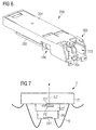
- FIG. 6 shows an optoelectronic transceiver 200 Small design according to the industry standard SFP.
- the Transceiver 200 has an elongated housing 201 with a Width smaller than 13.5 mm.
- the transceiver 200 includes in the housing 201 two juxtaposed bidirectional optical subassemblies (BOSAs) 100, from one is shown.
- An optical interface will be by a plug region 205 with two optical ports 203, 204 provided.
- In each optical port 203, 204 is a Fiber optic plugged, wherein an optical coupling between the optical fiber and the respective Subassembly 100 is made so that each subassembly 100 via a connected optical fiber optical signals send and receive.
- the two subassemblies 100 are for example via a Flex conductor electrically with an internal circuit board 202 of the Transceivers 200 connected in the usual way electrical Components such as a driver block has.
- the Printed circuit board 202 is via an electrical interface (not shown) with a main circuit board connectable. It is conceivable that on the internal Printed circuit board 202 of the transceiver is omitted and the corresponding electrical components in addition to the Subassemblies 100 are integrated.
- both sub-assemblies 100 are designed as bidirectional modules, the transceiver 200 so at the same time on each port light of a wavelength can send out and receive light of a different wavelength.
- the subassemblies 100 are designed in a small construction, so they side by side in the existing case width of 13.5 mm, with a usually additional one Minimum distance between sub-assemblies 100 complied with must become.
- Embodiments of the embodiment of Subassemblies 100 small construction are below to one in Figures 1 to 5 and the other in the figures 8a, 8b described.
- FIG. 9 shows the functional components of the transceiver 200 closer look.
- Each subassembly 100a, 100b has a laser driver 411, 421, a power monitor 412, 422 with an associated automatic shutdown unit 413, 423, a laser diode 414, 424, a monitor diode 415, 425, a Beam splitter 416, 426, a photodetector 417, 427 and a Receive circuit 418, 428 on.
- the beam splitter 416, 426 an optical waveguide 419, 429 is coupled, in which it is preferably is a singlemode optical fiber.
- the mode of operation is known per se.
- the laser diode 414, 424 is driven by the laser driver 411, 421, which with a digital signal to be transmitted at its inputs TD-, TD + is applied.
- Part of the of the laser diode 414, 424 radiation emitted by the monitor diode 415, 425 and the power monitor 412, 422, which corresponds to the determined laser power sends a control signal to the laser driver 411, 421.
- Tx dis Transmit disable
- the light emitted by the laser 4141, 424 is transmitted via the Beam splitter 416, 426 in the optical fiber 419, 429th coupled. On the optical fiber 419, 429 becomes light transmitted bidirectionally.
- Light of one to be detected Wavelength which is different from the wavelength of the emitted Light of the laser 414, 424 differs, is about the Optical fiber 419, 429 received and from the beam splitter 416, 426 the photodetector 417, 427 supplied. That detected Signal is processed in the receiving circuit 418, 428 and at outputs RD-, RD + as regenerated electrical signal output.
- the output "SD" (Signal Detect) indicates whether a received signal is present.
- An external control signal Tx dis can about a unit 430 simultaneously two subassemblies 100a, 100b are supplied, so that if necessary both Laser shut off simultaneously.
- the arrangement of Figure 9 is characterized in that in a bidirectional transceiver both sub-assemblies 100a, 100b as bidirectional units with both a laser 414, 424 and with a detector 417, 427 are executed.
- the Transceiver with the subassembly assemblies 100a, 100b can with a structurally identical transceiver (at the other end of the Optical fibers 419, 429) communicate.
- the laser 414 of Sub-assembly 100a light of a wavelength of 1300 nm emitted while the photodiode 417 light of a wavelength of 850 nm.
- the subassembly 100b sends against it Light of a wavelength of 850 nm and receives light a wavelength of 1300 nm.
- the respective subassembly 100a, 100b can accordingly with her opposite subassembly 100b, 100a of the same communicate with trained transceivers.
- the wavelength combinations are almost arbitrary selectable. Preference is given to wavelength combinations of 850nm / 1310nm, 850nm / 1490nm, 850nm / 1550nm or even 1310/1550 nm selected. From the chosen Wavelength combination depends among other things, whether a Signal transmission between two transceivers via single-mode or multi-mode fibers.
- the arrangement of FIG. 9 is further characterized an additional demultiplexer 440 and multiplexer 450.
- the demultiplexer 440 is a 1: 2 demultiplexer and the Multiplexer 450 a 2: 1 multiplexer.
- the transmission capacity per fiber pair 419, 429 will be doubled.
- the data to be transferred a predetermined bandwidth are provided by the demultiplexer 440 divided into two partial data streams, each half Have bandwidth of the transmitted bandwidth.
- the data of the two partial data streams are each via a Subassembly 100a, 100b and the associated optical fiber 419, 429 transmitted to a similar transceiver. At the same time are from such a similar transceiver transmitted partial data streams from the subassemblies 100a, 100b and supplied to the multiplexer 450.
- Multiplexer 450 By doing Multiplexer 450, the partial data streams to a received electrical data stream with the double, composed of original bandwidth. In this way a bandwidth of data transmission can be realized which is twice the bandwidth of a single one Laser component or receiving component.
- the data stream to be transmitted in two Partial data streams each with a bandwidth of 50% of the split data stream.
- the two Partial data streams are sent to the two in the transceiver 200 arranged optoelectronic subassemblies 100a, 100b passed and converted into optical signals.
- the data stream is therefore divided into two transmission components and - respectively with half the bandwidth - over two at the same time connected optical fibers to a corresponding transferred built transceiver.
- the other one Transceivers are the two data streams over a Multiplexer merged again, making a total of one Data transmission with a double bandwidth compared to each by a transmitter and a receiver provided bandwidth is possible.
- FIG. 1 shows an arrangement with two modules 1, 2 for a bidirectional data transmission.
- the modules are insofar as complementary to each other, as that of the first module 1 emitted light of a first wavelength of the second module 2 detected and that of the second module 2 emitted light of a second wavelength from the first Module 1 is detected.
- a signal transmission section L in which the Signals usually via fiber optics or others Fiber optic cables are transmitted.
- a Transmission via a multimode waveguide Preferably, a Transmission via a multimode waveguide.
- the first module 1 has a carrier substrate 11, a Transmitting device 12, a monitor diode 13 and a Receiving device 14 on.
- the transmitting device 12 it is preferably a VCSEL laser diode with VCSEL structure 121, which formed in a prefabricated chip is.
- the laser diode 12 is upside-down, so with the light-emitting side down on the carrier substrate 11th mounted so that the light-emitting portion 121 immediately adjacent to the carrier substrate 11.
- a monitor diode thirteenth On the back of the laser diode 12 is a monitor diode thirteenth arranged with a photosensitive pn junction 131, the is contacted via bonding wires.
- the monitor diode 13 detects a fraction of that of the laser diode 12 emitted light. It is with a control / regulation device (not shown) for the regulation of Output power of the laser diode 1 connected.
- the monitor diode 13 is also preferred as prefabricated chip formed, preferably in an InP substrate. Alternatively, however, the monitor diode can also monolithically integrated into the laser diode 12. For this Case is on the side facing away from the carrier substrate 11 a pn junction integrated into the laser diode 12 and about about Bonded wires contacted.
- the laser diode 12 transmits light of a first wavelength ⁇ 1 from, wherein ⁇ 1 preferably at about 1310 nm, alternatively at about 1490 nm or about 1550 nm. A fraction of the light is in the direction of the monitor diode 13 from the resonator Laser diode 12 coupled and from the monitor diode 13 to Monitor purposes detected.
- the substrate of the laser diode 12 is for the emitted light of wavelength ⁇ 1 transparent, as well as the substrate of the monitor diode 13.
- Das Substrate of the laser diode 12 consists for example of GaAs, for light with wavelengths above 950 nm is translucent.
- the carrier substrate 11 is preferably made of silicon. Silicon is for wavelengths above about 1100 nm transparent. However, it can also be a different material than Carrier substrate used for the emitted Wavelength ⁇ 1 is transparent.
- the receiving component 14 is in the carrier substrate 11th integrated.
- the carrier substrate forms on the Transmitting device 12 side facing away from a pn junction.
- the use of silicon as the carrier substrate 11 and as Material of the receiving device 14 is special inexpensive.
- the receiving device 14 detects light of a second Wavelength ⁇ 2, which is smaller than the first wavelength ⁇ 1.
- the carrier substrate 11 is not for the second wavelength ⁇ 2 transparent, allowing optical isolation between the Transmitting device 12 and the receiving device 14 with respect the received light of the wavelength ⁇ 2 is present. That from the laser diode 12 emitted light of wavelength ⁇ 1 on the other hand radiates through the carrier substrate 11 and also the Reception diode 14 undisturbed through.
- the wavelengths 1550 nm and 1310 nm must be selected, the carrier substrate from another Material as silicon exist, because silicon for this Wavelengths is transparent and thus an optical Isolation between the transmission component 12 and the Reception device 14 with respect to the received light of Wavelength ⁇ 2 is no longer present.
- the carrier substrate 11 for this case of InP or sapphire with Germanium layers.
- the complementary module 2 also has a carrier substrate 21, a transmission component 22, a reception component 24 and a monitor diode 23 on.
- the transmitting device is preferably in turn around a VCSEL laser diode 22 with a light emitting Area 221, which emits light of the second wavelength ⁇ 2.
- the laser diode 22 is upside-down as a chip 22 on the Substrate 21 attached.
- the substrate of the laser diode 12 is preferably made of GaAs, which is for light with wavelengths above 950 nm is translucent.
- the Receiving device 24 is arranged, preferably as prefabricated photodiode chip (for example from InP) with a integrated pn junction 241 is formed. A Contacting of the receiving diode 24 takes place via bonding wires 9. The receiving diode detects light of wavelength ⁇ 1.
- the module 2 is complementary to the other module 1.
- the monitor diode 23 is in the module 2 in the Support substrate 21 integrated.
- the monitor diode 23 is located in accordance with FIG. 1, preferably on the laser diode 22 facing side of the carrier substrate 21st
- the carrier substrate 21 is for the laser diode 22 emitted light of wavelength ⁇ 2 transparent, as well for the laser diode 12 of the complementary module. 1 emitted light of wavelength ⁇ 1.
- the substrate of Laser diode 22 itself is only for that of the Receiver diode 204 detected light of wavelength ⁇ 1 transparent, not against the emitted light. From the Resonator of the laser diode 22 in the direction of the receiving diode 24th emitted light is therefore absorbed and disturbs the Receiver diode 24 not.
- the substrate of the laser diode 22 becomes accordingly as a block filter.
- a blocking filter on the Reception diode 24 facing side of the laser diode 22nd additionally be arranged a blocking filter. Additional Blocking filters may also be provided in the module 1.
- the light emitted by the laser diode 22 of the wavelength ⁇ 2 first passes through the monitor diode 23. In this case a small fraction of the emitted light for Monitor detected.
- the undetected portion passes through the carrier substrate 21 and is removed from the module 2 decoupled.
- FIG. 2 shows a somewhat more detailed structure of the module 1 of the figure 1.
- the silicon carrier substrate 11 On the one upper side 115 of the silicon carrier substrate 11, that only optically for light of the emitted wavelength ⁇ 1 is transparent, is in flip-chip mounting the VCSEL laser diode 12 arranged.
- the p- and the n-contact of the Laser diode are on the mounting side, i. the the Carrier substrate 201 facing side arranged.
- the Contacting takes place via corresponding metallizations the top 115 of the carrier substrate 11 (not shown).
- the monitor diode 13 On the laser diode 12 is the back of the monitor diode thirteenth mounted, a fraction X of the light of the laser diode 12th detected.
- the electrical connection of the monitor diode 13 takes place via two bonding wires 9, which are provided with corresponding bond pads are connected on the top of the carrier substrate (not shown).
- the silicon carrier substrate 11 In the silicon carrier substrate 11 are two Vias 111, 112, which in the carrier substrate 101 integrated receive diode 14 contact. With it all electrical contacts on a plane, the Mounting plane through the one top 115 of the Carrier substrate 11 is formed. This way can from the Assembly level 15 then in a simple manner to a leadframe are bonded, as shown in Figure 4 is still shown.
- the second module 2 of FIG. 1 is detailed in FIG shown.
- the carrier substrate 21 is both for light the detected wavelength ⁇ 1 as well as for the light emitted wavelength ⁇ 2 transparent. It is preferred made of sapphire. Sapphire is available for wavelengths between 850 nm and 1550 nm transparent.
- the VCSEL laser diode 22 is in turn by means of flip-chip mounting on the one side 215 of the carrier substrate 21 mounted so that both contacts are on the same side.
- the structure is comparable to that of the laser diode 12 of FIG. 2
- the VCSEL laser diode 22 On the VCSEL laser diode 22 is the back for a other wavelength ⁇ 2 sensitive receiving diode 24 with the pn junction 241 mounted.
- it is a receiving diode made of an InP substrate. She serves the Detection of the light emitted by the module 1 of the Wavelength ⁇ 1 emitted by the complementary module 1 has been.
- the monitor diode 23 Integrated into the sapphire is the monitor diode 23.
- a crystalline silicon layer in the sapphire integrated which provides a pn junction.
- the Monitor diode 23 is preferably on the laser diode 22nd facing side of the support substrate 21 formed. This allows easy contacting of the monitor diode via Contacts on the surface 115 of the carrier substrate.
- FIG. 7 shows an alternative embodiment of the module of Figure 3.
- the monitor diode 23 ' not in the carrier substrate 21, but instead in the laser diode 22 'itself integrated.
- This is a pn junction between the VCSEL structure 221 and the (preferred GaAs existing) substrate of the laser diode integrated.
- the Laser diode 22 ' is somewhat in this embodiment made larger than the receiving diode 24, so that the Possibility of contacting a common contact the laser diode 22 'and the integrated monitor diode 23' via a bonding wire 9, the carrier substrate 21 or alternatively contacted directly with a leadframe.
- the substrate acts Laser diode 22 'as a block filter for in the direction of Reception diode 24 radiated light, after this the Monitor diode 23 'has happened.
- FIG. 4 shows the bidirectional module 1, 2 of the figures 2, 3, 7 as a housed module 10, 20 in a standard housing.
- the carrier substrate 11, 21 may be one on the optical Have axis located lens 6, the emitted or received light for better coupling with a Fiber optic forms.
- the carrier substrate 11, 21 is on a leadframe 3 arranged, which has a central recess. 5 for optical access to the module and the Contacting the module 1, 2 provides. Up to the optical access 5 is the arrangement of module 1, 2 and Leadframe 3 with a non-transparent plastic compound molded.
- Such cases are known per se, for example DE 102 01 102 A1, so that they are not discussed in detail becomes.
- FIG. 5 shows a subassembly 100c with the housing Module 10, 20 of Figure 4 in conjunction with an optical Connector receptacle 8 for receiving an optical waveguide connected.
- a flex conductor 7 with conductor tracks and contact pads for contacting the terminals of the Module 10, 20 provided. Not with the module 10, 20 connected end of the flex conductor 7 is connected to a printed circuit board (not shown) connected.
- modules 1, 2 according to Figures 1 to 3 and 7 in any optical Senders, receivers and transceivers can be done and the Use of such modules 1, 2 Although advantageous, but not necessarily in transceivers according to FIGS. 6 and 9 he follows.
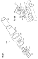
- FIG. 8 shows an alternative embodiment of a Subassembly 100d, which is in an optoelectronic Transceiver 200 according to Figure 6 can be used.
- the subassembly 100d has a TO package, which is in known manner from a bottom plate 310 with Vias for a plurality of contact pins 320 and a cap 330 having an optical window 331, which is hermetically sealed on the bottom plate 310.
- the cap 330 is surrounded by a wall sleeve 340, at whose end face 341 is a cap 350 with a Coupling device 360 for receiving a to be connected Optical waveguide is attached, in which it is preferred is a single-mode optical fiber. It is in the Frame of an active adjustment, the cap 350 in front of a final fixation against the wall sleeve 340 adjusted.
- a structure is for example from WO 98/10319 A1 known.
- the transmit micromodule 370 has as essential components an edge emitting semiconductor laser 371, a 45 ° prism 372 with a monitor diode 373, a beam splitter 374 with a beam-splitting, with a wavelength-selective Filter provided surface 375 and a silicon carrier 376th with an integrated lens 377 on. These components are arranged on a support 378.
- the receiving micromodule 380 has a photodiode 382 on a carrier 381.
- the Transmitting micromodule 370 In the bottom plate 310 of the TO housing is a recess 311, into which the transmitting micromodule 380 is inserted is. Above this, on the surface of the bottom plate 310 is the Transmitting micromodule 370 arranged. The carrier element 378 of the Transmit micromodule is doing for the wavelength, through the photodiode 382 is detected, transparent. Of the Semiconductor laser 371 emitted light is at the beam-splitting surface 375 and reflected by the lens 377th radiated. Received light of a different wavelength on the other hand, the wavelength-selective filter of the beam-splitting surface 375, traverses the support member 387th and is received by the photodiode 382 of the receive micromodule 380 detected. The transmit micromodule 370 and the receive micromodule 380 are respectively via the contact pins 320 and not shown bonding wires contacted.
- the structure described also provides a very compact Way a subassembly with a transmitting and Receiving arrangement ready, with the same light one emitted first wavelength and light a second Wavelength can be detected.
- the TO housing used preferably has external dimensions perpendicular to the optical axis of the exiting laser light of maximum 6.5mm on top, allowing for mounting in Small Form Factor (SFF) transceivers and small form factor pluggable (SFP transceivers) small design is possible.
- SFF Small Form Factor
- SFP transceivers small form factor pluggable
Landscapes
- Physics & Mathematics (AREA)
- Electromagnetism (AREA)
- Engineering & Computer Science (AREA)
- Computer Networks & Wireless Communication (AREA)
- Signal Processing (AREA)
- General Physics & Mathematics (AREA)
- Optics & Photonics (AREA)
- Optical Couplings Of Light Guides (AREA)
- Semiconductor Lasers (AREA)
Abstract
Description
Es zeigen:
- Figur 1 -
- eine schematische Darstellung des Aufbaus zweier einander komplementärer optischer Subbaugruppen für die bidirektionale Datenübertragung,
- Figur 2 -
- den Aufbau einer ersten Subbaugruppe für eine bidirektionale Datenübertragung, die Licht einer ersten Wellenlänge aussendet und Licht einer zweiten Wellenlänge empfängt,
- Figur 3 -
- den Aufbau einer zweiten Subbaugruppe für eine bidirektionale Datenübertragung, die Licht der zweiten Wellenlänge aussendet und Licht der ersten Wellenlänge empfängt,
- Figur 4 -
- einen Schnitt durch ein Gehäuse mit einer Subbaugruppe gemäß den Figuren 2 oder 3,
- Figur 5 -
- eine perspektivische Ansicht der Subbaugruppe der Figur 4, die mit einer Steckeraufnahme verbunden und über eine Flexfolie kontaktiert ist,
- Figur 6 -
- in perspektivischer Darstellung einen optoelektronischen Transceiver mit einem Gehäuse und zwei Subbaugruppen gemäß Figur 5 oder gemäß Figur 8a,
- Figur 7 -
- eine alternative Ausgestaltung der Subbaugruppe der Figur 3,
- Figur 8a -
- in Explosionsdarstellung den Aufbau eines weiteren Ausführungsbeispiels einer Subbaugruppe für einen Transceiver gemäß Figur 6,
- Figur 8b -
- eine Detailansicht der Subbaugruppe der Figur 8a, die die Anordnung eines Mikro-Sendemoduls und eines Mikro-Empfangsmoduls auf der Bodenplatte eines TO-Gehäuses darstellt, und
- Figur 9
- ein Blockdiagramm der funktionalen Komponenten des Transceivers des Figur 6.
Claims (31)
- Optoelektronischer Transceiver für eine bidirektionale optische Signalübertragung miteinem Gehäuse (201) mit einer Breite von maximal 13,5 mm,einer ersten in dem Gehäuse angeordneten bidirektionalen optischen Unterbaugruppe (100; 100a; 100c; 100d) zum gleichzeitigen Aussenden und Empfang optischer Signale,einer zweiten in dem Gehäuse angeordneten bidirektionalen optischen Unterbaugruppe 100; 100b; 100c; 100d) zum gleichzeitigen Aussenden und Empfang optischer Signale, undeiner optischen Schnittstelle (205) zur Ankopplung zweier Lichtwellenleiter, wobei jeweils ein Lichtwellenleiter mit einer Unterbaugruppe (100; 100a, 100b; 100c; 100d) optisch koppelbar ist.
- Transceiver nach Anspruch 1, zusätzlich aufweisend einen Multiplexer (250) und einen Demultiplexer (240), wobeider Demultiplexer (240) einen durch den Transceiver zu übertragenden elektrischen Datenstrom einer vorgegebenen Bandbreite in einen ersten und einen zweiten zu übertragenden Teildatenstrom jeweils einer geringeren Bandbreite aufteilt,der erste zu übertragende Teildatenstrom der ersten Unterbaugruppe und der zweite zu übertragende Teildatenstrom der zweiten Unterbaugruppe zugeführt wird, unddie ersten und zweiten zu übertragenden Teildatenströme über die erste und zweite Unterbaugruppe als optische Signale ausgesandt werden, und wobeidie erste Unterbaugruppe und die zweite Unterbaugruppe gleichzeitig zum Aussenden optischer Signale einen ersten zu empfangenden optischen Teildatenstrom und einen zweiten zu empfangenden optischen Teildatenstrom jeweils einer bestimmten Bandbreite empfangen, in elektrische Signale umwandeln und dem Multiplexer (250) zuführen, der die beiden empfangenen Teildatenströme zu einem emfangenen elektrischen Datenstrom einer vorgegebenen, höheren Bandbreite zusammensetzt.
- Transceiver nach Anspruch 2, wobei der Demultiplexer (240) ein 1:2 Demultiplexer und der Multiplexer (250) ein 2:1 Multiplexer ist und die vorgegebene Bandbreiten des zu übertragenden und des empfangenen Datensignals identisch sind.
- Transceiver nach Anspruch 1, wobei der Multiplexer (250) und der Demultiplexer (240) in den Transceiver (200) integriert sind.
- Transceiver nach Anspruch 1, wobei die erste Unterbaugruppe aufweist:ein Sendebauelement (12), das Licht einer ersten Wellenlänge (λ1) aussendet,ein Empfangsbauelement (14), das Licht einer zweiten Wellenlänge (λ2) detektiert,ein für das Licht der ersten Wellenlänge transparenten Trägersubstrat (11), auf dem das Sendebauelement angeordnet ist, undein Monitorbauelement (13), das einen Bruchteil des vom Sendebauelement (12) ausgestrahlten Lichts detektiert, wobeidas Empfangsbauelement (14) in das Trägersubstrat (11) integriert ist,das Empfangsbauelement (14) und das Sendebauelement (12) in Bezug auf die Richtung des ausgesandten bzw. empfangenen Lichts hintereinander angeordnet sind,das Empfangsbauelement (14) für das Licht der ersten Wellenlänge (λ1) optisch transparent ist undvom Sendebauelement (12) ausgesandtes Licht das Trägersubstrat (11) und das Empfangsbauelement (14) durchstrahlt.
- Transceiver nach Anspruch 5, wobei das Sendebauelement (12) mit der Oberseite nach unten auf dem Trägersubstrat (11) montiert ist.
- Transceiver nach Anspruch 5, wobei das Empfangsbauelement (14) auf der dem Sendebauelement (12) abgewandten Seite des Trägersubstrats (11) in dieses integriert ist.
- Transceiver nach Anspruch 5, wobei das in das Trägersubstrat integrierte Empfangsbauelement (14) einen in das Trägersubstrat integrierten pn-Übergang ausbildet.
- Transceiver nach Anspruch 7, dadurch gekennzeichnet, dass das Trägersubstrat (11) zwei Durchkontaktierungen (111, 112) aufweist, die von der dem Sendebauelement (12) zugewandten Seite (115) des Trägersubstrats (11) ausgehen und das Empfangsbauelement (14) kontaktieren.
- Transceiver nach Anspruch 5, wobei das Trägersubstrat (11) für Licht der zweiten Wellenlänge (λ2) nicht transparent ist.
- Transceiver nach Anspruch 5, wobei die erste Wellenlänge (λ1) größer ist als die zweite Wellenlänge (λ2).
- Transceiver nach Anspruch 11, wobei die erste Wellenlänge (λ1) bei 1310 nm, 1490 nm oder 1550 nm und die zweite Wellenlänge (λ2) bei 850 nm oder 1310 nm liegt.
- Transceiver nach Anspruch 5, wobei das Trägersubstrat (11) aus Silizium besteht.
- Transceiver nach Anspruch 5, wobei das Monitorbauelement (13) auf der dem Trägersubstrat (11) abgewandten Seite des Sendebauelementes (12) angeordnet ist.
- Transceiver nach Anspruch 5, wobei das Sendebauelement als Laserchip (12) und das Monitorbauelement als Monitordioden-Chip (13) ausgebildet sind.
- Transceiver nach Anspruch 5, wobei das Monitorbauelement auf der dem Trägersubstrat abgewandten Seite des Sendebauelementes in dieses integriert ist.
- Transceiver nach Anspruch 1, wobei die zweite Unterbaugruppe aufweist:ein Sendebauelement (22), das Licht einer zweiten Wellenlänge (λ2) aussendet,ein Empfangsbauelement (24), das Licht einer ersten Wellenlänge (λ1) detektiert,ein für das Licht der ersten Wellenlänge (λ1) und der zweiten Wellenlänge (λ2) transparentes Trägersubstrat (21), auf dem das Sendebauelement angeordnet (22) ist, undein Monitorbauelement (23), das einen Bruchteil des vom Sendebauelement (22) ausgestrahlten Lichts detektiert, wobeidas Empfangsbauelement (24) und das Sendebauelement (22) in Bezug auf die Richtung des ausgesandten bzw. empfangenen Lichts hintereinander angeordnet sind,das Sendebauelement (22) für das Licht der ersten Wellenlänge optisch transparent ist,vom Sendebauelement (22) ausgesandtes Licht das Trägersubstrat (21) durchstrahlt unddas vom Empfangsbauelement (24) empfangene Licht das Trägersubstrat (21) und das Sendebauelement (22) durchstrahlt.
- Transceiver nach Anspruch 17, wobei das Monitorbauelement (23) in das Trägersubstrat (21) integriert ist.
- Transceiver nach Anspruch 18, wobei das Monitorbauelement (23) auf der dem Sendebauelement (22) zugewandten Seite des Trägersubstrats (21) in dieses integriert ist.
- Transceiver nach Anspruch 18, wobei das in das Trägersubstrat (21) integrierte Monitorbauelement (23) einen in das Trägersubstrat (21) integrierten pn-Übergang ausbildet.
- Transceiver nach Anspruch 17, wobei das Monitorbauelement (23') in das Sendebauelement (22') integriert ist.
- Transceiver nach Anspruch 17, wobei das Sendebauelement (22) mit der Oberseite nach unten auf dem Trägersubstrat (21) angeordnet ist.
- Transceiver nach Anspruch 17, wobei die photoempfindliche Schicht (241) des Empfangsbauelements (24) auf der dem Sendebauelement (22) abgewandten Seite des Empfangsbauelements (24) angeordnet ist.
- Transceiver nach Anspruch 17, wobei das Substrat des Sendebauelements (22) für das ausgesandte Licht der zweiten Wellenlänge (λ2) nicht transparent ist.
- Transceiver nach Anspruch 17, wobei die erste Wellenlänge (λ1) größer ist als die zweite Wellenlänge (λ2).
- Transceiver nach Anspruch 25, wobei die erste Wellenlänge (λ1) bei 1310 nm, 1490 nm oder 1550 nm und die zweite Wellenlänge (λ2) bei 850 nm oder 1310 nm liegt.
- Transceiver nach Anspruch 17, wobei das Trägersubstrat (21) aus Saphir besteht.
- Transceiver nach Anspruch 17, wobei das Sendebauelement als Laserchip (22) und das Empfangsbauelement als Photodioden-Chip (24) ausgebildet sind.
- Transceiver nach Anspruch 17, wobei das Sendebauelement durch eine vertikal emittierende Laserdiode gebildet ist.
- Transceiver nach Anspruch 1, wobei eine Unterbaugruppe aufweist:ein Sende-Mikromodul (370), das auf einem ersten Trägerelement (378) ein Laserbauelement (371), das Licht einer ersten Wellenlänge emittiert, aufweist,ein Empfangs-Mikromodul (380), das auf einem zweiten Trägerelement (381) eine Fotodiode (382) aufweist, die Licht einer zweiten Wellenlänge detektiert, undein TO-Gehäuse mit einer Bodenplatte (310), die der Anordnung der Sende-Mikromoduls und des Empfangs-Mikromoduls dient, wobeidas Sende-Mikromodul (370) und das Empfangs-Mikromodul (380) in Bezug auf das emittierte bzw. zu detektierende Licht übereinander angeordnet sind, und wobeidas erste Trägerelement (378) des Sende-Mikromoduls (370) für das zu detektierende Licht transparent ist.
- Transceiver nach Anspruch 30, wobei die Bodenplatte (310) des TO-Gehäuses eine Aussparung (311) aufweist, die der Aufnahme des Empfangs-Mikromoduls (380) dient, und das Sende-Mikromodul (370) hierüber auf der Bodenplatte (310) angeordnet ist.
Applications Claiming Priority (4)
| Application Number | Priority Date | Filing Date | Title |
|---|---|---|---|
| DE10348675A DE10348675B3 (de) | 2003-10-15 | 2003-10-15 | Modul für eine bidirektionale optische Signalübertragung |
| DE10348675 | 2003-10-15 | ||
| US769287 | 2004-01-30 | ||
| US10/769,287 US7418208B2 (en) | 2003-10-15 | 2004-01-30 | Optoelectronic transceiver for a bidirectional optical signal transmission |
Publications (3)
| Publication Number | Publication Date |
|---|---|
| EP1524786A2 true EP1524786A2 (de) | 2005-04-20 |
| EP1524786A3 EP1524786A3 (de) | 2005-11-02 |
| EP1524786B1 EP1524786B1 (de) | 2008-09-10 |
Family
ID=34379087
Family Applications (1)
| Application Number | Title | Priority Date | Filing Date |
|---|---|---|---|
| EP20040077681 Expired - Lifetime EP1524786B1 (de) | 2003-10-15 | 2004-09-28 | Optoelektronischer Transceiver für eine bidirektionale optische Signalübertragung |
Country Status (1)
| Country | Link |
|---|---|
| EP (1) | EP1524786B1 (de) |
Cited By (1)
| Publication number | Priority date | Publication date | Assignee | Title |
|---|---|---|---|---|
| CN112865872A (zh) * | 2021-03-06 | 2021-05-28 | 珠海思开达技术有限公司 | 模拟光传输模块 |
Family Cites Families (4)
| Publication number | Priority date | Publication date | Assignee | Title |
|---|---|---|---|---|
| DE4444470A1 (de) * | 1994-11-29 | 1996-05-30 | Hertz Inst Heinrich | Sender/Empfänger-Anordnung für ein optisches Duplexsystem |
| JPH11305078A (ja) * | 1998-04-27 | 1999-11-05 | Oki Electric Ind Co Ltd | 光送受信モジュール |
| DE10064599A1 (de) * | 2000-12-18 | 2002-07-04 | Infineon Technologies Ag | Sende-/Empfangsmodul für eine bidirektionale optische Nachrichten-und Signalübertragung |
| GB2378068B (en) * | 2001-07-27 | 2005-05-04 | Motorola Inc | Bipolar differential amplifier |
-
2004
- 2004-09-28 EP EP20040077681 patent/EP1524786B1/de not_active Expired - Lifetime
Cited By (1)
| Publication number | Priority date | Publication date | Assignee | Title |
|---|---|---|---|---|
| CN112865872A (zh) * | 2021-03-06 | 2021-05-28 | 珠海思开达技术有限公司 | 模拟光传输模块 |
Also Published As
| Publication number | Publication date |
|---|---|
| EP1524786B1 (de) | 2008-09-10 |
| EP1524786A3 (de) | 2005-11-02 |
Similar Documents
| Publication | Publication Date | Title |
|---|---|---|
| DE10348675B3 (de) | Modul für eine bidirektionale optische Signalübertragung | |
| EP0600267B1 (de) | Bidirektionaler optischer Sende- und Empfangsmodul | |
| DE69409204T2 (de) | Optischer, bidirektionaler Übertragungsmodul | |
| EP1311890B1 (de) | Opto-elektronische baugruppe zum multiplexen und/oder demultiplexen optischer signale | |
| DE10105943B4 (de) | Faseroptisches Linsensystem zum Koppeln von Fasern mit oberflächenbefestigten Bauelementen | |
| DE102012200254B4 (de) | Optische Verbindungssysteme mit Stecker, welcher eine optische Biegung hat, und Benutzungsverfahren | |
| DE102004025735B4 (de) | Optischer-Empfänger-Gehäuse und Verfahren zu dessen Herstellung | |
| EP0463214B1 (de) | Sende- und Empfangsmodul für eine bidirektionale optische Nachrichten- und Signalübertragung | |
| DE69620515T2 (de) | Photodioden/Diodenlaser-Baustein und Photodioden-Baustein | |
| EP1425619B1 (de) | Sende- und empfangsanordnung für eine bidirektionale optische datenübertragung | |
| DE60032338T2 (de) | Optische nachrichtenübertragungsvorrichtung | |
| DE69916914T2 (de) | LD/PD Modul und LED/PD Modul | |
| EP3201663B1 (de) | Optoelektronisches bauelement | |
| DE69836058T2 (de) | Mehrkanaliges optisches Empfänger-/Sendersystem | |
| EP0383138A2 (de) | Vorrichtung für den optischen Direktempfang mehrerer Wellenlängen | |
| DE19917596B4 (de) | Bidirektionales optisches Kommunikationsbauteil und bidirektionale optische Kommunikationsvorrichtung | |
| DE102012215517A1 (de) | Ein optisches Kopplungssystem zur Verwendung in einem optischen Kommunikationsmodul, ein optisches Kommunikationsmodul, das das optische Kopplungssystem integriert, und ein Verfahren | |
| EP1379903A1 (de) | Sendemodul für eine optische signalübertragung | |
| DE4444470A1 (de) | Sender/Empfänger-Anordnung für ein optisches Duplexsystem | |
| DE69015588T2 (de) | Optischer Kopf integrierbar in einem hybriden Schaltkreis. | |
| DE60216119T2 (de) | Integrierte arrays von modulatoren und lasern auf einer elektronischen schaltung | |
| DE3782043T2 (de) | Signalquelle fuer optische nachrichtentechnik. | |
| DE60130150T2 (de) | Photonische signalmatrix in integrierter schaltung | |
| EP1524786B1 (de) | Optoelektronischer Transceiver für eine bidirektionale optische Signalübertragung | |
| DE3737251C2 (de) | Halbleiter-Trägerelement für ein elektro-optisches Modul |
Legal Events
| Date | Code | Title | Description |
|---|---|---|---|
| PUAI | Public reference made under article 153(3) epc to a published international application that has entered the european phase |
Free format text: ORIGINAL CODE: 0009012 |
|
| AK | Designated contracting states |
Kind code of ref document: A2 Designated state(s): AT BE BG CH CY CZ DE DK EE ES FI FR GB GR HU IE IT LI LU MC NL PL PT RO SE SI SK TR |
|
| AX | Request for extension of the european patent |
Extension state: AL HR LT LV MK |
|
| PUAL | Search report despatched |
Free format text: ORIGINAL CODE: 0009013 |
|
| AK | Designated contracting states |
Kind code of ref document: A3 Designated state(s): AT BE BG CH CY CZ DE DK EE ES FI FR GB GR HU IE IT LI LU MC NL PL PT RO SE SI SK TR |
|
| AX | Request for extension of the european patent |
Extension state: AL HR LT LV MK |
|
| 17P | Request for examination filed |
Effective date: 20060427 |
|
| AKX | Designation fees paid |
Designated state(s): DE FR GB |
|
| RAP1 | Party data changed (applicant data changed or rights of an application transferred) |
Owner name: FINISAR CORPORATION |
|
| GRAP | Despatch of communication of intention to grant a patent |
Free format text: ORIGINAL CODE: EPIDOSNIGR1 |
|
| GRAS | Grant fee paid |
Free format text: ORIGINAL CODE: EPIDOSNIGR3 |
|
| GRAA | (expected) grant |
Free format text: ORIGINAL CODE: 0009210 |
|
| AK | Designated contracting states |
Kind code of ref document: B1 Designated state(s): DE FR GB |
|
| REG | Reference to a national code |
Ref country code: GB Ref legal event code: FG4D Free format text: NOT ENGLISH |
|
| REF | Corresponds to: |
Ref document number: 502004008013 Country of ref document: DE Date of ref document: 20081023 Kind code of ref document: P |
|
| PLBE | No opposition filed within time limit |
Free format text: ORIGINAL CODE: 0009261 |
|
| STAA | Information on the status of an ep patent application or granted ep patent |
Free format text: STATUS: NO OPPOSITION FILED WITHIN TIME LIMIT |
|
| 26N | No opposition filed |
Effective date: 20090611 |
|
| PG25 | Lapsed in a contracting state [announced via postgrant information from national office to epo] |
Ref country code: DE Free format text: LAPSE BECAUSE OF NON-PAYMENT OF DUE FEES Effective date: 20090401 |
|
| REG | Reference to a national code |
Ref country code: FR Ref legal event code: ST Effective date: 20090731 |
|
| PG25 | Lapsed in a contracting state [announced via postgrant information from national office to epo] |
Ref country code: FR Free format text: LAPSE BECAUSE OF NON-PAYMENT OF DUE FEES Effective date: 20081110 |
|
| PGFP | Annual fee paid to national office [announced via postgrant information from national office to epo] |
Ref country code: GB Payment date: 20140929 Year of fee payment: 11 |
|
| GBPC | Gb: european patent ceased through non-payment of renewal fee |
Effective date: 20150928 |
|
| PG25 | Lapsed in a contracting state [announced via postgrant information from national office to epo] |
Ref country code: GB Free format text: LAPSE BECAUSE OF NON-PAYMENT OF DUE FEES Effective date: 20150928 |