Technical field of the invention
The present invention relates to a method for
fabricating a semiconductor device having a
semiconductor element with at least one connection
region, in which the contact resistance of the at least
one connection region is reduced and in which
unfavourable influences of doping elements are avoided.
Background of the invention
Due to an increase in integration of devices which
comprise, for example, MOSFETs (metal oxide
semiconductor field-effect transistors) and are
fabricated with the aid of MOS or CMOS processes, the
miniaturization of these devices represents an ongoing
challenge. Not only do the dimensions and regions of
the device need to be reduced in size, but also there
continue to be high expectations with regard to quality
and yield. The requirements imposed on the junctions in
devices of this type are related to a very high
activation of the doping, good control of the depth of
the junction, etc. At the same time, contacts with a
low resistance via silicides are required in order to
allow contact via the back surface.
A method for fabricating an IGFET which includes a gate
electrode with a low resistance is known from
US 5,851,891, which describes the fabrication of an
IGFET (insulated gate field-effect transistor) in which
the gate electrode of the IGFET is made from silicon
and a connection region is formed therein by enabling
the silicon to react with a metal applied to it so as
to form a metal silicide. Apart from in the vicinity of
the dielectric region, the silicon of the gate
electrode is doped with doping atoms, such as boron
atoms. When the metal silicide is being formed, these
doping atoms are forced towards the dielectric region
without penetrating through it. On the other hand, the
relatively high doping concentration formed in this way
in the vicinity of the dielectric region ensures that
an undesirable depletion layer effect does not occur in
the gate electrode, since such an effect would increase
the effective thickness of the dielectric region. The
expulsion of doping atoms before the interface of the
silicide which is formed is known as the snowplough
effect.
One drawback of the method described above is that
there is nevertheless still a risk of doping atoms
penetrating into or through the dielectric region,
which is unfavourable for the electrical properties of
the semiconductor element.
Summary of the invention
It is an object of the present invention to provide a
method for fabricating a semiconductor device having at
least one connection region in which the contact
resistance of the connection region is reduced and
unfavourable influences from doping elements are
avoided.
The invention provides a method for fabricating a
semiconductor device comprising a semiconductor
structure having a silicon region forming at least one
connection region in and/or on a substrate having a
surface. The method comprises forming a metal cluster
layer from a first metal over the semiconductor
structure or at least over the silicon region thereof.
This metal cluster layer is formed in such a manner
that in the layer metal clusters alternate with sites
where there are no metal clusters. It is preferable
that a non-siliciding metal, in other words a metal
which is inert with regard to reaction with silicon
under the experimental conditions, such as for example
W, Mo, Ta, Zr or Nb, is selected for the first metal.
Furthermore, the method of the invention comprises the
deposition of a metal layer of a second metal on top of
the metal cluster layer. The second metal is a
siliciding metal and may, for example, be Ti, Co or Ni.
Then, the semiconductor device is subjected to at least
one heat treatment in which metal silicide is formed
through reaction of the second metal with silicon of
the silicon region and in which the atoms of the first
metal are displaced in a direction substantially
perpendicular to the surface of the substrate, and this
as a result of the Kirkendall effect.
The method according to the invention is characterized
in that the metal atoms selected for the atoms of the
first metal are different from the second metal, which
forms a metal silicide with silicon. The metal atoms of
the first metal are introduced into or into the
vicinity of that region of the regions which form metal
silicide whose atoms have the highest diffusion rate
during the formation of the metal silicide.
In one specific embodiment, it is possible to fabricate
a semiconductor device having a substrate and a
semiconductor body made from silicon. The semiconductor
body comprises a semiconductor element having at least
two semiconductor regions and having a pn junction
formed between two of the semiconductor regions which
are of opposite conduction types. The semiconductor
body furthermore comprises at least two electrical
connection regions, at least one connection region
being formed by a metal region being brought into
contact with a silicon region of the semiconductor body
and these regions being allowed to react with one
another to form a metal silicide which forms part of
the connection region, atoms of the metal region and of
the silicon region reacting with one another. Before
the metal silicide is formed, atoms of a material other
than silicon or the metal being applied in one of the
regions which form metal silicide or between them, in
such a manner that these atoms form a region in layer
form with interruptions where there are no atoms of the
other material, and the atoms of the other material
being displaced, during the formation of the metal
silicide, in a direction which is perpendicular to the
interface between the metal region and the silicon
region. The method is characterized in that metal atoms
of another metal are selected for the atoms of the
other material, and the atoms of the other metal are
introduced into or into the vicinity of that region of
the regions which form metal silicide whose atoms have
the highest diffusion rate during the formation of the
metal silicide.
In one embodiment of the invention, the semiconductor
structure may comprise a first main electrode and a
second main electrode and a control electrode. In one
specific embodiment, the first main electrode and
second main electrode can be provided with a connection
region. In another embodiment, the control electrode
may be provided with a connection region. In a
preferred embodiment, both the first and second main
electrodes and the control electrode may be provided
with a connection region fabricated as described in the
invention.
In one specific embodiment of the invention, the
semiconductor structure can be formed as a field-effect
transistor having a source region, a drain region and a
gate electrode, and the source and drain region and/or
gate electrode can be provided with a connection
region.
In one embodiment of the invention, the first metal can
be selected in such a way that its work function is as
close as possible to the value desired for the
transistor. By way of example, if an NMOST is being
formed, the metal selected has a work function which is
as close as possible to the value required for an
NMOST, namely approximately 4.2 eV. The same applies to
a PMOST, in which case a metal with a work function in
the vicinity of approximately 5.2 eV is selected.
In a further embodiment of the invention, a
semiconductor device having at least one NMOS
transistor and at least one PMOS transistor can be
fabricated. In this case, the metal cluster layer of
the NMOST may be formed from a metal which is different
from the metal cluster layer of the PMOST. In this way,
it is then possible to obtain different work functions.
In one specific embodiment of the invention, the atoms
of the first metal can be applied to the silicon region
from the vapour phase in the form of clusters of metal
atoms. In this way, openings or sites where there are
no clusters are incorporated. In another embodiment,
the atoms of the first metal layer may, as an
alternative, be applied by a uniform layer of the first
metal being applied to the silicon region of the
substrate, and the uniform layer can then be provided
with openings. In yet another embodiment of the
invention, the atoms of the first metal can be applied
by means of ion implantation.
Furthermore, the invention provides a semiconductor
device having a silicon region and a semiconductor
structure with a connection region, the semiconductor
device being obtained with the aid of the method of the
present invention.
In one specific embodiment, the semiconductor structure
may comprise a first main electrode, a second main
electrode and a control electrode. In yet another
embodiment, the semiconductor structure may be a field-effect
transistor having a source region, a drain
region and a gate electrode.
Other characteristics, properties and advantages of the
present invention will become apparent from the
following detailed description together with the
appended figures which illustrate the basic principles
of the invention by way of example.
Brief description of the drawings
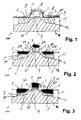
Figures 1 to 3 diagrammatically depict a cross section
through a semiconductor device in successive stages of
the fabrication in accordance with a first embodiment
of a method according to the invention;
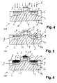
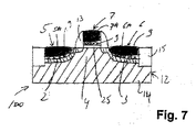
Figures 4 to 7 diagrammatically depict a cross section
through a semiconductor device in successive stages of
the fabrication in accordance with a second embodiment
of a method according to the invention;
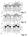
Figures 8 to 13 diagrammatically depict a cross section
through a semiconductor device in successive stages of
the fabrication in accordance with a third embodiment
of a method according to the invention.
Description of illustrative embodiments
The present invention will be described below with the
aid of various embodiments and with reference to a
number of figures. However, the invention is not
restricted to these embodiments and figures. The
figures described are only diagrammatic and are not
intended to constitute any form of restriction. The
dimensions of some elements are exaggerated and not to
scale in the figures in order to illustrate a specific
concept.
The method of the present invention can be used to
fabricate semiconductor structures having a gate
electrode 1 and a source and drain region 2, 3. The
invention is based first of all on the insight that on
account of the presence of metal atoms in the vicinity
of the dielectric region 25 between a substrate 14 and
the gate electrode 1, it is possible, so to speak, to
form a metal-containing gate electrode 1. There is then
no need or scarcely any need to dope the silicon of the
gate electrode 1. Moreover, for example in the case of
a CMOS IC (complementary MOS; contains both n-type and
p-type transistors), by applying a different metal in
the two types of transistors, it is possible to match
the work function thereof to each transistor. The work
function of the gate is, according to the invention,
controlled by the presence of a metal layer in the
border region between the gate electrode 1 and the
dielectric region underneath it (see further).
Furthermore, the invention is based on the insight that
metal atoms can be displaced in silicon in a similar
way to doping atoms, but by a significantly different
mechanism, namely based on the effect named after
Kirkendall. The Kirkendall effect is based on the
displacement of foreign atoms in a reaction matrix as a
result of them being, so to speak, swept through
vacancies which, in a matrix of this type, are subject
to a displacement in the opposite direction to the
direction of the fastest-diffusing component of the
reaction matrix. The snowplough effect, on the other
hand, is based on a differing solubility of doping
atoms in silicon and in metal silicide. Since the
solubility in the metal silicide is much lower than in
silicon, the doping atoms are precipitated out of the
metal silicide and then pass into the remaining silicon
which has not yet reacted. It is important to
understand that this effect originates fro an other
physical process than the Kirkendall effect. It is
caused by the repulsion of the doping atoms by the
growing metal component consequent on a too low
solubility. The doping atoms are thereby, in case of
the snowplough effect, shoved in front of the moving
surface of the metal component.
Figures 1 to 3 diagrammatically depict a cross section
through a semiconductor device 100 in successive stages
of the fabrication in accordance with a first
embodiment of a method according to the invention. Only
the most relevant stages are shown in the drawing. The
starting point for the formation of the device 100 is a
semiconductor body 12 (Fig. 1), which in this
embodiment of the invention may, for example, be formed
from silicon and has a substrate 14, which in this
embodiment may likewise be formed from silicon and in
which a MOSFET is formed, having a source region 2, a
channel region 4 of opposite conduction type to the
source region 2, and a drain region 3 of the same
conduction type as the source region 2. Above the
channel region 4 a dielectric region 25 is formed, for
example, from silicon dioxide, and above this there is
a gate electrode 1, which in the present embodiment may
contain polycrystalline silicon.
At the edges of the semiconductor body 12, the device
100 comprises insulation regions 15, such as for
example what are known as trench or LOCOS (locally
oxidized silicon) isolations which may, for example, be
formed from silicon dioxide. On both sides of the gate
electrode 1 there are what are known as spacers 13,
which may likewise be formed from silicon dioxide. Up
to this stage, the device 100 is fabricated in a
customary way with the aid of generally known
techniques, such as LOCOS oxidation, implantation,
diffusion, CVD, (plasma) etching and photolithography.
Then, the surface of the semiconductor body 12 is
covered, for example with the aid of chemical vapour
deposition (CVD), with a layer of metal clusters 9
formed from a first metal, which may, for example, be
tungsten. The use of chemical vapour deposition means
that between the clusters of metal cluster layer 9
there are openings 9A where there is no tungsten, or
more generally no first metal. These interruptions in
the cluster layer 9 consisting of the first metal,
which are required for the invention to work
successfully, may alternatively in another embodiment
also be formed by applying the atoms of the metal
cluster layer 9 as a uniform layer of the first metal
and then forming openings in this uniform layer. These
openings may be formed, for example, with the aid of
photolithography and etching. In yet another
alternative, small particles of an inert material can
be applied to the surface of the semiconductor body 12,
after which the atoms of the first metal can then be
applied over this surface in the form of a layer. The
layer of the first metal can then be provided with the
desired openings with the aid of a lift-off technique
in which the particles of the inert material are
removed selectively.
The thickness of the clusters in the metal cluster
layer 9 may, for example, be 1 to 2 nm, and the
dimensions of the openings 9A in this cluster layer 9
may, for example, be from 1 to 5 nm. The metal cluster
layer 9 is preferably formed from a metal which is
inert with respect to silicon under the conditions in
which the metal silicide is formed in a subsequent
step. Furthermore, these metals must also have a
suitable work function for an N- or P-MOST, depending
on which transistor is desired for a specific
application. In addition to tungsten, other examples of
suitable metals may include molybdenum, tantalum,
zirconium and niobium.
Then, for example with the aid of vapour deposition, a
metal region 8, which is formed from a second metal, is
applied over the metal cluster layer 9. This metal
region 8 may, for example, contain titanium and must
generally be a metal which can form a silicide, for
example in this exemplary embodiment
titanium disilicide, by reaction with silicon. Metal
region 8 formed from the second metal is thicker than
metal cluster layer 9 formed from the first metal and
may be between 5 and 30 nm, for example 15 nm, thick.
Then, for example by means of a heat treatment carried
out on the semiconductor body 12, silicides of the
second metal, in this exemplary embodiment
titanium disilicides 5A, 6A, 7A are formed at the
location of the source region 2, the drain region 3 and
the gate electrode 1 as a result of the second metal,
in this embodiment titanium, of metal region 8 reacting
with silicon of the source and drain regions 2, 3 and
of the gate electrode 1. This can take place, for
example, at a temperature of between 500 and 600°C, for
example at 550°C (cf. Fig. 2). In this way, connection
regions 5, 6, 7 of source region 2, drain region 3 and
gate electrode 1, respectively, are formed. As a result
of the Kirkendall effect, the clusters of metal cluster
layer 9, which do not participate in the silicide-forming
reaction, are displaced in the gate electrode 1
towards the dielectric region 25. Thus, the implanted
atoms are pushed in the direction of the border region
as a consequence of the Kirkendall effect. If, for
example, titanium disilicide is being formed, silicon
is the fastest-moving component. This means that
foreign atoms which are then present, for example, in
the silicon move, or more accurately are displaced, in
a direction away from the titanium. In the method
according to the invention, therefore, the atoms of the
first metal are displaced in the direction of the
dielectric region 25. One important condition for the
Kirkendall effect is that the foreign atoms, i.e. the
atoms of the first metal, be present in a region in
layer form which is provided with interruptions. On
account of the same effect, the clusters of the metal
cluster layer 9 at the location of the source region 2
and the drain region 3 for the metal silicide 5A, 6A
formed there are expelled into the source region 2 and
the drain region 3. Those parts of the metal region 8
which are located above the insulation regions 15 and
on the spacers 13 can then be removed with the aid of,
for example, a wet-etching method.
During a subsequent heat treatment, typically in the
range from 600 to 850°C, the silicide-forming reaction
can then be continued, with the silicon being
completely consumed at the location of the gate
electrode 1 (Fig. 3). At the location of the gate
electrode 1, the metal cluster layer 9 then forms a
part of the gate electrode 1 which is located in the
vicinity of or against the dielectric region 25 and
beneath the metal silicide 7A and in this embodiment
has a work function of 4.6 eV, which is suitable for an
NMOST and is close to the value of 4.3 eV desired for
this transistor. There is then, at the location of the
source region 2 and the drain region 3, a thin metal
cluster layer 9 between the silicon-containing part of
the source region 2 and the drain region 3, on the one
hand, and the metal silicide formed on these regions
2, 3, in this embodiment titanium disilicides 5A, 6A,
on the other hand. The result is a reduced contact
resistance for the source region 2 and the drain region
3.
Finally, fabrication of the transistor is completed in
the customary way as is known to the person skilled in
the art, i.e. one or more dielectric layers are applied
and provided with contact openings, after which a
conductor layer, for example of aluminium, is applied
and patterned so as to form connection conductors for
the source and drain regions 2, 3 and the gate
electrode 1. These steps are not shown in the figures,
once again for the sake of simplicity. Individual
devices 100 are then obtained by means of a separation
technique, such as for example sawing.
In the above-mentioned exemplary embodiment, both the
gate electrode 1 and the source and drain regions 2, 3
are provided with a metal cluster layer 9. It should be
noted that the source and drain regions 2, 3,
independently of the gate electrode 1, may be provided
with a metal cluster layer 9 between the silicon-containing
part, on the one hand, and the metal
silicide 5A, 6A, on the other hand. In this way, as has
already been discussed above, the contact resistance of
the connection for the source and drain regions 2, 3 is
reduced. Independent application is possible, for
example, if the gate electrode 1 of the transistor has
already been provided with a metal in some other way
and is not formed as a silicon region and is also not
provided with a connection region containing metal
silicide.
It should be noted that the latter application can
advantageously be used not only for the fabrication of
field-effect transistors but also for bipolar
transistors in which, for example, the base region and
the emitter region are provided with a connection
region containing a metal silicide. Even devices which
comprise no more than a single semiconductor diode,
such as for example a Schottky diode or a pn diode, may
advantageously be fabricated with the aid of a method
according to the invention, in particular if one of the
regions forming the diode junction is particularly thin
and is provided with a connection region containing a
metal silicide.
Figs. 4 to 7 diagrammatically depict a cross section
through a semiconductor device in successive stages of
the fabrication in accordance with a second embodiment
of a method according to the invention. In discussing
these figures, in particular the differences compared
to the method described above will be explained.
Corresponding or identical process steps can be carried
out as discussed above in connection with the first
exemplary embodiment.
The most significant difference from the first
exemplary embodiment is that in this case the atoms of
the first metal which form metal cluster layer 9 are
introduced into the surface of the semiconductor body
12 or of the semiconductor structure applied to it by
means of an ion implantation step I (Fig. 4). In this
second embodiment, the first metal, just as in the
first exemplary embodiment, may be a metal which is
inert with respect to silicon, such as for example
tungsten, tantalum, niobium or zirconium. This ion
implantation step automatically provides the desired
openings between the atoms of the first metal in the
metal cluster layer 9. Moreover, this method is
accurate, reproducible and easy to carry out locally.
The implantation energy may, for example, be 40 keV,
and the implantation dose may, for example, be 1 to
5 × 10¹⁵ at/cm2. This forms a metal cluster layer 9 at
the location of the source region 2, the drain region 3
and the gate electrode 1.
The fabrication of the device 100 is then continued as
has already been discussed in the first exemplary
embodiment. First of all, a metal region 8, formed from
a second metal, is provided (cf. Fig. 5). Then, in a
first heating step, for example at a temperature of
between 500°C and 600°C, metal silicides 5A, 6A, 7A can
be formed at the location of the source and drain
regions 2, 3 and at the location of the gate electrode
1, with the clusters being displaced downwards from
metal cluster layer 9 by the Kirkendall effect
(cf. Figure 6). In a second heat treatment, which can
be carried out at a temperature of between 600°C and
850°C, these processes are continued until, for
example, the silicon has been completely consumed at
the location of the gate electrode 1 (cf. Fig. 7).
The further processing of the semiconductor device can
then be carried out in the customary way which is known
to the person skilled in the art.
Figs. 8 to 13 diagrammatically depict a cross section
through a semiconductor device in successive stages of
the fabrication in accordance with a third embodiment
of a method according to the invention. The most
significant difference between this exemplary
embodiment and the first exemplary embodiment resides
in the fact that in the present exemplary embodiment a
CMOS IC is fabricated, in which, therefore, both NMOS
and PMOS transistors are formed. In view of this, in
the present embodiment the semiconductor body 1
comprises two channel regions 4, 40 of opposite
conduction types, it being possible for the channel
region 4 to be formed by, for example, a suitable ion
implantation into the substrate 14.
First of all, in the relevant stage, one of the
transistors, in the present exemplary embodiment the
first transistor, is covered with a mask 26, which may
be formed, for example, from silicon dioxide (Fig. 8).
Then, a metal cluster layer 90, in this exemplary
embodiment formed from metal clusters of a first metal
which is inert with respect to silicon, such as for
example tungsten, tantalum, zirconium or niobium, is
formed on the surface of the semiconductor body 12
(cf. Fig. 9). Then, a second metal layer 80 is applied,
formed from a second metal which has siliciding
properties. Then, the applied layers 80, 90 are removed
again at the location of the first transistor with the
aid of, for example, a lift-off process which also
removes the mask 26.
Then, the second transistor, and therefore also metal
cluster layer 90 and metal layer 80, is covered with a
mask 27 (Fig. 10). Then, once again, a metal cluster
layer 9, formed from a third metal which is inert for
reaction with silicon and is preferably a different
metal from the first metal which was selected for the
metal cluster layer 90 of the second transistor, and a
metal layer 8, formed from a fourth metal having
siliciding properties, are applied (Fig. 11). Then,
these layers 8, 9 (cf. Fig. 12) are removed at the
location of the second transistor, for example by a
lift-off process, with mask 27 also being removed.
In a subsequent step, metal silicides 5A, 6A, 7A, and
in this case also metal silicides 50A, 60A and 70A,
which preferably contain a different metal from metal
silicides 5A, 6A, 7A, are formed at the location of the
first transistor and the second transistor,
respectively, once again in one or more heat
treatments. Once again, as a result of the Kirkendall
effect, metal cluster layers 9, 90 are formed beneath
the metal silicides 5A, 6A, 7A and 50A, 60A, 70A which
have been formed and in the vicinity of the dielectric
region 25 and 250. If, by way of example, the first
transistor is an NMOST, the metal cluster layer 9 for
this transistor is selected to be a metal whose work
function is closest to the value of approximately
4.2 eV desired for such a transistor. If the second
transistor is then a PMOST, the metal cluster layer 90
for this transistor is selected to be a different
metal, the work function of which is closer to the
value of approximately 5.2 eV which is desired for such
a transistor.
It should be noted that in this variant, as described
in this third exemplary embodiment, there is the
largest possible degree of freedom in terms of the
choice of the fourth metal 8 and the third metal 9 and
also with regard to the thickness of the layers formed
therefrom. Obviously, this variant can easily be
modified, for example to give a variant in which the
metal 8 at the two transistors is the same and has the
same thickness. In that case, the lift-off of the masks
26 and 27 is carried out, for example, before the metal
region 8 is formed. It is also possible, by means of a
simple variant, if desired for the source and drain
regions 2, 3 and 20, 30 of both the NMOST and the PMOST
to be provided with a metal cluster layer 9, 90 made
from the same metal.
According to the present invention, there are three
important materials, i.e. the material of which the
control electrode 1 is made, the material of the metal
layer 8 and the material of the metalclusterlayer 9.
The material of the control electrode 1 en the material
of the metal layer 8 have to form a junction in which
only one diffusing material is present. The material of
which the control electrode 1 is formed has thereby to
be chosen such that it comprises the diffusing element,
because then, according to the invention, the atoms of
the cluster layer 9 are pushed in the direction of the
dielectric region 25. The material of which the control
electrode 1 is formed cannot have a negative influence
on the dielectric region 25. At last, the most
important requirement for the method according to the
present invention is that the material from which the
metalclusterlayer 9 is made has to behave as a so-called
"Kirkendall marker". This means that the
material has to be inert and substantially immovable
during the formation of the silicide compound. With
substantially immovable is meant that the material may
not diffuse at relevant temperatures at which the
silicide compound is formed.
The invention is not restricted to the exemplary
embodiments described, since numerous variations and
modifications are possible for the person skilled in
the art within the scope of the invention. For example,
it is possible to fabricate devices having a different
geometry and/or different dimensions. As an alternative
to a substrate 14 made from Si, it is also possible to
use a substrate 14 made from glass, ceramic or a
plastic. The semiconductor body 12 can then be formed
by the so-called SOI (silicon on insulator). In this
context, it is optionally possible to use a so-called
substrate transfer technique.
It should also be noted that materials other than those
mentioned in the examples can be used within the scope
of the invention. For example, as an alternative to
titanium it is also possible to use other metals, such
as nickel and cobalt. With a view to determining the
order in which a layer of one of these metals and a
layer of silicon are applied, it should obviously be
established which component of the silicide which is to
be formed, i.e. nickel or cobalt, on the one hand, and
silicon, on the other hand, diffuses most quickly
during the formation of the silicide. It is conceivable
that this will be different for two different silicides
of the same metal, such as cobalt monosilicide and
cobalt disilicide. It is also possible to use other
deposition techniques for the above-mentioned or other
materials, such as epitaxy, CVD (chemical vapour
deposition), sputtering and vapour deposition. As an
alternative to wet-chemical etching methods, it is also
possible to use "dry" techniques, such as for example
plasma etching.
It should also be noted that it is not necessary for
the dielectric layer 25 to be of the same material or
the same thickness for all the transistors.
Furthermore, it should be noted that the device 100 may
comprise further active and passive semiconductor
elements or electronic components, such as a greater
number of diodes and/or transistors and resistors
and/or capacitors, optionally in the form of an
integrated circuit. The fabrication is obviously
adapted appropriately. However, as has already been
noted above, the method can advantageously also be used
for the fabrication of individual (semi-)discrete
devices which comprise one, optionally bipolar,
transistor or even one diode.
Although the invention has been described with
reference to specific preferred embodiments, it will be
clear to the person skilled in the art that numerous
alterations and modifications in form and detail are
possible without departing from the scope of protection
of the present invention.