EP1524672A2 - Dispositif de mémoire magnetique et un procédé de fabrication d'un dispositif de mémoire magnetique - Google Patents
Dispositif de mémoire magnetique et un procédé de fabrication d'un dispositif de mémoire magnetique Download PDFInfo
- Publication number
- EP1524672A2 EP1524672A2 EP04023232A EP04023232A EP1524672A2 EP 1524672 A2 EP1524672 A2 EP 1524672A2 EP 04023232 A EP04023232 A EP 04023232A EP 04023232 A EP04023232 A EP 04023232A EP 1524672 A2 EP1524672 A2 EP 1524672A2
- Authority
- EP
- European Patent Office
- Prior art keywords
- magnetic
- pair
- write
- yoke
- yokes
- Prior art date
- Legal status (The legal status is an assumption and is not a legal conclusion. Google has not performed a legal analysis and makes no representation as to the accuracy of the status listed.)
- Withdrawn
Links
Images


Classifications
-
- G—PHYSICS
- G11—INFORMATION STORAGE
- G11C—STATIC STORES
- G11C11/00—Digital stores characterised by the use of particular electric or magnetic storage elements; Storage elements therefor
- G11C11/02—Digital stores characterised by the use of particular electric or magnetic storage elements; Storage elements therefor using magnetic elements
- G11C11/16—Digital stores characterised by the use of particular electric or magnetic storage elements; Storage elements therefor using magnetic elements using elements in which the storage effect is based on magnetic spin effect
-
- H—ELECTRICITY
- H10—SEMICONDUCTOR DEVICES; ELECTRIC SOLID-STATE DEVICES NOT OTHERWISE PROVIDED FOR
- H10B—ELECTRONIC MEMORY DEVICES
- H10B61/00—Magnetic memory devices, e.g. magnetoresistive RAM [MRAM] devices
- H10B61/10—Magnetic memory devices, e.g. magnetoresistive RAM [MRAM] devices comprising components having two electrodes, e.g. diodes or MIM elements
Definitions
- the present invention relates to a magnetic memory device having a magnetoresistive element including a magneto-sensitive layer whose magnetization direction changes according to an external magnetic field and recording/reading information by using a change in the magnetization direction of the magneto-sensitive layer and to a method of manufacturing the same.
- volatile memories such as a DRAM (Dynamic Random Access Memory) and an SRAM (Static RAM) are used.
- the volatile memories have to be refreshed by always supplying current to hold stored information.
- a nonvolatile memory as means for recording information has to be provided in addition to the volatile memory.
- a flash EEPROM a magnetic hard disk drive, or the like is used.
- nonvolatile memories As the speed of information processing increases, increase in speed of an access is becoming an important subject. Further, as a portable information device is being rapidly spread and the performance is becoming higher, information device development aiming at so-called ubiquitous computing such that information processing can be performed everywhere at any time is rapidly being progressed. Development of a nonvolatile memory adapted to higher-speed processing as a key device of such information device development is in strong demand.
- a magnetic random access memory (hereinbelow, described as MRAM) is known in which magnetic memory elements each for storing information in accordance with the magnetization direction along the axis of easy magnetization of a ferromagnetic layer are arranged in a matrix.
- the MRAM stores information by using a combination of the magnetization directions in two ferromagnetic members.
- stored information is read by detecting a resistance change (that is, a change in current or voltage) which occurs between the case where the magnetization direction is parallel to a reference direction and the case where the magnetization direction is antiparallel to the reference direction. Since the MRAM operates with the principle, it is important that the resistance change ratio is as high as possible to perform stable writing and reading in the MRAM.
- the MRAM currently used in practice utilizes the giant magneto-resistive (GMR) effect.
- GMR giant magneto-resistive
- the GMR effect is a phenomenon such that when two magnetic layers are disposed so that their axes of easy magnetization are parallel with each other, in the case where the magnetization directions of the layers are parallel to the axis of easy magnetization, the resistance value becomes the minimum. In the case where the magnetization directions are antiparallel with the axis of easy magnetization, the resistance value becomes the maximum.
- GMR-MRAM An MRAM using a GMR element capable of obtaining such a GMR effect (hereinbelow, described as GMR-MRAM) is disclosed in, for example, U.S. Patent No. 5,343,422.
- an MRAM having a TMR element using tunneling magneto-resistive effect is proposed in place of the GMR-MRAM.
- the TMR effect is an effect such that the tunnel current passing through an insulating layer changes in accordance with relative angles of the magnetization directions of two ferromagnetic layers sandwiching a very-thin insulating layer (tunnel barrier layer).
- tunnel barrier layer a very-thin insulating layer
- the TMR-MRAM when the TMR element has a configuration of, for example, "CoFe/aluminum oxide/CoFe", the resistance change ratio is high as 40% and the resistance value is also large. Consequently, the TMR-MRAM can be easily matched with a semiconductor device such as an MOSFET. Therefore, the TMR-MRAM can easily obtain a higher output as compared with the GMR-MRAM, and improvement in storage capacity and access speed is expected.
- a current magnetic field is generated by passing current to a conductor as a write line disposed near the TMR element. By using the current magnetic field, the magnetization direction of the magnetic layer in the TMR element is changed to a predetermined direction, thereby storing information.
- the structure is more complicated as compared with a magnetic memory device which does not have the closed magnetic circuit structure. At the time of manufacture, a larger number of processes is therefore necessary, so that reduction in the number of processes is demanded.
- the present invention has been achieved in consideration of such problems and its object is to provide a magnetic memory device to which information can be stably written by efficiently using a magnetic field generated by current flowing in a conductor and which can be manufactured more easily and a method of manufacturing the same.
- a magneto-resistive element has: a first write line; a second write line extending so as to cross the first write line; and a magneto-resistive element.
- the magneto-resistive element includes: a magnetic yoke disposed along a circumferential direction so as to surround the first and second write lines in a region in which the first and second write lines cross each other; and a stacked body including a magneto-sensitive layer of which magnetization direction changes according to an external magnetic field and which is magnetically coupled to the magnetic yoke.
- the first and second write lines are disposed so as to be adjacent to each other via an insulating film in a first level in a region surrounded by the magnetic yoke.
- “Surrounding” here denotes not only surrounding in a completely closed annular shape but also imperfect surrounding in a state where a part is open. Imperfect surrounding also includes a case where a surrounding has a stick or plate shape.
- the "circumferential direction” denotes a direction around the conductor.
- the “external magnetic field” denotes a magnetic field generated by the current flowing in the conductor or a return magnetic field generated in the magnetic yoke.
- the expression of “being disposed so as to be adjacent to each other” is not limited to the case where the under and top faces of the first write line and those of the second write line coincide with each other but also includes the case where the under and top faces of the first write line and those of the second line are at different levels. However, the expression does not include the case where the first and second write lines include an overlapped part in the layer stack direction (in the region surrounded by the magnetic yoke).
- the first and second write lines are disposed so as to be adjacent to each other in a first level in the region surrounded by the magnetic yoke. Consequently, at the time of manufacture, the first and second write lines can be formed simultaneously in the region surrounded by the magnetic yoke.
- either a pair of first write lines or a pair of second write lines in a region surrounded by a pair of magnetic yokes is connected to each other via a connection conductor provided in a second level different from the first level in a region other than the region surrounded by the pair of magnetic yokes.
- a part of the pair of magnetic yokes is provided in the second level.
- each of the pair of magnetic yokes may include: a pair of pillar yokes extending in a direction orthogonal to a layer stacked face of the stacked body while facing each other over the first and second write lines; and a pair of beam yokes to which one end of each of the pair of pillar yokes is connected; and has a closed sectional shape.
- the pair of magneto-resistive elements may share at least one of the pair of pillar yokes. In this case, it is preferable that one of the pair of beam yokes be provided in the second level. Particularly, it is preferable that one on the side far from the stacked body, of the pair of beam yokes be provided in the second level. A part connected to the stacked body, in the magnetic yoke may also serve as the magneto-resistive layer.
- a method of manufacturing a magnetic memory device is a method of manufacturing a magnetic memory device comprising a first write line, a second write line extending so as to cross the first write line, and a magneto-resistive element having a stacked body including a magneto-sensitive layer whose magnetization direction changes according to an external magnetic field and a magnetic yoke.
- the method includes: a first step of forming the stacked body on a substrate in which a rectifier is provided; a second step of forming a lower yoke so as to cover at least the stacked body; a third step of simultaneously forming the first and second write lines so as to be disposed adjacent to each other in a first level via a first insulating film on the lower yoke; and a fourth step of forming the magnetic yoke disposed along a circumferential direction so as to surround the first and second write lines in cooperation with the lower yoke by providing an upper yoke via a second insulating film around the first and second write lines.
- a method of manufacturing a magnetic memory device is a method of manufacturing a magnetic memory device comprising a first write line, a second write line extending so as to cross the first write line, and a pair of magneto-resistive elements each having a stacked body including a magneto-sensitive layer whose magnetization direction changes according to an external magnetic field and a magnetic yoke.
- the method includes: a first step of forming a pair of stacked bodies on a substrate in which a pair of rectifiers is provided; a second step of forming a lower yoke so as to cover at least the pair of stacked bodies; a third step of simultaneously forming a pair of first and second write lines so as to be disposed adjacent to each other in a first level via a first insulating film on the lower yoke; and a fourth step of forming the pair of magnetic yokes disposed along a circumferential direction so as to surround the pair of first and second write lines in cooperation with the lower yoke by providing an upper yoke via a second insulating film around the pair of first and second line lines, the pair of magnetic yokes having a common part.
- the methods of manufacturing a magnetic memory device include the step of simultaneously forming the pair of first write lines and the pair of second write lines so as to be disposed adjacent to each other in the first level, as compared with the case of separately forming the first and second write lines, the number of processes is reduced.
- the method of manufacturing a magnetic memory device can further include a fifth step of forming a connection conductor for connecting the pair of first write lines formed in the third step in a second level different from the first level in the region other than the region surrounded by the magnetic yokes.
- a fifth step of forming a connection conductor for connecting the pair of first write lines formed in the third step in a second level different from the first level in the region other than the region surrounded by the magnetic yokes it is preferable to simultaneously perform formation of the upper yoke in the fourth step and formation of the connection conductor in the fifth step.
- the magnetic memory devices according to the first and second aspects of the invention can be formed by a smaller number of processes.
- the method of manufacturing a magnetic memory device includes the third step of simultaneously forming the first and second write lines so as to be disposed adjacent to each other in the first level via the first insulating film over the lower yoke, the first and second write lines can be formed simultaneously in the region surrounded by the magnetic yoke.
- the manufacturing process can be simplified.
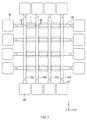
- FIG. 1 is a conceptual diagram showing a general configuration of a magnetic memory device in the embodiment.
- the magnetic memory device has an address buffer 51, a data buffer 52, a control logic part 53, a memory cell group 54, a first drive control circuit part 56, a second drive control circuit part 58, external address input terminals A0 to A20, and external data terminals D0 to D7.
- the memory cell group 54 has a matrix structure in which a number of memory cells 1 each having a pair of tunneling magneto-resistive elements (hereinbelow, called TMR elements) are arranged in a word line direction (X-direction) and a bit line direction (Y-direction) which are orthogonal to each other.
- the memory cell 1 is the minimum unit for storing data in the magnetic memory device and is a concrete example corresponding to a "magnetic memory cell" in the invention. The memory cell 1 will be described in detail later.
- the first drive control circuit part 56 has an address decoder circuit 56A, a sense amplification circuit 56B, and a current drive circuit 56C in the Y-direction.
- the second drive control circuit part 58 has an address decoder circuit 58A, a constant current circuit 58B, and a current drive circuit 58C in the X-direction.
- the address decoder circuits 56A and 58A are to select a word decode line 72 (which will be described later) and a bit decode line 71 (which will be described later) according to an input address signal.
- the sense amplification circuit 56B and the constant current circuit 58B are circuits driven at the time of performing reading operation.
- the current drive circuits 56C and 58C are circuits driven at the time of performing writing operation.
- the sense amplification circuit 56B and the memory cell group 54 are connected to each other via a plurality of bit decode lines 71 in which the sense current flows at the time of reading operation.
- the constant current circuit 58B and the memory cell group 54 are connected to each other via a plurality of word decode lines 72 in which the sense current flows at the time of reading operation.
- the address buffer 51 has the external address input terminals A0 to A20 and is connected to the Y-direction address decoder circuit 56A in the first drive control circuit part 56 via a Y-direction address line 57 and the X-direction address decoder circuit 58A in the second drive control circuit part 58 via an X-direction address line 55.
- the address buffer 51 receives an address signal from the outside via the external address input terminals A0 to A20 and amplifies the address signal to a voltage level required in the Y-direction address decoder circuit 56A and the X-direction address decoder circuit 58A by a buffer amplifier (not shown) provided in the address buffer 51.
- the data buffer 52 is constructed by an input buffer 52A and an output buffer 52B, has the external data terminals D0 to D7, is connected to the control logic part 53, and operates by an output control signal 53A from the control logic part 53.
- the input buffer 52A is connected to the Y-direction current drive circuit 56C in the first drive control circuit part 56 and the X-direction current drive circuit 58C in the second drive control circuit part 58 via a Y-direction write data bus 61 and an X-direction write data bus 60, respectively.
- the output buffer 52B functions to amplify the information signal supplied from the sense amplification circuit 56B by an internally provided buffer amplifier (not shown) and to output the resultant signal with low impedance to the external data terminals D0 to D7.
- the write word lines 6 extend in the X-direction in a rectangular wave shape and the write bit lines 5a and 5b extend in the Y-direction alternately and linearly.
- the rising and falling portions of the rectangular wave shape of the write word line 6 form the plurality of parallel parts 10a and 10b in cooperation with the write bit lines 5a and 5b.
- the memory cell 1 is provided in each region where the write bit lines 5a and 5b cross the write word line 6 so as to include at least a part of the parallel parts 10a and 10b.
- the memory cell 1 is constructed by TMR elements 1a and 1b, the TMR element 1a is provided in a region where the write bit line 5a and the write word line 6 cross each other, and the other TMR element 1b is provided in the region where the write bit line 5b and the write word line 6 cross each other.
- the TMR elements 1a and 1b are a concrete example of "a pair of magneto-resistive elements" of the invention.
- the direction of current in the write bit line 5b and that in the write word line 6 flowing in the other TMR element 1b are also parallel with each other.
- the write bit lines 5a and 5b will be simply referred to as the write bit lines 5.
- the write word line 6 is a concrete example corresponding to a "first write line” of the invention
- the write bit line 5 is a concrete example corresponding to a "second write line” of the invention.
- write bit line lead electrodes 47 are provided. One end of each of the write bit line lead electrodes 47 is connected to the Y-direction current drive circuit 56C and the other end is connected so as to be finally grounded. Similarly, write word line lead electrodes 46 are provided at both ends of each write word line 6. One end of each of the write word line lead electrodes 46 is connected to the X-direction current drive circuit 58C and the other end is connected so as to be finally grounded.
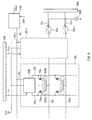
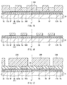
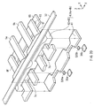
- FIG. 4 is an enlarged perspective view of the memory cell 1.
- FIG. 5 shows a schematic sectional configuration of the memory cell 1 taken along line V-V of FIG. 3.
- FIG. 6 shows the memory cell 1 of FIG. 5A which is conceptually divided into the TMR element 1a and the TMR element 1b.
- FIGs. 5 and 6 are schematic diagrams for clarifying the configuration of detailed parts. The size ratio and shape of the memory cell 1 shown in FIGs. 5 and 6 do not always coincide with those shown in FIG. 4.
- the memory cell 1 has the pair of TMR elements 1a and 1b including the magnetic yokes 4a and 4b and the stacked bodies S20a and S20b, respectively.
- the write bit lines 5a and 5b and write word line 6 (part of the first level 6F) are disposed so as to be adjacent to each other in the first level L1 parallel with the stacked layer surface of the stacked bodies S20a and S20b in the region surrounded by the magnetic yokes 4a and 4b (FIG. 5).
- the write word line 6 (part of the first level 6F), write bit lines 5a and 5b, and magnetic yokes 4a and 4b are electrically insulated from each other via insulating films 7a and 7b.
- the stacked bodies S20a and S20b are formed on the surface parallel with the direction of arranging the write word line 6 (part of the first level 6F) and the write bit lines 5a and 5b, in the outer surface of the magnetic yokes 4a and 4b.
- the stacked bodies S20a and S20b are electrically connected to conductive layers 36a and 36b (which will be described later) formed on the side opposite to the magnetic yokes 4a and 4b in the Z-direction.
- the stacked bodies S20a and S20b are TMR films including, in order from the side of the magnetic yokes 4a and 4b, the second magnetic layers 8a and 8b, tunnel barrier layers 3a and 3b, and first magnetic layers 2a and 2b whose magnetization direction is fixed, and are constructed so that current flows in the direction perpendicular to the stacked face.
- the stacked bodies S20a and S20b are exaggerated so as to be larger relative to the peripheral parts.
- the second magnetic layers 8a and 8b as magneto-sensitive layers (also called free magnetization direction layers) are magnetically exchange-coupled with connection parts 14a and 14b as part of the magnetic yokes 4a and 4b.
- MR ratio magneto-resistance change ratio
- tunnel resistance Rt The resistance value against the tunnel current (hereinbelow, called tunnel resistance Rt) strongly depends on the thickness T of the tunnel barrier layer 3.
- the tunnel resistance Rt exponentially increases with the thickness T of the tunnel barrier layer 3.
- Rt ⁇ exp(2 ⁇ T ), ⁇ ⁇ 8 ⁇ 2 m*( ⁇ Ef) 0.5 ⁇ /h
- ⁇ denotes the height of the barrier
- m* denotes effective mass of electrons
- Ef indicates Fermi energy
- h indicates a Planck's constant.
- the proper tunnel resistance Rt is about tens k ⁇ ⁇ ( ⁇ m) 2 .
- the tunnel resistance Rt is set to, preferably, 10 kQ ⁇ ( ⁇ m) 2 or less, more preferably, 1k ⁇ ( ⁇ m) 2 or less. Therefore, to realize the tunnel resistance Rt, it is desirable to set the thickness T of the tunnel barrier layer 3 to 2 nm or less, more preferably, 1.5 nm or less.
- the stacked bodies S20a and S20b have a coercive force differential structure and the coercive force of the first magnetic layers 2a and 2b is larger than that of the second magnetic layers 8a and 8b.
- the coercive force of the first magnetic layer 2 is preferably larger than (50/4 ⁇ ) ⁇ 10 3 A/m, more preferably, (100/4 ⁇ ) ⁇ 10 3 A/m.
- the first magnetic layers 2a and 2b are made of, for example, cobalt iron alloy (CoFe) and have a thickness of 5 nm.
- cobalt (Co), cobalt platinum alloy (CoPt), nickel iron cobalt alloy (NiFeCo), or the like can be applied to the first magnetic layers 2a and 2b.
- the second magnetic layers 8a and 8b are made of, for example, cobalt (Co), cobalt iron alloy (CoFe), cobalt platinum alloy (CoPt), nickel iron alloy (NiFe), or nickel iron cobalt alloy (NiFeCo).
- the axes of easy magnetization of the first magnetic layers 2a and 2b and the second magnetic layers 8a and 8b are preferably parallel with each other since the magnetization direction of the first magnetic layers 2a and 2b and that of the second magnetic layers 8a and 8b are stabilized in a parallel or antiparallel state.
- the magnetic yokes 4a and 4b extend so as to annularly surround at least a part of the parallel parts 10a and 10b in the write bit lines 5a and 5b and the write word line 6 and are constructed so that a return magnetic field is generated in the magnetic yokes 4a and 4b by current flowing in the parallel parts 10a and 10b. More specifically, as shown in FIG.
- the magnetic yoke 4a includes: a pair of pillar yokes 42a (421 and 422) extending in the direction (Z-direction) orthogonal to the stacked layer face of the stacked body S20a while facing each other over the write bit line 5a and the part of the first level 6F; a first beam yoke 41a connected to one end on the side of the stacked body S20a of each of the pair of pillar yokes 42a (421 and 422); and a second beam yoke 43a connected to the other end of each of the pair of pillar yokes 42a (421 and 422).
- the magnetic yoke 4a has a closed sectional shape.
- the other magnetic yoke 4b includes: a pair of pillar yokes 42b (422 and 423) extending in the direction (Z-direction) orthogonal to the stacked layer face of the stacked body S20b while facing each other over the write bit line 5b and the part of the first level 6F; a first beam yoke 41b connected to one end on the side of the stacked body S20b of each of the pair of pillar yokes 42b (422 and 423); and a second beam yoke 43b connected to the other end of each of the pair of pillar yokes 42b (422 and 423).
- the magnetic yoke 4b also has a closed sectional shape.
- the first beam yoke 41a has an inherent region 411 and a common region 412
- the other first beam yoke 41b has an inherent region 413 and a common region 412.
- the pair of pillar yokes 42a has the inherent pillar yoke 421 and the common pillar yoke 422.
- the other pair of pillar yokes 42b has the inherent pillar yoke 423 and the common pillar yoke 422.
- the second beam yoke 43a has an inherent region 431 and a common region 432.
- the other second beam yoke 43b has an inherent region 433 and the common region 432.
- the TMR elements 1a and 1b share the common region 412 of the first beam yokes 41a and 41b, the pillar yoke 422 shared by the pillar yokes 42a and 42b, and the common region 432 of the second beam yokes 43a and 43b, and the common part 34 is formed as shown in FIG. 5.
- the second beam yokes 43a and 43b are provided in the second level L2 at which the part of the second level 6S is also provided.
- the magnetization direction of the second magnetic layers 8a and 8b is not influenced and is stably held.
- the coercive force of the connection parts 14a and 14b in the magnetic yokes 4a and 4b is smaller than that of the first magnetic layers 2a and 2b within the range of (100/4 ⁇ ) ⁇ 10 3 A/m or less for the following reason.
- the coercive force exceeds (100/4 ⁇ ) ⁇ 10 3 A/m, there is the possibility that the stacked bodies S20a and S20b themselves as the TMR films deteriorate due to heat generation caused by increase in write current.
- the magnetic permeability of the magnetic yokes 4a and 4b is preferably high. Concretely, the magnetic permeability is preferably 2000 or higher and, more preferably, 6000 or higher.
- Each of the write bit lines 5a and 5b and the part of the first level 6F has a structure in which, for example, a film of titanium (Ti) having a thickness of 10 nm, a film of titanium nitride (TiN) having a thickness of 10 nm, and a film of aluminum (Al) having a thickness of 500 nm are sequentially stacked.
- the part of the second level 6S and the connection layer 6T are made of the same kind of material, for example, NiFe as that of the magnetic yokes 4a and 4b.
- the write bit line 5 and the write word line 6 are not limited to have the above configuration but may be made of at least one of aluminum (Al), copper (Cu), and tungsten (W). The details of operation of writing information to the memory cell 1 by using the write bit line 5 and the write word line 6 will be described later.
- the magnetic memory device of the embodiment has a simpler configuration in the layer stack direction since the write bit lines 5a and 5b and the write word line 6 are disposed so as to be adjacent to each other at the first level L1 parallel with the layer stack face of the stacked bodies S20a and S20b in the region surrounded by the magnetic yokes 4a and 4b.
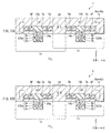
- FIG. 7 is a plan view showing the configuration of a main part related to the reading operation of the memory cell group 54 and corresponds to FIG. 3.
- FIG. 8 is a cross section taken along line VIII-VIII of FIG. 7.
- the magnetic memory device of the embodiment is constructed so that, in a region including the memory cell 1, the pair of stacked bodies S20a and S20b and the magnetic yokes 4a and 4b are sequentially formed over the substrate 31 provided with the Schottky diode 75 (hereinbelow, simply called diode 75) functioning as a rectifier.
- the Schottky diode 75 hereinbelow, simply called diode 75
- the substrate 38 is an n - type silicon wafer. Generally, in the n - type silicon wafer, an impurity of phosphorus (P) is diffused. As the substrate 38, a wafer of an n ++ type obtained by being highly doped with phosphorus is used. In contrast, as the epitaxial layer 37, a wafer of the n - type obtained by being lightly doped with phosphorus is used. By making the epitaxial layer 37 as an n - type semiconductor and the conductive layers 36a and 36b made of a metal come into contact with each other, a band gap is created and a Schottky barrier is formed. Further, the pair of diodes 75a and 75b are connected to the read bit lines 33a and 33b, respectively, via a connection layer 33T.
- FIG. 9 the circuit configuration related to the reading operation in the magnetic memory device of the embodiment will be described.
- FIG. 9 is a configuration diagram of a circuit system constructed by the memory cell group 54 and a read circuit.
- the memory cell 1 is of a differential amplifier type constructed by the pair of TMR elements 1a and 1b.
- Information in the memory cell 1 is read by outputting a differential value of read currents passed to the TMR elements 1a and 1b (currents passed from the read bit lines 33a and 33b to the TMR elements 1a and 1b and output to the common read word line 32).
- the read word lines 32 (..., 32m, 32m+1, ...) arranged in the X-direction and the pair of read bit lines 33a and 33b arranged in the Y-direction are disposed in a matrix.
- Each of the memory cells 1 is disposed in a position intersecting with the read word line 32 in a region sandwiched by the pair of read bit lines 33a and 33b.
- One end of each of the TMR elements 1a and 1b in each memory cell 1 is connected to the read bit lines 33a and 33b via the pair of diodes 75a and 75b, respectively, and the other ends are connected to the common read word line 32.
- each read word line 32 is connected to a read switch 83 (..., 83 m , 83 m+1 , ...) via the read word line lead electrode 48 and is also connected to a common constant current circuit 58B.
- Each read switch 83 is connected to the X-direction address decoder circuit 58A via the word decode line 72 (..., 72 m , 72 m+1 , ).
- the read switch 83 is made conductive when a selection signal from the X-direction address decoder circuit 58A is supplied.
- the constant current circuit 58B has the function of making the current flowing in the read word line 32 constant.
- each read bit line 33 is connected to the sense amplification circuit 56B via the read bit line lead electrode 49, and the other end is finally grounded.
- One sense amplification circuit 56B is provided per unit read circuit 80 and has the function of receiving the potential difference between the pair of read bit lines 33a and 33b in each unit read circuit 80 and amplifying the potential difference.
- Each of the sense amplification circuits 56B is connected to the output line 82 (..., 82n, 82n+1, ...) and is finally connected to the output buffer 52B via the Y-direction read data bus 62.
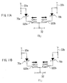
- FIGs. 10A and 10B express the relation between the write current direction and the return magnetic field direction (magnetization direction) in the sectional configuration of the memory cell 1 shown in FIG. 5.
- the arrows indicated in magnetic layers in FIGs. 10A and 10B indicate the magnetization directions of the magnetic layers.
- the magnetic yokes 4a and 4b the magnetic field directions of a magnetic path formed on the inside are also shown.
- the magnetization of the first magnetic layers 2a and 2b is fixed to the ⁇ X direction.
- FIG. 10A and 10B show the case where write current flows in the same direction to the write bit line 5 and the write word line 6 which extend in the memory cell 1 and are parallel with each other.
- FIG. 10A corresponds to the write current direction shown in FIG. 2.
- FIG. 10A shows a case where write current flows from this side to the depth in the direction perpendicular to the drawing sheet (in the +Y direction) in the TMR element 1a and a return magnetic field 16a is generated in the clockwise direction in the magnetic yoke 4a of the portion surrounding the write bit line 5a and the part of the first level 6F, and also a case where write current flows from the depth to this side in the direction perpendicular to the drawing sheet (in the -Y direction) in the TMR element 1b, and the return magnetic field 16b is generated in the counterclockwise direction in the magnetic yoke 4b of the portion surrounding the write bit line 5b and the part of the first level 6F.
- FIG. 10B corresponds to the case where the directions of current flowing in the write bit line 5 and the part of the first level 6F are opposite to those shown in FIG. 10A. Specifically, FIG.
- the magnetization direction of the connection part 14a and the second magnetic layer 8a and that of the connection part 14b and the second magnetic layer 8b change so as to be opposite to each other.
- information can be stored in the memory cell 1.
- the second magnetic layers 8a and 8b are provided between the tunnel barrier layers 3a and 3b and the connection parts 14a and 14b of the magnetic yokes 4a and 4b, the following advantages are obtained.
- Exchange coupling between the connection parts 14a and 14b and the second magnetic layers 8a and 8b can be realized and the magnetization direction in the second magnetic layers 8a and 8b is aligned more excellently, so that more stable writing can be performed.
- the coercive force of the connection parts 14a and 14b can be further suppressed, so that a heat generation amount can be decreased by reducing the current value in the writing operation, and the functions of the magnetic memory device can be fully displayed.
- the magnetic memory device of the embodiment as described above, by passing current to both of the write bit lines 5a and 5b and the write word line 6, a closed magnetic circuit can be formed. Consequently, magnetization in the magnetic yokes 4a and 4b in the TMR elements 1a and 1b can be inverted efficiently, and the magnetic influences on memory cells adjacent to the memory cell 1 to be subject to writing can be reduced. Further, by the shield effect of the magnetic yokes 4a and 4b, the intervals of neighboring memory cells on the substrate can be narrowed. Thus, the invention has the advantage of realizing higher integration and higher packing density of the magnetic memory device.
- FIGs. 11A and 11B are circuit diagrams each showing a portion around the memory cell 1.
- the magnetization directions of the first magnetic layers 2a and 2b in the stacked bodies S20a and S20b are indicated by hollow arrows and those of the second magnetic layers 8a and 8b are indicated by solid arrows. Both of the magnetization directions of the first magnetic layers 2a and 2b are fixed to the left directions.
- the magnetization direction of the first magnetic layer 2a and that in the second magnetic layer 8a in the stacked body S20a are the same, and the magnetization direction of the first magnetic layer 2b and that of the second magnetic layer 8b in the other stacked body S20b are opposite to each other.
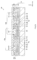
- FIGs. 12 to 19 are cross sections taken along line ⁇ - ⁇ '- ⁇ shown in FIG. 3 and show manufacturing processes in order.
- the lower yoke 4B (the first beam yokes 41a and 41b) is formed over the substrate 31 via the stacked bodies S20a and S20b.
- the substrate 31 in which the diodes 75a and 75b are buried and on which the stacked bodies S20a and S20b and the insulating film 17A surrounding the stacked bodies S20a and S20b and its periphery are already formed is prepared.
- the details of the substrate 31 will be omitted.
- a metal film made of NiFe is formed by, for example, sputtering on the entire surface. After that, the metal film is subjected to milling so as to leave the region corresponding to the stacked bodies S20a and S20b, thereby obtaining the lower yoke 4B.
- the upper magnetic yoke 4U (specifically, the pair of pillar yokes 42 and the second beam yoke 43) and the part of the second level 6S are formed.
- an insulating film 7B made of, for example, Al 2 O 3 is formed so as to cover the entire face by sputtering or the like and, after that, a resist pattern 30B is selectively formed on the insulating film 7B.
- the resist pattern 30B is formed so as not to cover both sides of the regions in which the write bit lines 5a and 5b and the part of the first level 6F are formed in the region in which the lower yoke 4B is formed, and a partial region corresponding to the part of the first level 6F in the region in which the lower yoke 4B is not formed.
- the resist pattern 30B is used as a mask, and the insulating films 7A and 7B in non-protect regions are removed by reactive ion etching (RIE) or the like.
- RIE reactive ion etching
- the write word line lead electrodes 46 are formed at both ends of the write word line 6
- the write bit line lead electrodes 47 are formed at both ends of the write bit line 5
- the read word line lead electrodes 48 are formed at both ends of the read word line 32 and, further, the read bit line lead electrodes 49 are formed at both ends of the read bit line 33.
- the method of manufacturing a magnetic memory device of the embodiment includes the step of simultaneously forming the write bit lines 5a and 5b and the part of the first level 6F. Consequently, as compared with the case where the write bit lines 5a and 5b and the part of the first level 6F are formed separately, the memory cell 1 can be formed by the smaller number of processes.
- the magnetic yoke forming step includes a step of simultaneously forming the part of the second level 6S and the upper magnetic yoke 4U in a region other than the region surrounded by the magnetic yokes 4a and 4b, so that the manufacturing process can be further simplified.
- the part of the second level 6S as a connection conductor is provided in the same level as the beam yoke on the furthest side from the stacked bodies S20a and S20b.
- the invention is not limited to the configuration.
- the part of the second level 6S may be provided at the same level as that of a pair of beam yokes 41a and 41b on the side close to the stacked bodies S20a and S20b.
- the memory cell 120 has: a TMR element 120a including the magnetic yoke 4a constructed by a pair of pillar yokes 421 and 422 facing each other and extending in the direction orthogonal to the layer stacked face of the stacked body S20a and a beam yoke 141a connected to one end on the side of the stacked body S20a of each of the pair of pillar yokes 421 and 422; and a TMR element 120b including the magnetic yoke 4b constructed by a pair of pillar yokes 422 and 423 facing each other and extending in the direction orthogonal to the layer stacked face of the stacked body S20b and a beam yoke 141b connected to one end on the side of the stacked body S20b of each of the pair of pillar yokes 422 and 423.
- the pair of TMR elements 120a and 120b share the pillar yoke 422 and the common region 412 of the beam yokes 141a and 141b.
- the write bit lines 5a and 5b and the part of the first level 6F are arranged so as to be adjacent to each other in the first level L1 including the plane parallel with the layer stacked face of the stacked bodies S20a and S20b in the region surrounded by the magnetic yokes 4a and 4b. Therefore, at the time of manufacture, the write bit lines 5a and 5b and the part of the first level 6F can be simultaneously formed in the region surrounded by the magnetic yokes 4a and 4b, and the number of processes can be reduced.
- the number of processes can be further decreased. It is not always necessary to provide the pillar yokes 421 to 423. That is, a memory cell having the shape obtained by removing the pillar yokes 421 to 423 in the memory cell 122 shown in FIG. 21 may be also realized.
- the stacked body is not limited to the configuration that current flows in the direction orthogonal to the layer stacked face but may be constructed so that current flows along the layer stacked face.
- connection parts 84a and 84b as part of the magnetic yokes 4a and 4b can also serve as the magneto-sensitive layers in the stacked bodies S22a and S22b.
- the connection parts 84a and 84b as part of the magnetic yokes 4a and 4b also function as the magneto-sensitive layers in the stacked bodies S22a and S22b. Consequently, the second magnetic layers 8a and 8b provided in the TMR elements 1a and 1b can be omitted, and the memory cell 122 having a configuration simpler than that of the memory cell 1 can be achieved.
- the magnetic memory cell having a pair of magneto-resistive elements has been described in the foregoing embodiment, the invention is not limited to the magnetic memory cell.
- a single TMR element having one magnetic yoke 4 and one stacked body S20 may be used as a magnetic memory element.
- the memory cell constructed by the single TMR element like a TMR element 124 (sixth modification) shown in FIG. 25, not the magnetic yoke constructed so as to surround the whole periphery of the first and second write lines but a magnetic yoke having a U shape in cross section, a part of which is open may be provided.
Landscapes
- Engineering & Computer Science (AREA)
- Computer Hardware Design (AREA)
- Mram Or Spin Memory Techniques (AREA)
- Hall/Mr Elements (AREA)
- Semiconductor Memories (AREA)
Applications Claiming Priority (2)
| Application Number | Priority Date | Filing Date | Title |
|---|---|---|---|
| JP2003342623 | 2003-09-30 | ||
| JP2003342623A JP2005109266A (ja) | 2003-09-30 | 2003-09-30 | 磁気メモリデバイスおよび磁気メモリデバイスの製造方法 |
Publications (2)
| Publication Number | Publication Date |
|---|---|
| EP1524672A2 true EP1524672A2 (fr) | 2005-04-20 |
| EP1524672A3 EP1524672A3 (fr) | 2007-05-16 |
Family
ID=34373505
Family Applications (1)
| Application Number | Title | Priority Date | Filing Date |
|---|---|---|---|
| EP04023232A Withdrawn EP1524672A3 (fr) | 2003-09-30 | 2004-09-29 | Dispositif de mémoire magnetique et un procédé de fabrication d'un dispositif de mémoire magnetique |
Country Status (4)
| Country | Link |
|---|---|
| US (1) | US7157760B2 (fr) |
| EP (1) | EP1524672A3 (fr) |
| JP (1) | JP2005109266A (fr) |
| CN (1) | CN1604229A (fr) |
Cited By (1)
| Publication number | Priority date | Publication date | Assignee | Title |
|---|---|---|---|---|
| TWI804225B (zh) * | 2021-03-16 | 2023-06-01 | 日商鎧俠股份有限公司 | 磁性記憶裝置及磁性記憶裝置之製造方法 |
Families Citing this family (4)
| Publication number | Priority date | Publication date | Assignee | Title |
|---|---|---|---|---|
| JP2005109266A (ja) * | 2003-09-30 | 2005-04-21 | Tdk Corp | 磁気メモリデバイスおよび磁気メモリデバイスの製造方法 |
| JP4779608B2 (ja) * | 2005-11-30 | 2011-09-28 | Tdk株式会社 | 磁気メモリ |
| KR100790886B1 (ko) * | 2006-09-15 | 2008-01-03 | 삼성전자주식회사 | 자구 벽 이동을 이용한 정보 저장 장치 |
| DE102022108102A1 (de) * | 2022-04-05 | 2023-10-05 | Infineon Technologies Ag | Magnetische sensorvorrichtung |
Family Cites Families (10)
| Publication number | Priority date | Publication date | Assignee | Title |
|---|---|---|---|---|
| US5343422A (en) * | 1993-02-23 | 1994-08-30 | International Business Machines Corporation | Nonvolatile magnetoresistive storage device using spin valve effect |
| US5629922A (en) * | 1995-02-22 | 1997-05-13 | Massachusetts Institute Of Technology | Electron tunneling device using ferromagnetic thin films |
| JP3333670B2 (ja) | 1995-09-22 | 2002-10-15 | ティーディーケイ株式会社 | 磁性薄膜メモリ |
| DE19836567C2 (de) * | 1998-08-12 | 2000-12-07 | Siemens Ag | Speicherzellenanordnung mit Speicherelementen mit magnetoresistivem Effekt und Verfahren zu deren Herstellung |
| JP2001273759A (ja) | 2000-03-27 | 2001-10-05 | Sharp Corp | 磁気メモリセルと磁気メモリ装置 |
| US7068530B2 (en) * | 2002-12-27 | 2006-06-27 | Tdk Corporation | Magnetoresistive effect element and memory device using the same |
| JP2005044847A (ja) * | 2003-07-23 | 2005-02-17 | Tdk Corp | 磁気抵抗効果素子、磁気記憶セルおよび磁気メモリデバイスならびにそれらの製造方法 |
| JP2005109266A (ja) * | 2003-09-30 | 2005-04-21 | Tdk Corp | 磁気メモリデバイスおよび磁気メモリデバイスの製造方法 |
| JP4868431B2 (ja) * | 2003-10-10 | 2012-02-01 | Tdk株式会社 | 磁気記憶セルおよび磁気メモリデバイス |
| JP4438375B2 (ja) * | 2003-10-21 | 2010-03-24 | Tdk株式会社 | 磁気抵抗効果素子、磁気記憶セルおよび磁気メモリデバイス |
-
2003
- 2003-09-30 JP JP2003342623A patent/JP2005109266A/ja not_active Withdrawn
-
2004
- 2004-09-28 US US10/950,399 patent/US7157760B2/en not_active Expired - Fee Related
- 2004-09-29 EP EP04023232A patent/EP1524672A3/fr not_active Withdrawn
- 2004-09-30 CN CNA2004100851912A patent/CN1604229A/zh active Pending
Cited By (1)
| Publication number | Priority date | Publication date | Assignee | Title |
|---|---|---|---|---|
| TWI804225B (zh) * | 2021-03-16 | 2023-06-01 | 日商鎧俠股份有限公司 | 磁性記憶裝置及磁性記憶裝置之製造方法 |
Also Published As
| Publication number | Publication date |
|---|---|
| JP2005109266A (ja) | 2005-04-21 |
| CN1604229A (zh) | 2005-04-06 |
| US7157760B2 (en) | 2007-01-02 |
| US20050068825A1 (en) | 2005-03-31 |
| EP1524672A3 (fr) | 2007-05-16 |
Similar Documents
| Publication | Publication Date | Title |
|---|---|---|
| US6839269B2 (en) | Magnetic random access memory | |
| EP1511041B1 (fr) | Cellule mémoire magnétique, dispositif mémoire magnétique et méthode pour les produire | |
| JPWO2009110532A1 (ja) | 半導体装置 | |
| EP1528569B1 (fr) | Elément magnétorésistif,cellule de mémoire magnétique et dispositif de mémoire magnétique | |
| JP4729836B2 (ja) | 磁気記憶セルおよび磁気メモリデバイスならびに磁気メモリデバイスの製造方法 | |
| EP1523011B1 (fr) | Elément magnétorésistif, cellule de mémoire magnétique et dispositif de mémoire magnétique | |
| EP1524672A2 (fr) | Dispositif de mémoire magnetique et un procédé de fabrication d'un dispositif de mémoire magnetique | |
| JP4720067B2 (ja) | 磁気記憶セルおよび磁気メモリデバイスならびに磁気メモリデバイスの製造方法 | |
| EP1679719B1 (fr) | Elément magnétorésistif, cellule de mémoire magnétique, et dispositif de mémoire magnétique | |
| JP4556385B2 (ja) | 磁気メモリデバイスの製造方法 |
Legal Events
| Date | Code | Title | Description |
|---|---|---|---|
| PUAI | Public reference made under article 153(3) epc to a published international application that has entered the european phase |
Free format text: ORIGINAL CODE: 0009012 |
|
| AK | Designated contracting states |
Kind code of ref document: A2 Designated state(s): AT BE BG CH CY CZ DE DK EE ES FI FR GB GR HU IE IT LI LU MC NL PL PT RO SE SI SK TR |
|
| AX | Request for extension of the european patent |
Extension state: AL HR LT LV MK |
|
| PUAL | Search report despatched |
Free format text: ORIGINAL CODE: 0009013 |
|
| AK | Designated contracting states |
Kind code of ref document: A3 Designated state(s): AT BE BG CH CY CZ DE DK EE ES FI FR GB GR HU IE IT LI LU MC NL PL PT RO SE SI SK TR |
|
| AX | Request for extension of the european patent |
Extension state: AL HR LT LV MK |
|
| AKX | Designation fees paid | ||
| STAA | Information on the status of an ep patent application or granted ep patent |
Free format text: STATUS: THE APPLICATION IS DEEMED TO BE WITHDRAWN |
|
| 18D | Application deemed to be withdrawn |
Effective date: 20071117 |
|
| REG | Reference to a national code |
Ref country code: DE Ref legal event code: 8566 |