EP1524572A2 - Spannungsversorgungsanordnung und Verfahren - Google Patents
Spannungsversorgungsanordnung und Verfahren Download PDFInfo
- Publication number
- EP1524572A2 EP1524572A2 EP04023256A EP04023256A EP1524572A2 EP 1524572 A2 EP1524572 A2 EP 1524572A2 EP 04023256 A EP04023256 A EP 04023256A EP 04023256 A EP04023256 A EP 04023256A EP 1524572 A2 EP1524572 A2 EP 1524572A2
- Authority
- EP
- European Patent Office
- Prior art keywords
- output
- power
- switch
- current
- regulator
- Prior art date
- Legal status (The legal status is an assumption and is not a legal conclusion. Google has not performed a legal analysis and makes no representation as to the accuracy of the status listed.)
- Granted
Links
Images


Classifications
-
- H—ELECTRICITY
- H02—GENERATION; CONVERSION OR DISTRIBUTION OF ELECTRIC POWER
- H02M—APPARATUS FOR CONVERSION BETWEEN AC AND AC, BETWEEN AC AND DC, OR BETWEEN DC AND DC, AND FOR USE WITH MAINS OR SIMILAR POWER SUPPLY SYSTEMS; CONVERSION OF DC OR AC INPUT POWER INTO SURGE OUTPUT POWER; CONTROL OR REGULATION THEREOF
- H02M3/00—Conversion of dc power input into dc power output
- H02M3/02—Conversion of dc power input into dc power output without intermediate conversion into ac
- H02M3/04—Conversion of dc power input into dc power output without intermediate conversion into ac by static converters
- H02M3/10—Conversion of dc power input into dc power output without intermediate conversion into ac by static converters using discharge tubes with control electrode or semiconductor devices with control electrode
- H02M3/145—Conversion of dc power input into dc power output without intermediate conversion into ac by static converters using discharge tubes with control electrode or semiconductor devices with control electrode using devices of a triode or transistor type requiring continuous application of a control signal
- H02M3/155—Conversion of dc power input into dc power output without intermediate conversion into ac by static converters using discharge tubes with control electrode or semiconductor devices with control electrode using devices of a triode or transistor type requiring continuous application of a control signal using semiconductor devices only
- H02M3/156—Conversion of dc power input into dc power output without intermediate conversion into ac by static converters using discharge tubes with control electrode or semiconductor devices with control electrode using devices of a triode or transistor type requiring continuous application of a control signal using semiconductor devices only with automatic control of output voltage or current, e.g. switching regulators
- H02M3/157—Conversion of dc power input into dc power output without intermediate conversion into ac by static converters using discharge tubes with control electrode or semiconductor devices with control electrode using devices of a triode or transistor type requiring continuous application of a control signal using semiconductor devices only with automatic control of output voltage or current, e.g. switching regulators with digital control
Definitions
- This invention relates to output regulators.
- Output regulators are employed in numerous machines and devices including Virtually every electronic device.
- An output regulator typically converts unregulated input power to one or more regulated outputs for supplying power to circuits within the machine or device.
- the regulated outputs are most commonly regulated voltage, but regulated current and regulated power may also be generated.
- the output regulator may be integrated into the machine or device, or the output regulator may be a separate assembly that is assembled to machine or device.
- Several characteristics of output regulators may be used to judge the quality of a particular design including operating characteristics such as power density, efficiency, output regulation, and transient response. Improvements in the operating characteristics of output regulators are desirable so that machines and devices that use output regulators may be improved such as by being made smaller, requiring less power, having improved accuracy and reliability, or having improved operation during transient conditions.
- a control system and method for controlling an output regulator having a regulated output In one aspect, a control system and method for controlling an output regulator having a regulated output.
- An output sensor to generate a digital sense signal to indicate within which of at least three reference ranges the regulated output is included. Each of the at least three reference ranges including a plurality of possible values of the regulated output.
- a digital controller responsive to the digital sense signal, to generate a drive signal to control the regulated output.
- an output regulator and method to convert an input voltage to a regulated output The output regulator including a power stage to generate a power output from the input voltage. An output filter to filter the power output to generate the regulated output. An output sensor to generate a digital sense signal to indicate within which of at least three reference ranges the regulated output is included. Each of the at least three reference ranges including a plurality of possible values of the regulated output. A digital controller, responsive to the digital sense signal, to generate a drive signal to control the power stage.
- a circuit and method for generating a feedback signal corresponding to a first voltage comprising a reference generator to generate at least two reference voltages.
- the reference voltages to define at least three voltage ranges.
- a comparator to compare the first voltage to the at least three voltage ranges and to generate a digital signal to indicate within which of the at least three reference ranges the regulated output is included.
- a power array and method for converting an input voltage to a chopped output An output regulator to convert the chopped output to a regulated output
- the power array comprising a switch array, responsive to independent drive signals, to convert the input voltage to the chopped output at a switching frequency.
- the switch array including at least two power switches.
- a switch controller to generate the independent drive signals as a function of a duty cycle signal.
- the switch controller to operate at a sampling frequency, the sampling frequency being greater than the switching frequency.
- the switch controller to control the independent drive signals at a drive frequency greater than the switching frequency.
- a method and system of sensing current in an output regulator comprising providing a current sensor having a gain resolution, setting the current sensor gain resolution to an initial resolution, sensing a current flowing through the current sensor, evaluating an amplitude of the current, and at a sampling frequency, controlling the gain resolution of the current sensor based on the evaluating.
- a method and system of controlling deadtime between power switches in an output regulator comprising providing at least two power switches having a common node, wherein at least one of the two power switches is a conducting switch and a remainder of the two power switches is a free-wheeling switch. Switching one of the conducting switch and the free-wheeling switch from an on-state to an off-state. During a transition from the on-state to the off-state, monitoring a current flowing through one of the conducting switch and the free-wheeling switch. Comparing the current to a reference level. Delaying for a predetermined time period, then changing the operating state of the other of the conducting switch and the freewheeling switch from an off-state to an on-state.
- a method and system of reducing switching losses in a switch array for an output regulator comprising determining an expected current flowing through the switch array during a next switching cycle. At a sampling rate, determining expected power losses of the switch array based on the expected current. Determining a combination of the power switches to enable that minimizes the expected power losses. Enabling the combination of power switches.
- a method and system of suppressing noise in a power stage for an output regulator comprising monitoring a noise characteristic of the common node, comparing the noise characteristic to a reference level, generating an impedance control signal based on the comparing, and at a sampling rate controlling the switch arrays in response to the impedance control signal.
- a method and system of controlling a capacitance of a circuit node of a power stage for an output regulator comprising monitoring a current flowing through the switch array, determining a desired capacitance at the circuit node based on the current, at a sampling rate determining a combination of switch assemblies to enable to set the circuit node to the desired capacitance, and controlling the series pairs of power switches to set the circuit node to the desired capacitance.
- a diode emulation system and method to convert energy from an input source to a regulated output of an output regulator comprising a first power switch, responsive to a first drive signal, to control a flow of energy from the input source to an output inductor of the output regulator such that a current flowing through the output inductor increases.
- a switch array including at least two power switches, responsive to array drive signals, to provide a path for the current flowing through output inductor during a freewheeling phase such that current flowing through the output inductor decreases.
- a current sensor to sense a current flowing through the switch array, and a controller to generate the array drive signals as a function of the current flowing through the switch array. The controller to independently control the at least two power switches.
- a duty cycle limiter and method for limiting a transfer of energy between an input source and a regulated output of an output regulator having a regulator characteristic and a computed duty cycle for controlling the transfer of energy between the input source and the regulated output.
- the duty cycle limiter comprising a digital controller to generate a reference level and to compare the regulator characteristic of the output regulator to the reference level to determine a maximum duty cycle.
- the digital controller to control the reference level at a frequency at least equal to a switching frequency of the output regulator.
- the digital controller to limit the computed duty cycle to the maximum duty cycle.
- a duty cycle estimator and method for determining a nominal duty cycle of an output regulator comprising at least two modes including a mode one estimator and a mode two estimator.
- the mode one estimator to determine the nominal duty cycle as a function of prior duty cycles.
- the mode two estimator to determine the nominal duty cycle as a function of accumulated error.
- a mode selector to, based on a mode selection criteria, select a one of the at least two modes to generate the nominal duty cycle.
- a digital controller and method for controlling a regulated output of an output regulator responsive to a pulse width signal for controlling the transfer of energy between an input source and the regulated output
- the digital controller comprising a duty cycle estimator to determine a nominal duty cycle.
- An adjust determiner to determine an adjustment value to combine with the nominal duty cycle to generate an adjusted duty cycle, the pulse width signal being a function of the adjusted duty cycle.
- a duty cycle estimator and method for determining a duty cycle for controlling a regulated output of an output regulator responsive to the duty cycle for controlling the transfer of energy between an input source and the regulated output.
- the duty cycle estimator comprising an accumulator to determine an accumulated error over a time period greater than a switching period of the output regulator.
- a reference generator to generate reference levels.
- a comparator to compare the accumulated error to the reference levels at a maximum rate greater than the switching period such that a single zero is generated, and to generate the duty cycle based on the comparing.
- a digital controller and method for controlling an output regulator having sub-blocks for providing functions to control the output regulator.
- the digital controller comprising an energy saving discontinuous mode (ESDM) controller to monitor a sense point of the output regulator. The sense point to indicate an output power state of the output regulator.
- the ESDM controller to control a flow of power to the sub-blocks to reduce power consumption of the digital controller during selected power states of the output regulator.
- ESDM energy saving discontinuous mode
- FIG. 1 is a block diagram of an aspect of an output regulator.
- FIG. 2 is a block diagram of an aspect of a digital controller for an output regulator.
- FIG. 5 is a state diagram of an aspect of an adaptive multi-mode control system.
- FIG. 6 is a graph of an output voltage during tum-on.
- FIG. 7 is a flow diagram of an aspect of the operation of an adaptive multi-mode control system.
- FIG. 8 is a block diagram of an aspect of an output regulator having an output slicer.
- FIG. 11 is a flow diagram of an aspect of the operation of an output slicer.
- FIG. 12A is a block diagram of an aspect of a power array.
- FIG. 13 is a timing diagram of waveforms associated with an aspect of sensing current in a power array.
- FIG. 15 is a flow diagram of an aspect of the operation of a current sensing technique.
- FIG. 17 is a timing diagram of waveforms associated with an aspect of a diode emulation system.
- FIG. 18 is a flow diagram of an aspect of the operation of a diode emulation system.
- FIG. 19 is a flow diagram of an aspect of the operation of a deadtime control technique implemented with a diode emulation system.
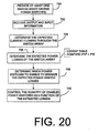
- FIG. 20 is a flow diagram of an aspect of an operation for controlling losses in a power array.
- FIG. 21 is a flow diagram of an aspect of an operation for suppressing the generation of noise by a power stage of a power regulator.
- FIG. 22 is a flow diagram of an aspect of an operation for controlling a capacitance of a circuit node of an output regulator.
- FIG. 23 is a block diagram of an aspect of a delay line for generating a delay in a pulse signal.
- FIG. 24 is a timing diagram of waveforms associated with an aspect of a delay line.
- FIG. 25 is a flow diagram of an aspect of an operation for increasing the resolution of a pulse width signal for an output regulator.
- FIG. 26 is a block diagram of an aspect of a digital controller for determining a duty cycle for a switching regulator.
- FIG. 27 is a block diagram of an aspect of a digital controller for a switching regulator.
- FIG. 28 is a state diagram of an aspect of a duty cycle estimator.
- FIG. 29 is a graphical diagram of voltage levels associated with an aspect of voltage slicer.
- FIG. 30 is a timing diagram of waveforms associated with an aspect of digital controller for generating a duty cycle for a switching regulator.
- FIG. 31A is a block diagram of an aspect of a duty cycle estimator for determining a duty cycle for a switching regulator.
- FIG. 31 B is a block diagram of an aspect of another duty cycle estimator for determining a duty cycle for a switching regulator.
- FIG. 32 is a flow diagram of an aspect of an operation for generating a duty cycle for a switching regulator.
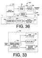
- FIG. 33 is a block diagram of an aspect of a digital controller including an energy saving discontinuous mode (ESDM).
- ESDM energy saving discontinuous mode
- FIG. 34A is a block diagram of an aspect of a digital controller for controlling the switchover between constant current mode and discontinuous current mode.
- FIG. 34B is a timing diagram of waveforms associated with an aspect of a digital controller.
- FIG. 35 is a flow diagram of an aspect of an operation for controlling the switchover between constant current mode and discontinuous current mode.
- the power arrays 114a and 114b each include one or more power switches operated in a switching mode, cycling between on and off states. Any type of power switch may be used such as MOSFETs, BJTs, IGBTs, and MCTs.
- the power arrays 114a and 114b may be configured in any topology such as buck, boost, flyback, sepic, Cuk, and zeta.
- the power arrays 114a and 114b are described in a buck configuration.
- the upper power array 114a is connected between Vin and a common node, VL.
- the lower power array 114b is connected between VL and a lower voltage such as ground.
- Vin and ground are applied to VL.
- Vin When Vin is applied to VL, energy flows from Vin through VL to an output filter (see Figure 1).
- Current sensors 116a and 116b may measure the current flowing through the power arrays 114a and 114b.
- the current sensors may employ any method of current sensing such as current transformers, series resistors, hall effect devices, and determining the current based on the voltage developed across a MOSFET in the on state.
- Each of the current sensors 116a and 116b may generate a digital output to indicate a current characteristic such as peak current, average current, and actual current.
- the digital output of the current may be one or more bits.
- a soft start circuit 124 may generate a soft start signal to limit the transfer of energy to the output during turn-on of the power supply.
- the soft start signal may be a 5 bit signal that controls the pulse width of the drive signals to limit energy transfer to the output. For example, during turn-on, the soft start signal may ramp up in value limiting the maximum pulse width. Any type of soft start technique may be employed such as limiting the duty cycle, controlling the operating frequency of the drive signals, and controllably increasing the reference voltage that the output feedback signal is compared to gradually increase the output voltage to a steady-state level.
- the soft start circuit 124 may limit the transfer of energy on a cycle by cycle basis.
- An adaptive duty limit 126 may generate a digital signal to limit the transfer of energy to the output as a function of an electrical characteristic of the input power such as Vin, the input current, lin, the input ripple voltage, VINripple, the input power, Pin, the input source impedance, Rs, and the input energy, Qin.
- the adaptive duty limit 126 may monitor lin and generate a digital signal to limit the duty cycle so that the amplitude of lin does not exceed a threshold value.
- the adaptive duty limit 126 may operate on a cycle-by-cycle basis to control the threshold value. Each cycle, the adaptive duty limit 126 may change the threshold value and limit the duty cycle for the next cycle. The duty cycle for the next cycle may be determined based on comparing the input power electrical characteristic of the previous cycle to the threshold value.
- a soft start signal is generated to limit energy transfer to the regulated output during turn-on.
- the soft-start signal limits the duty cycle over which the power arrays over driven.
- an input limit signal is generated to limit energy transfer to the regulated output as a function of the input power. For example, power transfer may be limited when the input voltage is less than a predetermined voltage or the input current is greater than a predetermined current.
- a clocked duty cycle may be generated.
- the clocked duty cycle is adjusted by time durations less than a clock pulse of the clock signal.
- Figure 5 shows an aspect of an adaptive multi-mode control system 300 for controlling an output regulator.
- the multi-mode control system 300 may automatically switch between three or more operating modes as a function of the regulated output.
- the output regulator may be any type of regulator including switching and linear, and regulate any output characteristic such as voltage and current.
- the multi-mode controller 300 may be configured to include any combination of operating modes such as hysteretic mode, adaptive hysteretic mode, pulse width modulated mode, constant on-time mode, constant off-time mode, resonant modes, fixed frequency soft-switching mode, voltage mode, current mode, fixed frequency, and variable frequency including combinations of the operating modes.
- the multi-mode controller 300 is implemented in a digital control system and operated with a clock signal.
- the adaptive multi-mode control system 300 may switch between operating modes on a cycle-by-cycle basis of the clock signal. Each clock cycle, one or more characteristics of the output regulator may be sensed, and then the operating mode be selected based on the sensed characteristics. Any output regulator characteristic may be used such as output voltage, output current, bias current, switch current, and temperature wherein each of the characteristics may be any mathematical form such as peak, average, weighted average, rate of change, and instantaneous.
- the adaptive multi-mode control system 300 may start in voltage-mode hysteretic control 302 when the switching regulator tums-on.
- Figure 6 shows a regulated output voltage 320 of the switching regulator during several operating states.
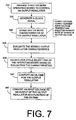
- Figure 7 shows an aspect of an adaptive multi-mode control system.
- three or more operating modes are provided for controlling an output regulator.
- the operating modes may be configured in any clock driven medium such as firmware, software, and hardware.
- a clock signal is generated for operating the multi-mode control system 300.
- one or more characteristics of the output regulator may be sensed.
- the output regulator characteristics may be sensed as a function of the clock cycle such as a number of clock cycles corresponding to a minimum on-time or duty cycle of the output regulator.
- the sensed output regulator characteristics may be evaluated to determine which operating mode to use.
- one of the operating modes may be selected based on the evaluation.
- FIG 8 shows an aspect of an output regulator 400 for generating a regulated output.
- the output regulator 400 may include a digital controller 402 to receive a feedback signal 404 and to generate one or more drive signals 406 to drive a power stage 408.
- the power stage 408 converts an unregulated voltage, such as Vin, to a chopped waveform that is filtered by an output filter 412 to generate a regulated output 414.
- the regulated output, Vout is preferably a DC output and may be regulated based on any output characteristic including voltage, current, and power.
- An output slicer 416 may generate the feedback signal 404 in response to sensing the output voltage.
- the output slicer 416 may determine a range of voltages within which the output voltage is included.
- the output slicer 416 may determine two or more voltage ranges to describe a combined range of voltages, and then determine the voltage range within which the output voltage is included. For example, a combined range of voltages extending from 0 volts to 10 volts may be described by a first voltage range from 0 volts to 8 volts, a second voltage range from 8 volts to 9 volts, a third voltage range from 9 volts to 10 volts, and a fourth voltage range being 10 volts and greater.
- the configuration of the voltage ranges may be changed such as from consecutive to overlapping.
- the output slicer 416 is described as having voltage references, current references may also be used to define current ranges to which a current may be compared.
- the output slicer 416 may compare the output voltage to the predetermined voltage ranges and select a digital value to represent the voltage range within which the output voltage is.
- the feedback signal 404 is a digital signal having two or more bits to represent the voltage range that corresponds to the output voltage, such as a digital bus carrying a decoded signal and separate digital lines to represent each voltage range.
- Figure 10 shows an aspect of a voltage slicer 450 for generating a digital value to represent a voltage range within which a sensed voltage is included.
- a reference generator 452 may generate several voltage references 454 for setting voltage limits for each of the voltage ranges. There may be any arrangement of voltage references such as assigning individual voltage references 454 for each voltage limit and deriving multiple voltage limits from a single voltage reference.
- a control signal 455 may dynamically control the voltage references so that the voltage limits may be controlled on a cycle-by-cycle basis at the sampling frequency.
- the control signal 455 may control one or more of the voltage references and switch the voltage references between two or more voltage levels.
- the control signal 455 may be analog, digital, mixed-signal, parallel, serial, one or more lines and combinations thereof.
- One or more comparators 456 may compare the output voltage to the voltage limits 454. When multiple comparators 456 are used, the comparators may operate in parallel to compare the output voltage to each of the voltage limits defining voltage ranges. In one alternative, a single comparator 456 may be used to compare the output voltage with a controlled voltage reference that may be sequenced on clock transitions through values corresponding to the voltage limits.
- An encoder 458 may encode the outputs of the comparators 450 to a digital signal having two or more bits.
- the digital signal may be any format such as parallel and serial.
- Figure 11 shows an operation of a voltage slicer.
- three or more reference levels may be generated to define voltage ranges.
- the reference levels may be static or dynamic.
- Static reference levels may be maintained at a constant level.
- Dynamic reference levels may controlled on a cycle-by-cycle basis so that the voltage ranges may be changed dynamically. For example, during turn-on of a power regulator when the regulator output is increasing, the voltage ranges may be set to be 10% of the steady-state level of the power regulator output. Then, when the power regulator output begins to settle towards the steady-state level, the voltage ranges may be decreased to 5% of the steady-state level.
- the level of a device characteristic may be sensed.
- FIG 12A shows an aspect of a power array 500 to generate a chopped voltage from an input voltage.
- the power array 500 may be included in a power regulator such as power regulator 10 described in this specification.
- the power array 500 may include one or more switch arrays 502a and 502b of power switches Q1-Q8 to control the flow of energy between two nodes.
- the power switches Q1-Q8 may each operate independently in two states, an on state and an off state. In the on state, the power switch has a low impedance and conducts energy between the two nodes. In the off state, the power switch has a high impedance and blocks the flow of energy between the two nodes.
- the power switches Q1-Q8 may include any mixture of sizes such as for MOSFETs, one device may have an Rds(on) of 0.1 ohm while other devices have an Rds(on) of 0.2 ohm and 0.4 ohm respectively.
- the switch arrays 502a and 502b may be connected as any topology such as buck, boost, flyback, Cuk, sepic, and zeta.
- the switch arrays 502a and 502b are connected as a buck topology in which the upper switch array 502a conducts energy during a conduction period and the lower switch array 502b conducts energy during a free-wheeling period.
- the switch arrays 502a and 502b may comprise any combination of power switches such as MOSFETs, BJTs, MCTs, IGBTs, and RF FETs.
- a switch controller 504 generates drive signals for controlling the power switches Q1-Q8.
- the switch controller 504 operates digitally and may be implemented as any form of digital entity such as digital circuitry, and a programmable device executing software or firmware.
- the switch controller 504 may receive a duty cycle signal 508 and generate the drive signals based on the duty cycle signal 508.
- the switch controller 504 may operate on a cycle-by-cycle basis at the sampling frequency to determine the drive signals.
- the sampling frequency may be 20 times or more higher than the switching frequency of the output regulator. For example, during fixed frequency operation the output regulator may operate between 50 kHz and 1 MHz while the sampling frequency may range between 1 MHz and 100 MHz.
- the switch controller 504 may determine the drive signals each clock cycle corresponding to the sampling frequency.
- Each of the power switches Q1-Q8 may be independently enabled or disabled on a cycle-by-cycle basis.
- the quantity of power switches within a switch array that are enabled may be controlled.
- the quantity of enabled/disabled power switches Q1-Q8 may be determined on the basis of any operating characteristic such as output current, ambient temperature, operating temperature, output voltage, and inductor current. For example, when the output current is equal to about half of the maximum output current, only two of four power switches in each switch array may be enabled so that the switching losses of the power switches are minimized.
- additional power switches may be enabled to reduce conduction losses.
- the quantity of power switches may be increased or decreased, thereby for example reducing switching and conduction losses.
- the switch controller 504 may control each of the power switches Q1-Q8 independently via the drive signals so that the time relationship between each of the power switches during transitions between the on and off states may be controlled cycle-by-cycle.
- the time sequence of the on and off transitions of the power switches Q1-Q4 and Q5-Q8 within each of the switch arrays 502a and 502b may be individually controlled. For example, referring to Figure 13, which shows waveforms associated with an aspect of the power array 500, an off state to on state transition 520 of the power switches Q1-Q4 may be controlled so that first Q4 turns off, followed by Q2 and Q3 together, and finally Q1.
- Figure 13 shows an aspect of a current sensing operation of the power array 500.
- a sampling waveform, SMPL, 524 shows an exemplary sampling rate.
- Waveforms 526-540 show a portion of a conduction cycle for the power switches Q1-Q8.
- Waveform 542 shows current flowing through an output inductor. The current in the inductor decreases at a linear rate during a freewheeling portion of the conduction cycle of the power array 500.
- Waveform 544 shows a sense voltage.
- the sense voltage may be equal to a sense impedance times a sense current corresponding to the current flowing through the output inductor.
- the resolution of the sense voltage may be adjusted on a cycle-by-cycle basis at the sampling frequency.
- An encircled portion 546 of the sense voltage waveform 544 shows the resolution of the sense voltage being increased as the inductor current decreases in amplitude.
- the power array 500 zooms in to increase the resolution of the sensed current.
- the resolution may be controlled in any manner on a cycle-by-cycle basis at the sampling frequency.
- the resolution may be controlled by amplifying the sense current signal based on a resolution trigger such as the sense current amplitude, the quantity of power switches that are enabled, and a predetermined time in the conduction cycle.
- the resolution may be controlled by controlling the impedance of the current sensing device such as by; 1) sensing current across the ON impedance of the power switches and 2) controlling the quantity of power switches that operate in parallel during the conduction cycle.
- the impedance of the sensing device such as a resistor may be controlled.
- the resolution may be controlled at the sampling frequency throughout the conduction cycle so that as the amplitude of the sensed current decreases, the power array 500 may zoom in during the conduction cycle to increase the resolution.
- Figure 16 shows an aspect of a diode emulation system 600 for emulating a free-wheeling diode of an output regulator that operates as a switching regulator.
- the output regulator includes an output filter 605.
- the diode emulation system 600 is shown in a buck topology with a ground referenced output, any topology may be used such as boost, buck-boost, cuk, sepic, and zeta, and the output may be referenced to any circuit node such as high-side reference and low-side reference.
- the diode emulation system 600 advantageously uses a free-wheeling switch array 602 to emulate a free-wheeling diode of the output regulator.
- the freewheeling switch array 602 may include several power switches connected in parallel and independently controlled.
- the voltage reference may be programmable on a cycle-by-cycle basis so that for example, the lower current sense circuit threshold value may be adjusted to account for variations in the impedance of the freewheeling switch array 602 such as changes in the quantity of parallel power switches and temperature effects.
- the power switches of the freewheeling switch array 602 may be switched to the on-state as the first power switch 604 is switched to the off-state based on a pulse width signal.
- the freewheeling switch array 602 may be inhibited from changing operating state to the on-state.
- the operating state of the freewheeling switch array 602 may be changed from the on-state to the off-state.
- the power switches of the freewheeling switch array 602 may be switched to the off-state as a function of the pulse width signal.
- step 706 compare the current flowing through the first power switch to a reference level.
- step 708 a delay having a predetermined time period beginning when the current flowing through the power switch decreases to less than the reference level may be generated.
- step 710 change the operating state of the other power switch from the off-state to the on-state.
- the expected power losses for the power switches may be determined using operating conditions such as Vds, Ids, and Rds(on) of the power switches to compute the expected power losses.
- the expected power losses may also be determined using a lookup mechanism such as a lookup table to estimate the expected power losses.
- the lookup mechanism may cross reference ranges of operating conditions to estimated power losses.
- the lookup mechanism may also indicate a preferred set of power switches to enable for particular operating conditions.
- the expected power losses may be determined on a cycle-by-cycle basis to obtain expected losses such as estimated losses and computed losses.
- an upper switch array having four power switches in parallel may be operated so that the four power switches are sequentially turned-off one-by-one so that the impedance of the common node may change from a low impedance to a high impedance over a controlled time period, thereby damping noise spikes occurring during the switch transition.
- the power switch pairs may be any type of cascode connected power switches having a variable output capacitance such as MOSFETs with BJTs, MOSFETs with IGBTs, and MOSFETs with MCTs.
- Controlling the capacitance of the common node may be particularly advantageous in resonant mode, soft switching, and quasi-resonant mode switching regulators. For example, controlling the capacitance of the common node in a fixed frequency soft switching regulator may control the resonance of the power switches over increased input voltage and output load ranges.
- monitor the current flowing through a switch array The switch array current may be monitored directly or indirectly such as by monitoring the output current of the output regulator.
- Figure 34A shows an aspect of a digital controller 1100 for controlling the transition between switching modes of an output regulator.
- the digital controller 1100 may control switching between continuous current mode (CCM) operation and discontinuous current mode (DCM) operation.
- Figure 34B shows waveforms associated with DCM operation.
- a first waveform, Vout, 1110 shows a regulated output voltage of the output regulator.
- a second waveform shows an inductor current, IL, 1112 of the output regulator.
- the regulated output voltage 1110 and the inductor current 1112 operate in three phases; a conduction phase, a freewheeling phase, and a discontinuous phase.
- Figure 36 shows a storage system 1200 for capturing state information of a digital controller 1201 for an output regulator 1200.
- the output regulator 1200 may be any type of regulator including a switching regulator, linear regulator, current regulator, voltage regulator, and power regulator.
- the output regulator 1200 may include a power stage 1204 and output filter 1206 to convert energy from in input source to a regulated output for supplying energy to a load 1208.
- An output sensor 1210 may sense the regulated output and provide an input to the digital controller 1201.
Landscapes
- Engineering & Computer Science (AREA)
- Power Engineering (AREA)
- Dc-Dc Converters (AREA)
- Control Of Eletrric Generators (AREA)
- Control Of Voltage And Current In General (AREA)
- Manipulation Of Pulses (AREA)
- Measurement Of Current Or Voltage (AREA)
Applications Claiming Priority (7)
| Application Number | Priority Date | Filing Date | Title |
|---|---|---|---|
| US39511502P | 2002-07-10 | 2002-07-10 | |
| US395115P | 2002-07-10 | ||
| US39569702P | 2002-07-12 | 2002-07-12 | |
| US395697P | 2002-07-12 | ||
| US460825 | 2003-06-12 | ||
| US10/460,825 US6977492B2 (en) | 2002-07-10 | 2003-06-12 | Output regulator |
| EP03763431A EP1532501B1 (de) | 2002-07-10 | 2003-07-10 | Digitale Steuerung für einen Ausgangsregler |
Related Parent Applications (2)
| Application Number | Title | Priority Date | Filing Date |
|---|---|---|---|
| EP03763431.8 Division | 2003-07-10 | ||
| EP03763431A Division EP1532501B1 (de) | 2002-07-10 | 2003-07-10 | Digitale Steuerung für einen Ausgangsregler |
Publications (3)
| Publication Number | Publication Date |
|---|---|
| EP1524572A2 true EP1524572A2 (de) | 2005-04-20 |
| EP1524572A3 EP1524572A3 (de) | 2005-11-02 |
| EP1524572B1 EP1524572B1 (de) | 2011-12-28 |
Family
ID=34382067
Family Applications (9)
| Application Number | Title | Priority Date | Filing Date |
|---|---|---|---|
| EP04023259A Expired - Lifetime EP1524575B1 (de) | 2002-07-10 | 2003-07-10 | Ausgangsregler |
| EP04023258A Expired - Lifetime EP1524574B1 (de) | 2002-07-10 | 2003-07-10 | Ausgangsregler |
| EP04023251A Expired - Fee Related EP1524571B1 (de) | 2002-07-10 | 2003-07-10 | Steuerungssystem für einen Ausgangsregler |
| EP04023256A Expired - Lifetime EP1524572B1 (de) | 2002-07-10 | 2003-07-10 | Spannungsversorgungsanordnung und Verfahren |
| EP04023249A Expired - Lifetime EP1524570B1 (de) | 2002-07-10 | 2003-07-10 | Adaptive Regelschleife |
| EP04023234A Expired - Lifetime EP1524568B1 (de) | 2002-07-10 | 2003-07-10 | Adaptiver Tastverhältnisbegrenzer |
| EP04023192A Expired - Fee Related EP1524567B1 (de) | 2002-07-10 | 2003-07-10 | Tastverhältnisschätzer |
| EP04023247A Expired - Fee Related EP1524569B1 (de) | 2002-07-10 | 2003-07-10 | Tastverhältnisschätzer |
| EP04023257A Expired - Fee Related EP1524573B1 (de) | 2002-07-10 | 2003-07-10 | Steuerungssystem für einen Ausgangsregler |
Family Applications Before (3)
| Application Number | Title | Priority Date | Filing Date |
|---|---|---|---|
| EP04023259A Expired - Lifetime EP1524575B1 (de) | 2002-07-10 | 2003-07-10 | Ausgangsregler |
| EP04023258A Expired - Lifetime EP1524574B1 (de) | 2002-07-10 | 2003-07-10 | Ausgangsregler |
| EP04023251A Expired - Fee Related EP1524571B1 (de) | 2002-07-10 | 2003-07-10 | Steuerungssystem für einen Ausgangsregler |
Family Applications After (5)
| Application Number | Title | Priority Date | Filing Date |
|---|---|---|---|
| EP04023249A Expired - Lifetime EP1524570B1 (de) | 2002-07-10 | 2003-07-10 | Adaptive Regelschleife |
| EP04023234A Expired - Lifetime EP1524568B1 (de) | 2002-07-10 | 2003-07-10 | Adaptiver Tastverhältnisbegrenzer |
| EP04023192A Expired - Fee Related EP1524567B1 (de) | 2002-07-10 | 2003-07-10 | Tastverhältnisschätzer |
| EP04023247A Expired - Fee Related EP1524569B1 (de) | 2002-07-10 | 2003-07-10 | Tastverhältnisschätzer |
| EP04023257A Expired - Fee Related EP1524573B1 (de) | 2002-07-10 | 2003-07-10 | Steuerungssystem für einen Ausgangsregler |
Country Status (1)
| Country | Link |
|---|---|
| EP (9) | EP1524575B1 (de) |
Cited By (2)
| Publication number | Priority date | Publication date | Assignee | Title |
|---|---|---|---|---|
| GB2524065A (en) * | 2014-03-13 | 2015-09-16 | Tdk Lambda Uk Ltd | Converter |
| KR101945350B1 (ko) | 2017-05-26 | 2019-02-07 | 엘에스산전 주식회사 | 전력 변환 장치의 설계 방법 |
Families Citing this family (21)
| Publication number | Priority date | Publication date | Assignee | Title |
|---|---|---|---|---|
| US8031492B2 (en) * | 2007-06-14 | 2011-10-04 | System General Corp. | PWM controller for compensating a maximum output power of a power converter |
| CN102150093B (zh) * | 2008-09-11 | 2013-12-25 | 马维尔国际贸易有限公司 | 智能切换控制器和功率转换电路和方法 |
| US8285502B2 (en) | 2008-11-21 | 2012-10-09 | L&L Engineering, Llc | Digital compensator for power supply applications |
| WO2010076671A1 (en) * | 2009-01-05 | 2010-07-08 | Freescale Semiconductor, Inc. | Current sensing circuitry and integrated circuit and method for sensing a current |
| US9134348B2 (en) | 2009-04-16 | 2015-09-15 | Panoramic Power Ltd. | Distributed electricity metering system |
| GB2498884B (en) | 2009-04-16 | 2014-02-12 | Panoramic Power Ltd | Apparatus and methods thereof for power consumption measurement at circuit breaker points |
| US9678114B2 (en) | 2009-04-16 | 2017-06-13 | Panoramic Power Ltd. | Apparatus and methods thereof for error correction in split core current transformers |
| MX2012002973A (es) | 2009-09-09 | 2012-04-19 | Du Pont | Derivados de pirimidona herbicidas. |
| US8829879B2 (en) | 2010-12-03 | 2014-09-09 | Maxim Integrated Products, Inc. | Inductor current measurement for DC to DC converters |
| CN103425170A (zh) | 2012-05-22 | 2013-12-04 | 联合聚晶股份有限公司 | 自适应负载变化的电源供应电路 |
| DE102012217898B4 (de) * | 2012-10-01 | 2016-11-24 | Continental Automotive Gmbh | Verfahren und Vorrichtung zum Betreiben eines Gleichspannungswandlers |
| TWI502302B (zh) * | 2013-10-16 | 2015-10-01 | Ind Tech Res Inst | 穩壓器及其控制方法 |
| CN104571253B (zh) | 2013-10-16 | 2016-04-27 | 财团法人工业技术研究院 | 稳压器及其控制方法 |
| EP2894776B1 (de) * | 2014-01-09 | 2017-11-29 | Dialog Semiconductor (UK) Limited | Gleichspannungswandler für hohe Spannungen mit Master/Slave Tiefsetzstellerausgangsstufen |
| EP2894777A1 (de) | 2014-01-09 | 2015-07-15 | Dialog Semiconductor (UK) Limited | Gleichspannungswandlereffizienzsteigerung für niedrige Stromwerte |
| US9698691B2 (en) | 2015-06-04 | 2017-07-04 | Dialog Semiconductor (Uk) Limited | Circuit and method for maximum duty cycle limitation in switching converters |
| US10024885B2 (en) | 2015-07-28 | 2018-07-17 | Panoramic Power Ltd. | Thermal management of self-powered power sensors |
| US9891252B2 (en) | 2015-07-28 | 2018-02-13 | Panoramic Power Ltd. | Thermal management of self-powered power sensors |
| US9698681B2 (en) | 2015-09-30 | 2017-07-04 | Dialog Semiconductor (Uk) Limited | Circuit and method for maximum duty cycle limitation in step up converters |
| CN111342652B (zh) * | 2020-03-02 | 2021-05-14 | 启攀微电子(上海)有限公司 | 一种低待机功耗的电荷泵电路结构 |
| US10897251B1 (en) * | 2020-04-20 | 2021-01-19 | Infineon Technologies Austria Ag | Isolation barrier communication system in a package for isolated gate driver communication |
Family Cites Families (20)
| Publication number | Priority date | Publication date | Assignee | Title |
|---|---|---|---|---|
| FR2656930B1 (fr) * | 1990-01-05 | 1992-10-02 | Alcatel Radiotelephone | Circuit de mesure numerique d'un signal electrique. |
| JP3185257B2 (ja) * | 1991-07-23 | 2001-07-09 | 株式会社明電舎 | 電力変換ユニットの並列運転装置 |
| US5563779A (en) * | 1994-12-05 | 1996-10-08 | Motorola, Inc. | Method and apparatus for a regulated supply on an integrated circuit |
| US5949226A (en) * | 1995-04-10 | 1999-09-07 | Kabushiki Kaisha Toyoda Jidoshokki Seisakush | DC/DC converter with reduced power consumpton and improved efficiency |
| CN1052586C (zh) * | 1996-06-24 | 2000-05-17 | Tdk株式会社 | 开关电源装置及其数字控制装置 |
| US6020729A (en) * | 1997-12-16 | 2000-02-01 | Volterra Semiconductor Corporation | Discrete-time sampling of data for use in switching regulators |
| JP3744680B2 (ja) * | 1998-03-31 | 2006-02-15 | 富士通株式会社 | 電源装置、および電源回路の制御方法 |
| JP2000163961A (ja) * | 1998-11-26 | 2000-06-16 | Mitsubishi Electric Corp | 同期型半導体集積回路装置 |
| DE19909464C2 (de) * | 1999-03-04 | 2001-03-22 | Danfoss Compressors Gmbh | Verfahren zur Erzeugung einer geregelten Gleichspannung aus einer Wechselspannung und Stromversorgungseinrichtung zur Durchführung des Verfahrens |
| US6232754B1 (en) * | 1999-08-15 | 2001-05-15 | Philips Electronics North America Corporation | Sleep-mode-ready switching power converter |
| US6215288B1 (en) * | 2000-02-25 | 2001-04-10 | Cadence Design Systems, Inc. | Ultra-low power switching regulator method and apparatus |
| JP2001258269A (ja) * | 2000-03-15 | 2001-09-21 | Kawasaki Steel Corp | ソフトスイッチングdc−dcコンバータ |
| US20020057080A1 (en) * | 2000-06-02 | 2002-05-16 | Iwatt | Optimized digital regulation of switching power supply |
| US6525514B1 (en) * | 2000-08-08 | 2003-02-25 | Power Integrations, Inc. | Method and apparatus for reducing audio noise in a switching regulator |
| US6577109B2 (en) * | 2000-08-25 | 2003-06-10 | Synqor, Inc. | Interleaved power converters incorporating bang-bang control |
| EP1325547A2 (de) * | 2000-10-13 | 2003-07-09 | Primarion, Inc. | Verfahren und vorrichtung zur hochphasenleistungsregelung |
| US6304067B1 (en) * | 2000-12-08 | 2001-10-16 | Micrel, Incorporated | Adding a laplace transform zero to a linear integrated circuit for frequency stability |
| US6445169B1 (en) * | 2000-12-29 | 2002-09-03 | Volterra Semiconductor Corporation | Lag compensating controller having an improved transient response |
| US6631064B2 (en) * | 2001-02-06 | 2003-10-07 | Semiconductor Components Industries Llc | Apparatus and method for providing overcurrent protection for switch-mode power supplies |
| AU2002320142A1 (en) * | 2001-06-21 | 2003-01-08 | Champion Microelectronic Corp. | Current limiting technique for a switching power converter |
-
2003
- 2003-07-10 EP EP04023259A patent/EP1524575B1/de not_active Expired - Lifetime
- 2003-07-10 EP EP04023258A patent/EP1524574B1/de not_active Expired - Lifetime
- 2003-07-10 EP EP04023251A patent/EP1524571B1/de not_active Expired - Fee Related
- 2003-07-10 EP EP04023256A patent/EP1524572B1/de not_active Expired - Lifetime
- 2003-07-10 EP EP04023249A patent/EP1524570B1/de not_active Expired - Lifetime
- 2003-07-10 EP EP04023234A patent/EP1524568B1/de not_active Expired - Lifetime
- 2003-07-10 EP EP04023192A patent/EP1524567B1/de not_active Expired - Fee Related
- 2003-07-10 EP EP04023247A patent/EP1524569B1/de not_active Expired - Fee Related
- 2003-07-10 EP EP04023257A patent/EP1524573B1/de not_active Expired - Fee Related
Non-Patent Citations (1)
| Title |
|---|
| None |
Cited By (3)
| Publication number | Priority date | Publication date | Assignee | Title |
|---|---|---|---|---|
| GB2524065A (en) * | 2014-03-13 | 2015-09-16 | Tdk Lambda Uk Ltd | Converter |
| GB2524065B (en) * | 2014-03-13 | 2021-03-03 | Tdk Lambda Uk Ltd | Converter |
| KR101945350B1 (ko) | 2017-05-26 | 2019-02-07 | 엘에스산전 주식회사 | 전력 변환 장치의 설계 방법 |
Also Published As
| Publication number | Publication date |
|---|---|
| EP1524568B1 (de) | 2008-10-15 |
| EP1524574A2 (de) | 2005-04-20 |
| EP1524572B1 (de) | 2011-12-28 |
| EP1524574B1 (de) | 2010-09-08 |
| EP1524569A2 (de) | 2005-04-20 |
| EP1524571A3 (de) | 2005-08-31 |
| EP1524575A2 (de) | 2005-04-20 |
| EP1524573A3 (de) | 2005-06-01 |
| EP1524568A2 (de) | 2005-04-20 |
| EP1524573B1 (de) | 2011-04-20 |
| EP1524569A3 (de) | 2005-08-17 |
| EP1524571B1 (de) | 2011-04-20 |
| EP1524572A3 (de) | 2005-11-02 |
| EP1524569B1 (de) | 2008-09-10 |
| EP1524575B1 (de) | 2011-04-20 |
| EP1524574A3 (de) | 2005-06-01 |
| EP1524568A3 (de) | 2005-08-17 |
| EP1524570A3 (de) | 2005-08-03 |
| EP1524567B1 (de) | 2008-09-10 |
| EP1524570B1 (de) | 2008-09-10 |
| EP1524567A3 (de) | 2005-08-17 |
| EP1524571A2 (de) | 2005-04-20 |
| EP1524575A3 (de) | 2005-08-31 |
| EP1524573A2 (de) | 2005-04-20 |
| EP1524570A2 (de) | 2005-04-20 |
| EP1524567A2 (de) | 2005-04-20 |
Similar Documents
| Publication | Publication Date | Title |
|---|---|---|
| EP1532501B1 (de) | Digitale Steuerung für einen Ausgangsregler | |
| EP1524573B1 (de) | Steuerungssystem für einen Ausgangsregler |
Legal Events
| Date | Code | Title | Description |
|---|---|---|---|
| PUAI | Public reference made under article 153(3) epc to a published international application that has entered the european phase |
Free format text: ORIGINAL CODE: 0009012 |
|
| 17P | Request for examination filed |
Effective date: 20040929 |
|
| AK | Designated contracting states |
Kind code of ref document: A2 Designated state(s): AT BE BG CH CY CZ DE DK EE ES FI FR GB GR HU IE IT LI LU MC NL PT RO SE SI SK TR |
|
| RIC1 | Information provided on ipc code assigned before grant |
Ipc: 7H 02M 3/158 B Ipc: 7G 05F 1/618 B Ipc: 7H 02M 3/335 B Ipc: 7G 05F 1/565 A |
|
| PUAL | Search report despatched |
Free format text: ORIGINAL CODE: 0009013 |
|
| RIC1 | Information provided on ipc code assigned before grant |
Ipc: 7H 02M 3/158 B Ipc: 7G 01R 19/00 B Ipc: 7G 05F 1/618 B Ipc: 7G 05F 1/565 A Ipc: 7H 02M 3/335 B |
|
| AK | Designated contracting states |
Kind code of ref document: A3 Designated state(s): AT BE BG CH CY CZ DE DK EE ES FI FR GB GR HU IE IT LI LU MC NL PT RO SE SI SK TR |
|
| AKX | Designation fees paid |
Designated state(s): DE FR GB |
|
| 17Q | First examination report despatched |
Effective date: 20070130 |
|
| GRAP | Despatch of communication of intention to grant a patent |
Free format text: ORIGINAL CODE: EPIDOSNIGR1 |
|
| GRAS | Grant fee paid |
Free format text: ORIGINAL CODE: EPIDOSNIGR3 |
|
| GRAA | (expected) grant |
Free format text: ORIGINAL CODE: 0009210 |
|
| AC | Divisional application: reference to earlier application |
Ref document number: 1532501 Country of ref document: EP Kind code of ref document: P |
|
| AK | Designated contracting states |
Kind code of ref document: B1 Designated state(s): DE FR GB |
|
| REG | Reference to a national code |
Ref country code: GB Ref legal event code: FG4D |
|
| REG | Reference to a national code |
Ref country code: DE Ref legal event code: R096 Ref document number: 60339576 Country of ref document: DE Effective date: 20120308 |
|
| PLBE | No opposition filed within time limit |
Free format text: ORIGINAL CODE: 0009261 |
|
| STAA | Information on the status of an ep patent application or granted ep patent |
Free format text: STATUS: NO OPPOSITION FILED WITHIN TIME LIMIT |
|
| 26N | No opposition filed |
Effective date: 20121001 |
|
| REG | Reference to a national code |
Ref country code: DE Ref legal event code: R097 Ref document number: 60339576 Country of ref document: DE Effective date: 20121001 |
|
| REG | Reference to a national code |
Ref country code: FR Ref legal event code: PLFP Year of fee payment: 14 |
|
| REG | Reference to a national code |
Ref country code: FR Ref legal event code: PLFP Year of fee payment: 15 |
|
| REG | Reference to a national code |
Ref country code: FR Ref legal event code: PLFP Year of fee payment: 16 |
|
| PGFP | Annual fee paid to national office [announced via postgrant information from national office to epo] |
Ref country code: CH Payment date: 20180719 Year of fee payment: 10 |
|
| PG25 | Lapsed in a contracting state [announced via postgrant information from national office to epo] |
Ref country code: FR Free format text: LAPSE BECAUSE OF NON-PAYMENT OF DUE FEES Effective date: 20190731 |
|
| REG | Reference to a national code |
Ref country code: DE Ref legal event code: R082 Ref document number: 60339576 Country of ref document: DE Representative=s name: GRUENECKER PATENT- UND RECHTSANWAELTE PARTG MB, DE Ref country code: DE Ref legal event code: R081 Ref document number: 60339576 Country of ref document: DE Owner name: MARVELL ASIA PTE, LTD., SG Free format text: FORMER OWNER: MARVELL WORLD TRADE LTD., ST. MICHAEL, BB |
|
| REG | Reference to a national code |
Ref country code: GB Ref legal event code: 732E Free format text: REGISTERED BETWEEN 20210805 AND 20210811 |
|
| PGFP | Annual fee paid to national office [announced via postgrant information from national office to epo] |
Ref country code: GB Payment date: 20220719 Year of fee payment: 20 Ref country code: DE Payment date: 20220727 Year of fee payment: 20 |
|
| P01 | Opt-out of the competence of the unified patent court (upc) registered |
Effective date: 20230508 |
|
| REG | Reference to a national code |
Ref country code: DE Ref legal event code: R071 Ref document number: 60339576 Country of ref document: DE |
|
| REG | Reference to a national code |
Ref country code: GB Ref legal event code: PE20 Expiry date: 20230709 |
|
| PG25 | Lapsed in a contracting state [announced via postgrant information from national office to epo] |
Ref country code: GB Free format text: LAPSE BECAUSE OF EXPIRATION OF PROTECTION Effective date: 20230709 |