EP1523697B1 - Procede de production de structure de laque photosensible - Google Patents
Procede de production de structure de laque photosensible Download PDFInfo
- Publication number
- EP1523697B1 EP1523697B1 EP03765041A EP03765041A EP1523697B1 EP 1523697 B1 EP1523697 B1 EP 1523697B1 EP 03765041 A EP03765041 A EP 03765041A EP 03765041 A EP03765041 A EP 03765041A EP 1523697 B1 EP1523697 B1 EP 1523697B1
- Authority
- EP
- European Patent Office
- Prior art keywords
- photoresist
- production
- volume
- structures according
- light beams
- Prior art date
- Legal status (The legal status is an assumption and is not a legal conclusion. Google has not performed a legal analysis and makes no representation as to the accuracy of the status listed.)
- Expired - Lifetime
Links
Images

Classifications
-
- G—PHYSICS
- G03—PHOTOGRAPHY; CINEMATOGRAPHY; ANALOGOUS TECHNIQUES USING WAVES OTHER THAN OPTICAL WAVES; ELECTROGRAPHY; HOLOGRAPHY
- G03F—PHOTOMECHANICAL PRODUCTION OF TEXTURED OR PATTERNED SURFACES, e.g. FOR PRINTING, FOR PROCESSING OF SEMICONDUCTOR DEVICES; MATERIALS THEREFOR; ORIGINALS THEREFOR; APPARATUS SPECIALLY ADAPTED THEREFOR
- G03F7/00—Photomechanical, e.g. photolithographic, production of textured or patterned surfaces, e.g. printing surfaces; Materials therefor, e.g. comprising photoresists; Apparatus specially adapted therefor
- G03F7/70—Microphotolithographic exposure; Apparatus therefor
- G03F7/70216—Mask projection systems
-
- B—PERFORMING OPERATIONS; TRANSPORTING
- B82—NANOTECHNOLOGY
- B82Y—SPECIFIC USES OR APPLICATIONS OF NANOSTRUCTURES; MEASUREMENT OR ANALYSIS OF NANOSTRUCTURES; MANUFACTURE OR TREATMENT OF NANOSTRUCTURES
- B82Y20/00—Nanooptics, e.g. quantum optics or photonic crystals
-
- G—PHYSICS
- G02—OPTICS
- G02B—OPTICAL ELEMENTS, SYSTEMS OR APPARATUS
- G02B6/00—Light guides; Structural details of arrangements comprising light guides and other optical elements, e.g. couplings
- G02B6/10—Light guides; Structural details of arrangements comprising light guides and other optical elements, e.g. couplings of the optical waveguide type
- G02B6/12—Light guides; Structural details of arrangements comprising light guides and other optical elements, e.g. couplings of the optical waveguide type of the integrated circuit kind
- G02B6/122—Basic optical elements, e.g. light-guiding paths
- G02B6/1225—Basic optical elements, e.g. light-guiding paths comprising photonic band-gap structures or photonic lattices
-
- G—PHYSICS
- G02—OPTICS
- G02B—OPTICAL ELEMENTS, SYSTEMS OR APPARATUS
- G02B6/00—Light guides; Structural details of arrangements comprising light guides and other optical elements, e.g. couplings
- G02B6/10—Light guides; Structural details of arrangements comprising light guides and other optical elements, e.g. couplings of the optical waveguide type
- G02B6/12—Light guides; Structural details of arrangements comprising light guides and other optical elements, e.g. couplings of the optical waveguide type of the integrated circuit kind
- G02B2006/12083—Constructional arrangements
- G02B2006/12107—Grating
-
- G—PHYSICS
- G02—OPTICS
- G02B—OPTICAL ELEMENTS, SYSTEMS OR APPARATUS
- G02B6/00—Light guides; Structural details of arrangements comprising light guides and other optical elements, e.g. couplings
- G02B6/10—Light guides; Structural details of arrangements comprising light guides and other optical elements, e.g. couplings of the optical waveguide type
- G02B6/12—Light guides; Structural details of arrangements comprising light guides and other optical elements, e.g. couplings of the optical waveguide type of the integrated circuit kind
- G02B2006/12166—Manufacturing methods
- G02B2006/12173—Masking
-
- G—PHYSICS
- G03—PHOTOGRAPHY; CINEMATOGRAPHY; ANALOGOUS TECHNIQUES USING WAVES OTHER THAN OPTICAL WAVES; ELECTROGRAPHY; HOLOGRAPHY
- G03H—HOLOGRAPHIC PROCESSES OR APPARATUS
- G03H2223/00—Optical components
- G03H2223/25—Index matching material
-
- G—PHYSICS
- G03—PHOTOGRAPHY; CINEMATOGRAPHY; ANALOGOUS TECHNIQUES USING WAVES OTHER THAN OPTICAL WAVES; ELECTROGRAPHY; HOLOGRAPHY
- G03H—HOLOGRAPHIC PROCESSES OR APPARATUS
- G03H2250/00—Laminate comprising a hologram layer
- G03H2250/12—Special arrangement of layers
Definitions
- the invention relates to methods for producing structures in a volume of photoresist (photoresist volume).
- the US 3,635,540 A and the GB 1 289 095 A each disclose a method for producing holograms with two light beams which are superimposed in a volume, which previously run through a transparent optical element in the form of a Dahlflächners (prism, rhombus).
- photoresist structures To produce photoresist structures, according to the in the WO 01/22133 A1 described a so-called holographic lithography, a photosensitive material with a multi-beam interference pattern resulting from the superposition of multiple light beams, exposed and then developed.
- the shape of the photoresist patterns thus produced generally depends on the angles of the interfering light rays inside the photoresist.
- the use of a transparent optical element and, if necessary, the use of immersion substance between solid optical elements is proposed there.
- the invention has for its object to produce a greater variety of photoresist structures.
- the maximum achievable angle of refraction of a beam when irradiated from the outer medium is the limit angle of total reflection, which assumes a value of about 36 ° in air and typical photoresists. This value would require grazing incidence. Angle inside the photoresist, which are larger than the critical angle of total reflection, can therefore not be adjusted by selecting the direction of irradiation.
- a photoresist volume is exposed with two, three, four, five, six or more light beams superimposed within the photoresist volume to create an interference pattern therein, with at least two exposures of the photoresist volume being provided between two light beams
- two or more exposures of the resist volume between which the light beams (and the photoresist volume are moved relative to one another) may be performed. whereby a photoresist pattern corresponding to the interference pattern is generated.
- the two, three, four, five, six or more partially coherent light beams are guided into the photoresist volume or out of the photoresist volume via a Dahlflächner.
- This makes it possible to make beam angles inside the photoresist beyond the critical angle of total reflection accessible, ie angles between the beams in the interior of the photoresist, which are not accessible by direct irradiation from the outer medium. In the case of air as an external medium, this is the considerable value range between approximately 36 ° and 90 °.
- the optical elements are configured as Kreflächner, preferably as a partial prism, preferably as a pyramid, particularly preferably as a truncated pyramid, or in a further embodiment as a spherical section.
- the photoresist can be applied directly to the optical element.
- an immersion substance is introduced between the optical element and the photoresist volume. If the photoresist is exposed in a liquid state, the immersion substance may be omitted.
- a particular advantage of the method according to the invention is that not only a few selected but all Bravais lattices can be produced. This is especially true for the cubic face centered (fcc) structure of interest for a three-dimensional full bandgap (see K. Busch, S. John, PRE 1998, 58, p. 3896).
- the refractive index difference between air and photoresist (1 and 1.6 in photoresist SU-8, respectively) is believed to be insufficient to achieve a full three-dimensional bandgap in the photonic crystal.
- the complementary structure of high refractive index material can be fabricated.
- both the pores and the photoresist skeleton are contiguous.
- the pores must be connected to each other so that on the one hand the unpolymerized photoresist can be dissolved out and on the other hand the pores can be continuously filled (infiltrated) with high refractive index material.
- the photoresist structure must be continuous so that it is mechanically stable and does not fall apart.
- photoresist structures according to the invention are suitable as an effect coating of surfaces, as a particle filter, as a micromixer, as a volume lattice, as a diffraction structure or dispersive structure, as a photonic crystal or as a lost form for a photonic crystal.
- a four-beam configuration in a so-called umbrella-like arrangement in a so-called umbrella-like arrangement (umbrella-like configuration) (see AI Petsas et al., Phys. Rev. A 1994, 50, page 5173 ), as shown in Fig. 1 , three of the rays - hereinafter called secondary rays - or their wave vectors evenly distributed on a conical surface, all three wave vectors point towards the top of the cone.
- Another beam - referred to below as reference beam - lies on the axis of the cone and also points to the top of the cone.
- the reference beam forms the incidence solder to the photoresist layer.
- photoresists were used, e.g. the photoresist SU-8. These were applied to glass substrates (diameter 25 mm, thickness 5-7 mm) with a spin coater (spin coating). This achieved layer thicknesses of about 10 to 50 microns. To substantially remove the solvent, the sample was then heated to 65 ° C for about 1 hour (soft bake).
- the subsequent exposure in the multi-beam interference structure was in the umbrella-like arrangement (umbrella-like configuration).
- the four mutually coherent beams were obtained by splitting the beam of a laser by means of beam splitters. Suitable for this purpose is, for example, a Q-switched, frequency-tripled (355 nm wavelength), by seeding longitudinally one-mode Nd: YAG pulse laser. Due to the pulse duration of approx. 6 ns, blur was avoided. It is advantageous if the intensity and let the polarization of each sub-beam be set separately. This means in particular that the beams can be set up independently of each other elliptically, circularly or linearly polarized.
- a special embodiment consists in that the reference beam is circular and the three secondary beams are linear, namely polarized in their respective plane of incidence (so-called p-polarization).
- the ratio of the beam energies was 1.5: 1: 1: 1 for reference beam: Sub beam No. 1: Sub beam No. 2: Sub beam No. 3.
- the photoresist was exposed with a single laser pulse.
- the pulse energy necessary for this exposure was about 8 mJ before the division into four partial beams.
- the energy averaged over the cross section of the laser beam per area was about 16 mJ / cm 2 . This resulted in a filling factor of the structures of about 50%.
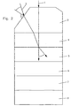
- This angle is achieved according to the invention by connecting a specially designed multilayer: For this purpose, a modified retroreflector in which the tip was cut off and the cut surface was polished was used (truncated pyramid). The beam guidance is shown in FIG. 2 .
- the light beams 1 , 2 are guided by the optical element 3 , which is designed as Einkoppel prism, via an immersion substance 4 of distilled water in the photoresist volume 5 , which is applied in this embodiment on a glass substrate 6 .
- a black anodized aluminum sheet as absorber 8 completes the beam path.
- substrate 6 and absorber 8 is another immersion substance 7 made of oil. Without these decoupling measures would be at the Underside of the substrate of the reference beam 1 partially and the other three beams 2 totally reflected and interfere with interference interference.
- the photoresist exposed to the interference pattern was heated to polymerization for about 6 minutes, with the temperature rising from about 65 ° C to about 92 ° C (post-exposure bake). After removal from the oven and cooling, the sample was allowed to rest for at least 30 minutes.
- the samples show cracks that occur due to the uneven volume change (swelling or shrinkage) during the development process. Sometimes the sample dissolves completely or partially from the substrate; Template are then also substrate-free. The area of the resulting fragments is about 1 mm 2 .
- the shape and size of the fragments can be controlled by targeted insertion of cracks in the photoresist (as predetermined breaking points).
- a targeted non-destructive detachment of the template from the substrate can be achieved by placing in a bath with heated or boiling hydrochloric acid.
- a further advantageous embodiment of the invention is the exposure of the photoresist through the glass substrate.
- the substrate 6, including the photoresist volume 5 applied thereto by means of spin coating is turned over. The irradiation occurs from the very flat side of the photoresist, which rests perfectly on the substrate 6 , rather than from the free, generally less perfect, facing away surface of the photoresist layer.
- All partial beams experience more or less strong reflection losses when entering from the outer medium (eg air) into the prism, which are avoided by providing all the entrance surfaces with antireflection layers suitable for the angle of incidence and the respective polarization.
- the outer medium eg air
- the inclined entrance surfaces are oriented such that the rays produce the desired one, especially at normal entry into the side surfaces of the prism Give angles in the photoresist.
- the residual reflection also present in the case of antireflection coating
- the reflection of a beam in itself is particularly easy to verify.
- an antireflection coating results irrespective of the beam polarization.
- the immersion substance and the material of which the prism is made are selected so that they have the same refractive index as the photoresist. This also low back reflections are avoided and increases the coupling efficiency.
- the lateral entry surfaces are just oriented so that they with correct adjustment with respect to the incoming rays are below the Brewster angle.
- the correct setting of the angle can be detected very precisely as the disappearance of the reflection of the p-portion of the beam.
- all four beams are set up parallel to each other, but they are laterally offset from each other.
- the entrance faces of the prism are oriented to give the required angles by refraction upon entry into the prism.
- the required parallelism of the beams can be realized with high accuracy, for example by means of beam splitters made of plane-parallel plates of suitable thickness. The task of precise angle adjustment between the four beams is thus almost completely transferred to the very well-controlled production of calculated angles in prism production.
- another prism which may be identical to the prism used for the coupling, is used for coupling out those light beams which have already passed through the photoresist and the substrate.
- the decoupled beams are then available for further analysis, for example for the control of the polarization states of the beams.
- a further advantageous embodiment of the beam configuration consists in dividing the laser beam into four partial beams, the wave vectors of two beams lying in one plane and the wave vectors of the two other beams in a further plane perpendicular to the first plane.
- the wave pair whose wave vectors lie in the first plane propagates counter to the wave pair in the other plane ( KI Petsas et al., PRA 1994, 50, page 5173 ).
- the bisector between two partial beams is common to both pairs and at the same time forms the solder to the photoresist layer.
- the photoresist layer is exposed from two sides, ie, two half-spaces separated by the photoresist layer.
- areas of the photoresist are specifically masked during the exposure, so that only parts of the interference pattern are preserved in the photoresist. This gives, for example, template selectable edge shape. This procedure is of interest for both positive and negative photoresists, because the unexposed parts, ie the parts covered by the mask, either stop or become dissolved.
- the photoresist can be overexposed in certain areas in certain embodiments. Thereafter, the multi-beam interference technique described above is also applied to the still unexposed portions. With a negative photoresist, the overexposed areas form solid material. The result is a photo-resist template, which is surrounded by solid material. This allows for better handling of the resulting photoresist template, especially when the entire photoresist layer is peeled from the substrate. By changing to positive photoresist complementary structures can be realized.
- a further photoresist layer for example, also from SU-8, which then with an interference pattern is exposed.
- a template is obtained which, after detachment from the substrate, lies on a solid material layer of photoresist (adhesive layer).
- This adhesive layer then forms a substrate of small thickness, which has the same chemical composition as the photoresist structure.
- the absorption of the light during propagation through the photoresist there is a decrease in the light intensity along the direction of propagation and thus, in a further embodiment, the possibility of a variation of the filling factor with the depth (gradient structure).
- the absorption and thus the strength of the variation can be influenced with the depth.
- the effective beam cross section is different than that of the original, for example, round beam.
- a better overlap of all beams is achieved by preforming them with known optical elements such as anamorphic prism pairs in their cross-section so that they effectively become circular by the oblique incidence.
- a special embodiment of the method according to the invention consists in using only three beams. As a result, two-dimensional periodic photoresist structures can be produced. With the aid of a coupling prism according to the invention, larger angles between the beams in the photoresist volume can be realized and thus smaller lattice constants than with direct irradiation from air.
Landscapes
- Physics & Mathematics (AREA)
- Engineering & Computer Science (AREA)
- Nanotechnology (AREA)
- General Physics & Mathematics (AREA)
- Optics & Photonics (AREA)
- Chemical & Material Sciences (AREA)
- Microelectronics & Electronic Packaging (AREA)
- Crystallography & Structural Chemistry (AREA)
- Life Sciences & Earth Sciences (AREA)
- Biophysics (AREA)
- Exposure And Positioning Against Photoresist Photosensitive Materials (AREA)
- Exposure Of Semiconductors, Excluding Electron Or Ion Beam Exposure (AREA)
- Light Receiving Elements (AREA)
- Steroid Compounds (AREA)
- Optical Communication System (AREA)
- Diffracting Gratings Or Hologram Optical Elements (AREA)
- Holo Graphy (AREA)
- Application Of Or Painting With Fluid Materials (AREA)
Claims (15)
- Procédé de production de structures de laque photosensible, dans lequel un volume en laque photosensible (5) est éclairé au moins une fois avec au moins trois faisceaux lumineux qui se superposent à l'intérieur du volume en laque photosensible (5) et est ensuite soumis à un processus de développement, les faisceaux lumineux traversant au moins un élément optique transparent (3) et l'élément optique (3) étant un polyèdre avec des surfaces planes ou courbées.
- Procédé de production de structures en laque photosensible selon la revendication 1,
caractérisé en ce qu'
il est prévu au moins deux éclairages du volume en laque photosensible (5), entre lesquels les faisceaux lumineux et le volume en laque photosensible (5) se déplacent relativement l'un à l'autre. - Procédé de production de structures en laque photosensible, selon lequel un volume en laque photosensible (5) est éclairé au moins deux fois avec au moins deux faisceaux lumineux (1, 2) qui se superposent à l'intérieur du volume en laque photosensible (5), les faisceaux lumineux (1, 2) et le volume en laque photosensible (5) se déplaçant relativement l'un à l'autre entre les au moins deux éclairages du volume en laque photosensible (5), et est ensuite soumis à un processus de développement, les faisceaux lumineux (1, 2) traversant au moins un élément optique transparent (3) et l'élément optique (3) étant un polyèdre avec des surfaces planes ou courbées.
- Procédé de production de structures en laque photosensible selon l'une des revendications 1 à 3,
caractérisé en ce qu'
un prisme partiel avec surfaces planes est utilisé comme polyèdre. - Procédé de production de structures en laque photosensible selon la revendication 4,
caractérisé en ce qu'
une pyramide est utilisée comme prisme partiel. - Procédé de production de structures en laque photosensible selon la revendication 4,
caractérisé en ce qu'
une pyramide tronquée est utilisée comme prisme partiel. - Procédé de production de structures en laque photosensible selon l'une des revendications 1 à 3,
caractérisé en ce qu'
un segment sphérique est utilisé comme prisme partiel. - Procédé de production de structures en laque photosensible selon l'une des revendications 1 à 7,
caractérisé en ce que
le volume en laque photosensible (5) est appliqué directement sur l'un des éléments optiques (3). - Procédé de production de structures en laque photosensible selon l'une des revendications 1 à 8,
caractérisé en ce qu'
on utilise deux éléments optiques entre lesquels se trouve le volume en laque photosensible (5). - Procédé de production de structures en laque photosensible selon l'une des revendications 1 à 9,
caractérisé par
une substance d'immersion (4) placée entre au moins un des éléments optiques (3) et le volume en laque photosensible (5). - Procédé de production de structures en laque photosensible selon l'une des revendications 1 à 10,
caractérisé en ce que
les faisceaux lumineux (1, 2) sont agencés indépendamment les uns des autres en ce qui concerne leur intensité, leur phase et leur polarisation. - Procédé de production de structures en laque photosensible selon l'une des revendications 1 à 11,
caractérisé en ce que
certaines zones de la surface du volume en laque photosensible (5) sont recouvertes d'au moins un masque d'ombre. - Procédé de production de structures en laque photosensible selon l'une des revendications 1 à 12,
caractérisé en ce que
le volume en laque photosensible (5) est éclairé en outre avec un faisceau individuel. - Procédé de production de structures en laque photosensible selon l'une des revendications 1 à 13,
caractérisé en ce que
le volume en laque photosensible (5) est décomposé en segments. - Procédé de production de structures en laque photosensible selon l'une des revendications 1 à 14,
caractérisé en ce que
le volume en laque photosensible est appliqué sur un autre volume en laque photosensible éclairé avec au moins un faisceau.
Applications Claiming Priority (3)
| Application Number | Priority Date | Filing Date | Title |
|---|---|---|---|
| DE10233309 | 2002-07-22 | ||
| DE10233309 | 2002-07-22 | ||
| PCT/EP2003/007819 WO2004010222A2 (fr) | 2002-07-22 | 2003-07-18 | Procede de production de structure de laque photosensible |
Publications (2)
| Publication Number | Publication Date |
|---|---|
| EP1523697A2 EP1523697A2 (fr) | 2005-04-20 |
| EP1523697B1 true EP1523697B1 (fr) | 2007-12-05 |
Family
ID=30469035
Family Applications (1)
| Application Number | Title | Priority Date | Filing Date |
|---|---|---|---|
| EP03765041A Expired - Lifetime EP1523697B1 (fr) | 2002-07-22 | 2003-07-18 | Procede de production de structure de laque photosensible |
Country Status (6)
| Country | Link |
|---|---|
| US (1) | US7407737B2 (fr) |
| EP (1) | EP1523697B1 (fr) |
| JP (1) | JP2005534050A (fr) |
| AT (1) | ATE380359T1 (fr) |
| DE (2) | DE50308738D1 (fr) |
| WO (1) | WO2004010222A2 (fr) |
Families Citing this family (6)
| Publication number | Priority date | Publication date | Assignee | Title |
|---|---|---|---|---|
| US7492442B2 (en) * | 2004-08-27 | 2009-02-17 | Asml Holding N.V. | Adjustable resolution interferometric lithography system |
| DE102005025207B4 (de) * | 2005-05-25 | 2015-07-23 | E.G.O. Elektro-Gerätebau GmbH | Wärmedämmung für eine Strahlungsheizeinrichtung, Strahlungsheizeinrichtung und Elektro-Haushaltsgerät |
| US7708924B2 (en) * | 2005-07-21 | 2010-05-04 | Asml Netherlands B.V. | Imprint lithography |
| US7692771B2 (en) * | 2005-05-27 | 2010-04-06 | Asml Netherlands B.V. | Imprint lithography |
| WO2014201414A1 (fr) * | 2013-06-14 | 2014-12-18 | The Trustees Of Dartmouth College | Procédés de fabrication de dispositifs magnétiques et systèmes et dispositifs associés |
| US10345705B2 (en) | 2013-07-12 | 2019-07-09 | Xerox Corporation | Photolithographic patterning of a cylinder |
Family Cites Families (12)
| Publication number | Priority date | Publication date | Assignee | Title |
|---|---|---|---|---|
| GB1267858A (en) * | 1968-09-19 | 1972-03-22 | Agfa Gevaert Ag | Holographic process |
| GB1289095A (fr) * | 1968-10-02 | 1972-09-13 | ||
| DE2224350C3 (de) * | 1972-05-18 | 1975-01-09 | Siemens Ag, 1000 Berlin Und 8000 Muenchen | Anordnung zum Auslesen von holografisch gespeicherten Informationen |
| JPS61190368A (ja) * | 1985-02-20 | 1986-08-25 | Matsushita Electric Ind Co Ltd | 微細パタ−ンの形成方法 |
| US5017263A (en) * | 1988-12-23 | 1991-05-21 | At&T Bell Laboratories | Optoelectronic device package method |
| GB8922341D0 (en) | 1989-10-04 | 1989-11-22 | Holtronic Technologies Ltd | Apparatus for and method of optical inspection in a total internal reflection holographic imaging system |
| US5461455A (en) * | 1993-08-23 | 1995-10-24 | International Business Machines Corporation | Optical system for the projection of patterned light onto the surfaces of three dimensional objects |
| GB2311144B (en) | 1996-03-12 | 2000-05-24 | Holtronic Technologies Ltd | Method and apparatus for holographically recording an essentially periodic pattern |
| JPH11248913A (ja) * | 1998-03-03 | 1999-09-17 | Nikon Corp | 狭帯化素子 |
| EP1192509A1 (fr) | 1999-06-11 | 2002-04-03 | Holtronic Technologies Plc | Procede et dispositif d'enregistrement d'un hologramme a partir d'un motif de masque et au moyen d'une holographie par reflexion totale et interieure, et hologramme fabrique selon ce procede |
| GB9922196D0 (en) | 1999-09-20 | 1999-11-17 | Isis Innovation | Photonic crystal materials |
| GB2372107A (en) | 2001-02-08 | 2002-08-14 | Holtronic Technologies Plc | Reconstructing an image from a total internal reflection hologram |
-
2003
- 2003-07-18 JP JP2004522501A patent/JP2005534050A/ja active Pending
- 2003-07-18 AT AT03765041T patent/ATE380359T1/de not_active IP Right Cessation
- 2003-07-18 EP EP03765041A patent/EP1523697B1/fr not_active Expired - Lifetime
- 2003-07-18 US US10/522,162 patent/US7407737B2/en not_active Expired - Fee Related
- 2003-07-18 WO PCT/EP2003/007819 patent/WO2004010222A2/fr not_active Ceased
- 2003-07-18 DE DE50308738T patent/DE50308738D1/de not_active Expired - Lifetime
- 2003-07-18 DE DE10332651A patent/DE10332651A1/de not_active Ceased
Also Published As
| Publication number | Publication date |
|---|---|
| JP2005534050A (ja) | 2005-11-10 |
| US7407737B2 (en) | 2008-08-05 |
| DE10332651A1 (de) | 2004-02-26 |
| WO2004010222A2 (fr) | 2004-01-29 |
| EP1523697A2 (fr) | 2005-04-20 |
| DE50308738D1 (de) | 2008-01-17 |
| ATE380359T1 (de) | 2007-12-15 |
| WO2004010222A3 (fr) | 2004-10-14 |
| US20060154178A1 (en) | 2006-07-13 |
Similar Documents
| Publication | Publication Date | Title |
|---|---|---|
| DE60301297T2 (de) | Polarisierendes optisches Element und Herstellungsverfahren dafür | |
| DE69227332T2 (de) | Nichtlinearoptisches Element und seine Verwendung | |
| DE60004146T2 (de) | Methode und Anordnung zur Herstellung eines photonischen Kristalls | |
| DE69819013T2 (de) | Photonen-kristall und seine herstellungsmethode | |
| DE69303320T2 (de) | Herstellung von Mikrostrukturen unterschiedlicher Strukturhöhe mittels Röntgentiefenlithographie mit Opfermetallschicht | |
| DE69923292T2 (de) | Omnidirektionaler reflektor aus photonischem kristall | |
| WO2005017620A2 (fr) | Dispositif d'eclairage et polariseur destines a un systeme d'exposition de projection microlithographique | |
| DE10344010A1 (de) | Wabenkondensor und Beleuchtungssystem damit | |
| DE102018003675A1 (de) | Verfahren zum Abtrennen von Festkörperschichten von Kompositstrukturen aus SiC und einer metallischen Beschichtung oder elektrischen Bauteilen | |
| DE112012003512B4 (de) | Verfahren zum Trennen einer Schicht von einer Verbundstruktur | |
| DE10311809A1 (de) | Polarisationsoptimiertes Beleuchtungssystem | |
| DE3019851A1 (de) | Verfahren zur herstellung einer lithographie-maske und mit einem solchen verfahren hergestellte maske | |
| EP1523697B1 (fr) | Procede de production de structure de laque photosensible | |
| DE102021123801A1 (de) | Verfahren und Vorrichtung zur Laserbearbeitung eines Werkstücks | |
| DE3524176A1 (de) | Lichtmaske und verfahren fuer ihre herstellung | |
| EP3077858B1 (fr) | Système de polarisation | |
| DE112006001230B4 (de) | Bearbeitungsverfahren und Bearbeitungsvorrichtung, die interferierende Laserstrahlen verwenden, sowie Beugungsgitter und Miktrostruktur, hergestellt mit dem Barbeiungsverfahren | |
| DE102020133528B3 (de) | Verfahren zur Herstellung einer optischen Komponente mit innerer, beschichteter Struktur und danach hergestellte optische Komponente | |
| WO2004102273A2 (fr) | Systeme d'eclairage pourvu d'un module axicon | |
| DE69315484T2 (de) | Polarisationsempfindlicher Strahlteiler, Methode zur Herstellung eines solchen und magneto-optische Abtastvorrichtung mit einem solchen Strahlteiler | |
| DE102021117204A1 (de) | Vorrichtung und Verfahren zur Laserinterferenzstrukturierung von transparenten Substraten mit periodischen Punktstrukturen für Antireflexionseigenschaften | |
| DE10017614B4 (de) | Verfahren zur Herstellung einer dielektrischen Reflexionsmaske | |
| DE69325192T2 (de) | Verfahren zur Formung und Denaturierung von Partikeln | |
| DE10312003B4 (de) | Verfahren zur Herstellung eines transmissiven doppelbrechend wirkenden optischen Elements sowie transmissives doppelbrechend wirkendes optisches Element | |
| DE102012109130B4 (de) | Verfahren und Vorrichtungen zur Herstellung dreidimensionaler Strukturen |
Legal Events
| Date | Code | Title | Description |
|---|---|---|---|
| PUAI | Public reference made under article 153(3) epc to a published international application that has entered the european phase |
Free format text: ORIGINAL CODE: 0009012 |
|
| 17P | Request for examination filed |
Effective date: 20041104 |
|
| AK | Designated contracting states |
Kind code of ref document: A2 Designated state(s): AT BE BG CH CY CZ DE DK EE ES FI FR GB GR HU IE IT LI LU MC NL PT RO SE SI SK TR |
|
| GRAP | Despatch of communication of intention to grant a patent |
Free format text: ORIGINAL CODE: EPIDOSNIGR1 |
|
| GRAS | Grant fee paid |
Free format text: ORIGINAL CODE: EPIDOSNIGR3 |
|
| GRAA | (expected) grant |
Free format text: ORIGINAL CODE: 0009210 |
|
| AK | Designated contracting states |
Kind code of ref document: B1 Designated state(s): AT BE BG CH CY CZ DE DK EE ES FI FR GB GR HU IE IT LI LU MC NL PT RO SE SI SK TR |
|
| REG | Reference to a national code |
Ref country code: GB Ref legal event code: FG4D Free format text: NOT ENGLISH |
|
| REG | Reference to a national code |
Ref country code: IE Ref legal event code: FG4D Free format text: LANGUAGE OF EP DOCUMENT: GERMAN |
|
| REG | Reference to a national code |
Ref country code: CH Ref legal event code: EP |
|
| REG | Reference to a national code |
Ref country code: CH Ref legal event code: NV Representative=s name: ROTTMANN, ZIMMERMANN + PARTNER AG |
|
| REF | Corresponds to: |
Ref document number: 50308738 Country of ref document: DE Date of ref document: 20080117 Kind code of ref document: P |
|
| PG25 | Lapsed in a contracting state [announced via postgrant information from national office to epo] |
Ref country code: ES Free format text: LAPSE BECAUSE OF FAILURE TO SUBMIT A TRANSLATION OF THE DESCRIPTION OR TO PAY THE FEE WITHIN THE PRESCRIBED TIME-LIMIT Effective date: 20080316 Ref country code: SE Free format text: LAPSE BECAUSE OF FAILURE TO SUBMIT A TRANSLATION OF THE DESCRIPTION OR TO PAY THE FEE WITHIN THE PRESCRIBED TIME-LIMIT Effective date: 20080305 |
|
| PG25 | Lapsed in a contracting state [announced via postgrant information from national office to epo] |
Ref country code: FI Free format text: LAPSE BECAUSE OF FAILURE TO SUBMIT A TRANSLATION OF THE DESCRIPTION OR TO PAY THE FEE WITHIN THE PRESCRIBED TIME-LIMIT Effective date: 20071205 Ref country code: SI Free format text: LAPSE BECAUSE OF FAILURE TO SUBMIT A TRANSLATION OF THE DESCRIPTION OR TO PAY THE FEE WITHIN THE PRESCRIBED TIME-LIMIT Effective date: 20071205 |
|
| PG25 | Lapsed in a contracting state [announced via postgrant information from national office to epo] |
Ref country code: CZ Free format text: LAPSE BECAUSE OF FAILURE TO SUBMIT A TRANSLATION OF THE DESCRIPTION OR TO PAY THE FEE WITHIN THE PRESCRIBED TIME-LIMIT Effective date: 20071205 |
|
| ET | Fr: translation filed | ||
| PG25 | Lapsed in a contracting state [announced via postgrant information from national office to epo] |
Ref country code: SK Free format text: LAPSE BECAUSE OF FAILURE TO SUBMIT A TRANSLATION OF THE DESCRIPTION OR TO PAY THE FEE WITHIN THE PRESCRIBED TIME-LIMIT Effective date: 20071205 Ref country code: RO Free format text: LAPSE BECAUSE OF FAILURE TO SUBMIT A TRANSLATION OF THE DESCRIPTION OR TO PAY THE FEE WITHIN THE PRESCRIBED TIME-LIMIT Effective date: 20071205 |
|
| PG25 | Lapsed in a contracting state [announced via postgrant information from national office to epo] |
Ref country code: PT Free format text: LAPSE BECAUSE OF FAILURE TO SUBMIT A TRANSLATION OF THE DESCRIPTION OR TO PAY THE FEE WITHIN THE PRESCRIBED TIME-LIMIT Effective date: 20080505 |
|
| REG | Reference to a national code |
Ref country code: IE Ref legal event code: FD4D |
|
| PLBE | No opposition filed within time limit |
Free format text: ORIGINAL CODE: 0009261 |
|
| STAA | Information on the status of an ep patent application or granted ep patent |
Free format text: STATUS: NO OPPOSITION FILED WITHIN TIME LIMIT |
|
| PG25 | Lapsed in a contracting state [announced via postgrant information from national office to epo] |
Ref country code: DK Free format text: LAPSE BECAUSE OF FAILURE TO SUBMIT A TRANSLATION OF THE DESCRIPTION OR TO PAY THE FEE WITHIN THE PRESCRIBED TIME-LIMIT Effective date: 20071205 Ref country code: IE Free format text: LAPSE BECAUSE OF FAILURE TO SUBMIT A TRANSLATION OF THE DESCRIPTION OR TO PAY THE FEE WITHIN THE PRESCRIBED TIME-LIMIT Effective date: 20071205 |
|
| 26N | No opposition filed |
Effective date: 20080908 |
|
| PG25 | Lapsed in a contracting state [announced via postgrant information from national office to epo] |
Ref country code: GR Free format text: LAPSE BECAUSE OF FAILURE TO SUBMIT A TRANSLATION OF THE DESCRIPTION OR TO PAY THE FEE WITHIN THE PRESCRIBED TIME-LIMIT Effective date: 20080306 |
|
| PG25 | Lapsed in a contracting state [announced via postgrant information from national office to epo] |
Ref country code: MC Free format text: LAPSE BECAUSE OF NON-PAYMENT OF DUE FEES Effective date: 20080731 |
|
| PG25 | Lapsed in a contracting state [announced via postgrant information from national office to epo] |
Ref country code: EE Free format text: LAPSE BECAUSE OF FAILURE TO SUBMIT A TRANSLATION OF THE DESCRIPTION OR TO PAY THE FEE WITHIN THE PRESCRIBED TIME-LIMIT Effective date: 20071205 Ref country code: BG Free format text: LAPSE BECAUSE OF FAILURE TO SUBMIT A TRANSLATION OF THE DESCRIPTION OR TO PAY THE FEE WITHIN THE PRESCRIBED TIME-LIMIT Effective date: 20080305 |
|
| PG25 | Lapsed in a contracting state [announced via postgrant information from national office to epo] |
Ref country code: CY Free format text: LAPSE BECAUSE OF FAILURE TO SUBMIT A TRANSLATION OF THE DESCRIPTION OR TO PAY THE FEE WITHIN THE PRESCRIBED TIME-LIMIT Effective date: 20071205 |
|
| PG25 | Lapsed in a contracting state [announced via postgrant information from national office to epo] |
Ref country code: HU Free format text: LAPSE BECAUSE OF FAILURE TO SUBMIT A TRANSLATION OF THE DESCRIPTION OR TO PAY THE FEE WITHIN THE PRESCRIBED TIME-LIMIT Effective date: 20080606 Ref country code: LU Free format text: LAPSE BECAUSE OF NON-PAYMENT OF DUE FEES Effective date: 20080718 |
|
| PG25 | Lapsed in a contracting state [announced via postgrant information from national office to epo] |
Ref country code: TR Free format text: LAPSE BECAUSE OF FAILURE TO SUBMIT A TRANSLATION OF THE DESCRIPTION OR TO PAY THE FEE WITHIN THE PRESCRIBED TIME-LIMIT Effective date: 20071205 |
|
| PGFP | Annual fee paid to national office [announced via postgrant information from national office to epo] |
Ref country code: CH Payment date: 20100726 Year of fee payment: 8 Ref country code: NL Payment date: 20100726 Year of fee payment: 8 |
|
| PGFP | Annual fee paid to national office [announced via postgrant information from national office to epo] |
Ref country code: AT Payment date: 20100721 Year of fee payment: 8 |
|
| PG25 | Lapsed in a contracting state [announced via postgrant information from national office to epo] |
Ref country code: IT Free format text: LAPSE BECAUSE OF NON-PAYMENT OF DUE FEES Effective date: 20080731 |
|
| PGFP | Annual fee paid to national office [announced via postgrant information from national office to epo] |
Ref country code: BE Payment date: 20100726 Year of fee payment: 8 |
|
| REG | Reference to a national code |
Ref country code: CH Ref legal event code: PFA Owner name: FORSCHUNGSZENTRUM KARLSRUHE GMBH Free format text: FORSCHUNGSZENTRUM KARLSRUHE GMBH#WEBERSTRASSE 5#76133 KARLSRUHE (DE) -TRANSFER TO- FORSCHUNGSZENTRUM KARLSRUHE GMBH#WEBERSTRASSE 5#76133 KARLSRUHE (DE) |
|
| BERE | Be: lapsed |
Owner name: FORSCHUNGSZENTRUM KARLSRUHE G.M.B.H. Effective date: 20110731 |
|
| REG | Reference to a national code |
Ref country code: NL Ref legal event code: V1 Effective date: 20120201 |
|
| REG | Reference to a national code |
Ref country code: CH Ref legal event code: PL |
|
| REG | Reference to a national code |
Ref country code: AT Ref legal event code: MM01 Ref document number: 380359 Country of ref document: AT Kind code of ref document: T Effective date: 20110718 |
|
| PG25 | Lapsed in a contracting state [announced via postgrant information from national office to epo] |
Ref country code: CH Free format text: LAPSE BECAUSE OF NON-PAYMENT OF DUE FEES Effective date: 20110731 Ref country code: LI Free format text: LAPSE BECAUSE OF NON-PAYMENT OF DUE FEES Effective date: 20110731 Ref country code: BE Free format text: LAPSE BECAUSE OF NON-PAYMENT OF DUE FEES Effective date: 20110731 |
|
| PG25 | Lapsed in a contracting state [announced via postgrant information from national office to epo] |
Ref country code: NL Free format text: LAPSE BECAUSE OF NON-PAYMENT OF DUE FEES Effective date: 20120201 |
|
| PGFP | Annual fee paid to national office [announced via postgrant information from national office to epo] |
Ref country code: GB Payment date: 20120723 Year of fee payment: 10 |
|
| PGFP | Annual fee paid to national office [announced via postgrant information from national office to epo] |
Ref country code: DE Payment date: 20120921 Year of fee payment: 10 Ref country code: FR Payment date: 20120803 Year of fee payment: 10 |
|
| PG25 | Lapsed in a contracting state [announced via postgrant information from national office to epo] |
Ref country code: AT Free format text: LAPSE BECAUSE OF NON-PAYMENT OF DUE FEES Effective date: 20110718 |
|
| GBPC | Gb: european patent ceased through non-payment of renewal fee |
Effective date: 20130718 |
|
| REG | Reference to a national code |
Ref country code: DE Ref legal event code: R119 Ref document number: 50308738 Country of ref document: DE Effective date: 20140201 |
|
| REG | Reference to a national code |
Ref country code: FR Ref legal event code: ST Effective date: 20140331 |
|
| PG25 | Lapsed in a contracting state [announced via postgrant information from national office to epo] |
Ref country code: GB Free format text: LAPSE BECAUSE OF NON-PAYMENT OF DUE FEES Effective date: 20130718 Ref country code: DE Free format text: LAPSE BECAUSE OF NON-PAYMENT OF DUE FEES Effective date: 20140201 |
|
| PG25 | Lapsed in a contracting state [announced via postgrant information from national office to epo] |
Ref country code: FR Free format text: LAPSE BECAUSE OF NON-PAYMENT OF DUE FEES Effective date: 20130731 |