EP1523185A1 - Image data conversion method, conversion circuit, and digital camera - Google Patents
Image data conversion method, conversion circuit, and digital camera Download PDFInfo
- Publication number
- EP1523185A1 EP1523185A1 EP04726301A EP04726301A EP1523185A1 EP 1523185 A1 EP1523185 A1 EP 1523185A1 EP 04726301 A EP04726301 A EP 04726301A EP 04726301 A EP04726301 A EP 04726301A EP 1523185 A1 EP1523185 A1 EP 1523185A1
- Authority
- EP
- European Patent Office
- Prior art keywords
- image data
- format
- field
- circuit
- frame
- Prior art date
- Legal status (The legal status is an assumption and is not a legal conclusion. Google has not performed a legal analysis and makes no representation as to the accuracy of the status listed.)
- Granted
Links
Images






Classifications
-
- H—ELECTRICITY
- H04—ELECTRIC COMMUNICATION TECHNIQUE
- H04N—PICTORIAL COMMUNICATION, e.g. TELEVISION
- H04N7/00—Television systems
- H04N7/01—Conversion of standards, e.g. involving analogue television standards or digital television standards processed at pixel level
-
- H—ELECTRICITY
- H04—ELECTRIC COMMUNICATION TECHNIQUE
- H04N—PICTORIAL COMMUNICATION, e.g. TELEVISION
- H04N7/00—Television systems
- H04N7/01—Conversion of standards, e.g. involving analogue television standards or digital television standards processed at pixel level
- H04N7/0135—Conversion of standards, e.g. involving analogue television standards or digital television standards processed at pixel level involving interpolation processes
Definitions
- Each frame of image data is retrieved from, for example, a CCD image sensor or a recording medium every 1/30 seconds, and is converted into that in the PAL format.
- image data in the PAL format can be obtained by decimating one frame in the NTSC format every six frames, thereby enabling an easy frame conversion.
- the present invention is intended to solve the above problems.
- the method includes the steps of: retrieving respective signals required for producing image data of an odd field and an even field in the second format, out of moving image data in the first format from a memory to which the moving image data in the first format is written, every odd field period and every even field period in the second format, respectively; converting the retrieved image data into first image data and second image data, both image data having the second line frequency; outputting the image data of the odd field in the second format by mixing image data of an odd field of the first image data and image data of an odd field of the second image data at a predetermined mixing ratio; outputting the image data of the even field in the second format by mixing image data of an even field of the first image data and image data of an even field of the second image data at a predetermined mixing ratio; and changing the mixing ratios every field period in the second format.
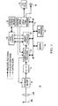
- the image data is supplied to a camera signal-processing circuit 13, and is converted to image data in the Y-signal, U-signal, and V-signal (YUV) format after processes, for example, white balance correction and gamma correction.
- the converted image data is written to an area for display in a memory 16 by a memory controller 14 through an image bus 15.
- the area for display in the memory 16 functions as a so-called video random access memory (RAM). Addresses of the area respectively correspond to dot positions on a display screen.
- RAM video random access memory
- the CCD image sensor 11 when moving images are captured, the CCD image sensor 11 is controlled so as to capture an image in the NTSC format and to output image data, i.e., original image data once every frame period.
- image data i.e., original image data once every frame period.
- fields of two continuous frames of the original image data are mixed at a predetermined ratio that changes every field period to form the output image data (the output video signals).
- both the frame frequency and the line frequency of the original image data are different from those of the output image data.
- both frame conversion and line conversion are carried out.
- lines of the original image data are converted, and frames of this image data after line conversion are then converted to obtain the output image data.
- image data having 576 effective lines in the PAL format can be generated from the original image data having 480 effective lines by interpolating image data of an intermediate line between two continuous lines of the original image data.
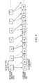
- This frame conversion converts the image data after line conversion according to expression (2) into output image data in the PAL format by interpolation, as shown in parts A and B of Fig. 4.
- Part A of Fig. 4 shows the image data after line conversion according to expression (2) in units of frames
- part B of Fig. 4 shows the output image data after frame conversion in units of frames.
- the microcomputer 22 supplies the odd-field start address A_STAD and a clock CK to the register 141, which stores the start address A__STAD.
- An output from the register 141 and the pulses NTFRM from the signal-generating circuit 171 are supplied to the register 142, which stores the odd-field start address A_STAD.
- An output from the register 142 and the pulses FLDPLS from the signal-generating circuit 172 are supplied to the register 143, which outputs the odd-field start address A_STAD every pulse FLDPLS.
- the odd-field start address A_STAD, the even-field start address B_STAD, and the signals FLDRCT serving as control signals output from the signal-generating circuit 172 are supplied to a data selector 148 (in this case, the signals FLDRCT invert every PAL field period).
- the data selector 148 alternately outputs the odd-field start address A_STAD and the even-field start address B_STAD every PAL field period.
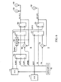
- These synchronized image data d m and d m+1 are supplied to the subtracting circuit 732, which subtracts the data d m from the data d m+1 and supplies the result (d m+1 - d m ) to the multiplying circuit 733.
- the coefficient KL is also supplied to the multiplying circuit 733 from a coefficient-generating circuit 76, described below, to be multiplied by the value (d m+1 - d m ).
- the result KL (d m+1 - d m ) and the data d m from the converting circuit 731 are supplied to the adding circuit 734.
- This image data dOUT is used as image data D n of the n-th frame in expression (1), and is hereinafter replaced by image data D n (after line conversion).
- This image data DOUT is D/A-converted to analog color video signals to be output to the external video output terminal 19.
- images are displayed, in the PAL format, on a monitoring television receiver connected to the - external video output terminal 19.
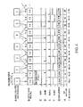
- the output QL from the register 763 is set to the initial value A_OFF or the initial value B_OFF at the start point of every field period of the output image data. Subsequently, the output QL changes to the value obtained by adding the delta value LPHASE to the initial value every horizontal line period, as shown in Fig. 3.
- the output QL is supplied as the coefficient KL to the multiplying circuit 733 in the line-interpolating circuit 73 and the multiplying circuit 743 in the line-interpolating circuit 74, where line conversion is carried out.
Landscapes
- Engineering & Computer Science (AREA)
- Multimedia (AREA)
- Signal Processing (AREA)
- Television Systems (AREA)
- Studio Devices (AREA)
Abstract
Description
Claims (8)
- A method for converting image data in a first format into image data in a second format, the image data in the first format having a first frame frequency and a first line frequency, the image data in the second format having a second frame frequency and a second line frequency, the method comprising the steps of:retrieving respective signals required for producing image data of an odd field and an even field in the second format, out of moving image data in the first format from a memory to which the moving image data in the first format is written, every odd field period and every even field period in the second format, respectively;converting the retrieved image data into first image data and second image data, both image data having the second line frequency;outputting the image data of the odd field in the second format by mixing image data of an odd field of the first image data and image data of an odd field of the second image data at a predetermined mixing ratio;outputting the image data of the even field in the second format by mixing image data of an even field of the first image data and image data of an even field of the second image data at a predetermined mixing ratio; andchanging the mixing ratios every field period in the second format.
- The method for converting image data according to claim 1, whereinthe first format is the National Television System Committee (NTSC) format; andthe second format is the Phase Alternation by Line (PAL) format.
- The method for converting image data according to claim 1, whereinthe first format is the NTSC format; andthe second format is switched to the NTSC format or the PAL format.
- A converting circuit for converting image data in a first format into image data in a second format, the image data in the first format having a first frame frequency and a first line frequency, the image data in the second format having a second frame frequency and a second line frequency, the converting circuit comprising:a memory to which moving image data in the first format is written;a first circuit retrieving respective signals required for producing image data of an odd field and an even field in the second format, out of the moving image data in the first format from the memory, every odd field period and every even field period in the second format, respectively;a second circuit converting the retrieved image data into first image data and second image data, both image data having the second line frequency;a third circuit outputting the image data of the odd field in the second format by mixing image data of an odd field of the first image data and image data of an odd field of the second image data at a predetermined mixing ratio, and outputting the image data of the even field in the second format by mixing image data of an even field of the first image data and image data of an even field of the second image data at a predetermined mixing ratio; anda fourth circuit changing the mixing ratios every field period in the second format.
- The frame-converting circuit according to claim 4, whereinthe first format is the NTSC format; andthe second format is the PAL format.
- The frame-converting circuit according to claim 4, further comprising:a circuit in which the second format is switched to the NTSC format or the PAL format, whereinthe first format is the NTSC format.
- An electronic camera wherein image data in a first format has a first frame frequency and a first line frequency and image data in a second format has a second frame frequency and a second line frequency, the electronic camera comprising:an image sensor, onto which an image of an object is projected, outputting the image data in the first format every frame period of the first format;a memory to which the image data in the first format output from the image sensor is written;a first circuit retrieving respective signals required for producing image data of an odd field and an even field in the second format, out of the image data in the first format from the memory, every odd field period and every even field period in the second format, respectively;a second circuit converting the retrieved image data into first image data and second image data, both image data having the second line frequency;a third circuit outputting the image data of the odd field in the second format by mixing image data of an odd field of the first image data and image data of an odd field of the second image data at a predetermined mixing ratio, and outputting the image data of the even field in the second format by mixing image data of an even field of the first image data and image data of an even field of the second image data at a predetermined mixing ratio;a fourth circuit changing the mixing ratios every field period in the second format; andan external terminal outputting the image data output from the third circuit.
- The electronic camera according to claim 7, further comprising:a circuit in which the second format is switched to the NTSC format or the PAL format, whereinthe first format is the NTSC format.
Applications Claiming Priority (3)
| Application Number | Priority Date | Filing Date | Title |
|---|---|---|---|
| JP2003132726 | 2003-05-12 | ||
| JP2003132726A JP3962928B2 (en) | 2003-05-12 | 2003-05-12 | Image data conversion method, conversion circuit, and imaging apparatus |
| PCT/JP2004/005028 WO2004100544A1 (en) | 2003-05-12 | 2004-04-07 | Image data conversion method, conversion circuit, and digital camera |
Publications (3)
| Publication Number | Publication Date |
|---|---|
| EP1523185A1 true EP1523185A1 (en) | 2005-04-13 |
| EP1523185A4 EP1523185A4 (en) | 2005-10-26 |
| EP1523185B1 EP1523185B1 (en) | 2018-06-06 |
Family
ID=33432174
Family Applications (1)
| Application Number | Title | Priority Date | Filing Date |
|---|---|---|---|
| EP04726301.7A Expired - Lifetime EP1523185B1 (en) | 2003-05-12 | 2004-04-07 | Image data conversion method, conversion circuit, and digital camera |
Country Status (7)
| Country | Link |
|---|---|
| US (1) | US7671913B2 (en) |
| EP (1) | EP1523185B1 (en) |
| JP (1) | JP3962928B2 (en) |
| KR (1) | KR101016490B1 (en) |
| CN (1) | CN100350796C (en) |
| TW (1) | TWI246331B (en) |
| WO (1) | WO2004100544A1 (en) |
Families Citing this family (12)
| Publication number | Priority date | Publication date | Assignee | Title |
|---|---|---|---|---|
| JP4178455B2 (en) * | 2003-01-21 | 2008-11-12 | ソニー株式会社 | Frame conversion method, frame conversion circuit, and electronic camera |
| WO2008015781A1 (en) * | 2006-08-01 | 2008-02-07 | Nikon Corporation | Image processing device and electronic camera |
| JP4312238B2 (en) * | 2007-02-13 | 2009-08-12 | 株式会社ソニー・コンピュータエンタテインメント | Image conversion apparatus and image conversion method |
| CN101399928B (en) * | 2007-09-29 | 2012-03-14 | 新奥特硅谷视频技术有限责任公司 | Non-linear editing system |
| CN101399945B (en) * | 2007-09-29 | 2012-03-14 | 新奥特硅谷视频技术有限责任公司 | Method for supporting NTSC system edition under PAL system environment |
| WO2011005413A2 (en) * | 2009-06-22 | 2011-01-13 | Omnivision Technologies, Inc. | System and method for an image sensor operable in multiple video standards |
| TW201108717A (en) * | 2009-08-17 | 2011-03-01 | Silicon Motion Inc | Image processing system and image processing method |
| JP5991495B2 (en) * | 2011-11-04 | 2016-09-14 | 株式会社ニコン | Image generating apparatus, imaging apparatus, and program |
| KR101427552B1 (en) * | 2014-03-31 | 2014-08-07 | (주) 넥스트칩 | Method and apparatus for transmitting video siganl |
| CN107222704B (en) * | 2017-06-21 | 2019-09-17 | 浙江大华技术股份有限公司 | A kind of video formats switching method and device |
| US11132296B1 (en) * | 2018-07-12 | 2021-09-28 | Xilinx, Inc. | Linear interpolator of tabulated functions |
| CN110248132B (en) * | 2019-05-31 | 2020-12-01 | 成都东方盛行电子有限责任公司 | Video frame rate interpolation method |
Family Cites Families (13)
| Publication number | Priority date | Publication date | Assignee | Title |
|---|---|---|---|---|
| JP2508419B2 (en) | 1985-08-08 | 1996-06-19 | ソニー株式会社 | Video signal frame frequency converter |
| JPS63156486A (en) * | 1986-12-20 | 1988-06-29 | Fujitsu General Ltd | Television signal conversion method |
| DE3838609A1 (en) * | 1988-11-15 | 1990-06-13 | Thomson Brandt Gmbh | IMAGE PROCESSING SYSTEM |
| JPH0478284A (en) | 1990-07-17 | 1992-03-12 | Victor Co Of Japan Ltd | Frame rate converter |
| KR940009970B1 (en) * | 1991-12-04 | 1994-10-19 | 삼성전자 주식회사 | Line conversion method of video signal and its device |
| KR0157566B1 (en) * | 1995-09-30 | 1998-11-16 | 김광호 | Interpolation method and device for high quality |
| JP2000165821A (en) * | 1998-11-30 | 2000-06-16 | Fujitsu Ltd | Image format conversion apparatus and image format conversion method |
| JP3998399B2 (en) * | 1999-12-03 | 2007-10-24 | 松下電器産業株式会社 | Video signal converter |
| JP2001313896A (en) | 2000-04-28 | 2001-11-09 | Sanyo Electric Co Ltd | Image-reproducing apparatus |
| US7012648B2 (en) * | 2001-04-02 | 2006-03-14 | Matsushita Electric Industrial Co., Ltd. | Image conversion method and image conversion apparatus |
| JP2002369155A (en) | 2001-04-02 | 2002-12-20 | Matsushita Electric Ind Co Ltd | Image conversion method and image conversion device |
| KR20040015965A (en) * | 2002-08-14 | 2004-02-21 | 엘지전자 주식회사 | Apparatus for conversing format |
| JP4178455B2 (en) * | 2003-01-21 | 2008-11-12 | ソニー株式会社 | Frame conversion method, frame conversion circuit, and electronic camera |
-
2003
- 2003-05-12 JP JP2003132726A patent/JP3962928B2/en not_active Expired - Fee Related
-
2004
- 2004-03-31 TW TW093108885A patent/TWI246331B/en not_active IP Right Cessation
- 2004-04-07 KR KR1020057000510A patent/KR101016490B1/en not_active Expired - Fee Related
- 2004-04-07 WO PCT/JP2004/005028 patent/WO2004100544A1/en not_active Ceased
- 2004-04-07 EP EP04726301.7A patent/EP1523185B1/en not_active Expired - Lifetime
- 2004-04-07 US US10/520,770 patent/US7671913B2/en not_active Expired - Fee Related
- 2004-04-07 CN CNB2004800004543A patent/CN100350796C/en not_active Expired - Fee Related
Also Published As
| Publication number | Publication date |
|---|---|
| CN100350796C (en) | 2007-11-21 |
| WO2004100544A1 (en) | 2004-11-18 |
| TWI246331B (en) | 2005-12-21 |
| JP3962928B2 (en) | 2007-08-22 |
| US7671913B2 (en) | 2010-03-02 |
| KR101016490B1 (en) | 2011-02-24 |
| EP1523185A4 (en) | 2005-10-26 |
| JP2004336608A (en) | 2004-11-25 |
| US20050237427A1 (en) | 2005-10-27 |
| TW200509697A (en) | 2005-03-01 |
| EP1523185B1 (en) | 2018-06-06 |
| CN1698372A (en) | 2005-11-16 |
| KR20060010705A (en) | 2006-02-02 |
Similar Documents
| Publication | Publication Date | Title |
|---|---|---|
| JP4424088B2 (en) | Imaging device | |
| JPH01319375A (en) | Imaging device | |
| US7671913B2 (en) | Method for converting image data, converting circuit for image, and electronic camera | |
| US6762792B1 (en) | Digital still camera | |
| JP2005244980A (en) | Apparatus and method for processing imaging signal | |
| US7236194B2 (en) | Image signal processing apparatus | |
| US7898595B2 (en) | Frame conversion method, frame conversion circuit, and electronic camera | |
| JP2004522364A (en) | Video output method of video surveillance system | |
| EP1292131A2 (en) | Methods and apparatus for providing video still frame and video capture features from interlaced video signals | |
| JP3588409B2 (en) | Display switching type digital camera | |
| JPS63209284A (en) | Movement detecting circuit | |
| JP3854455B2 (en) | Viewfinder device | |
| JP2006074440A (en) | Imaging device | |
| JP3777723B2 (en) | Electronic still camera | |
| KR100211839B1 (en) | High efficiency image transmitting method for digital camcorder | |
| JPH04296173A (en) | Method and device for preventing flicker of monitor in interlace system | |
| JP2002314949A (en) | Signal conversion apparatus | |
| JPH09149324A (en) | Solid-state imaging device | |
| JPH07327241A (en) | Video display | |
| JP2005006078A (en) | Imaging device | |
| JP2001309231A (en) | Image processing device | |
| JPH1023330A (en) | Image processing device | |
| JP2000295531A (en) | Imaging device | |
| EP1750457A1 (en) | Method and circuit arrangement for processing a video signal, and respective camera | |
| JPH10200863A (en) | Television camera system |
Legal Events
| Date | Code | Title | Description |
|---|---|---|---|
| PUAI | Public reference made under article 153(3) epc to a published international application that has entered the european phase |
Free format text: ORIGINAL CODE: 0009012 |
|
| 17P | Request for examination filed |
Effective date: 20041215 |
|
| AK | Designated contracting states |
Kind code of ref document: A1 Designated state(s): AT BE BG CH CY CZ DE DK EE ES FI FR GB GR HU IE IT LI LU MC NL PL PT RO SE SI SK TR |
|
| AX | Request for extension of the european patent |
Extension state: AL HR LT LV MK |
|
| RIN1 | Information on inventor provided before grant (corrected) |
Inventor name: KUME, TSUTOMUC/O INTELLECTUAL PROPERTY DEPARTMENT Inventor name: YAMADA, TOKUICHIROC/O INTELLECTUAL PROPERTY |
|
| A4 | Supplementary search report drawn up and despatched |
Effective date: 20050914 |
|
| DAX | Request for extension of the european patent (deleted) | ||
| RBV | Designated contracting states (corrected) |
Designated state(s): DE FR GB IT |
|
| RAP1 | Party data changed (applicant data changed or rights of an application transferred) |
Owner name: THOMSON LICENSING SAS |
|
| 17Q | First examination report despatched |
Effective date: 20150825 |
|
| GRAP | Despatch of communication of intention to grant a patent |
Free format text: ORIGINAL CODE: EPIDOSNIGR1 |
|
| INTG | Intention to grant announced |
Effective date: 20171129 |
|
| GRAS | Grant fee paid |
Free format text: ORIGINAL CODE: EPIDOSNIGR3 |
|
| GRAA | (expected) grant |
Free format text: ORIGINAL CODE: 0009210 |
|
| AK | Designated contracting states |
Kind code of ref document: B1 Designated state(s): DE FR GB IT |
|
| REG | Reference to a national code |
Ref country code: GB Ref legal event code: FG4D |
|
| REG | Reference to a national code |
Ref country code: DE Ref legal event code: R096 Ref document number: 602004052797 Country of ref document: DE |
|
| PG25 | Lapsed in a contracting state [announced via postgrant information from national office to epo] |
Ref country code: IT Free format text: LAPSE BECAUSE OF FAILURE TO SUBMIT A TRANSLATION OF THE DESCRIPTION OR TO PAY THE FEE WITHIN THE PRESCRIBED TIME-LIMIT Effective date: 20180606 |
|
| REG | Reference to a national code |
Ref country code: DE Ref legal event code: R097 Ref document number: 602004052797 Country of ref document: DE |
|
| PLBE | No opposition filed within time limit |
Free format text: ORIGINAL CODE: 0009261 |
|
| STAA | Information on the status of an ep patent application or granted ep patent |
Free format text: STATUS: NO OPPOSITION FILED WITHIN TIME LIMIT |
|
| 26N | No opposition filed |
Effective date: 20190307 |
|
| REG | Reference to a national code |
Ref country code: DE Ref legal event code: R119 Ref document number: 602004052797 Country of ref document: DE |
|
| GBPC | Gb: european patent ceased through non-payment of renewal fee |
Effective date: 20190407 |
|
| PG25 | Lapsed in a contracting state [announced via postgrant information from national office to epo] |
Ref country code: GB Free format text: LAPSE BECAUSE OF NON-PAYMENT OF DUE FEES Effective date: 20190407 Ref country code: DE Free format text: LAPSE BECAUSE OF NON-PAYMENT OF DUE FEES Effective date: 20191101 |
|
| PG25 | Lapsed in a contracting state [announced via postgrant information from national office to epo] |
Ref country code: FR Free format text: LAPSE BECAUSE OF NON-PAYMENT OF DUE FEES Effective date: 20190430 |