EP1521310A2 - Nitride semiconductor substrate and method of producing same - Google Patents
Nitride semiconductor substrate and method of producing same Download PDFInfo
- Publication number
- EP1521310A2 EP1521310A2 EP04021388A EP04021388A EP1521310A2 EP 1521310 A2 EP1521310 A2 EP 1521310A2 EP 04021388 A EP04021388 A EP 04021388A EP 04021388 A EP04021388 A EP 04021388A EP 1521310 A2 EP1521310 A2 EP 1521310A2
- Authority
- EP
- European Patent Office
- Prior art keywords
- gan
- roughness
- dislocations
- substrate
- granules
- Prior art date
- Legal status (The legal status is an assumption and is not a legal conclusion. Google has not performed a legal analysis and makes no representation as to the accuracy of the status listed.)
- Withdrawn
Links
Images




Classifications
-
- H—ELECTRICITY
- H10—SEMICONDUCTOR DEVICES; ELECTRIC SOLID-STATE DEVICES NOT OTHERWISE PROVIDED FOR
- H10P—GENERIC PROCESSES OR APPARATUS FOR THE MANUFACTURE OR TREATMENT OF DEVICES COVERED BY CLASS H10
- H10P90/00—Preparation of wafers not covered by a single main group of this subclass, e.g. wafer reinforcement
- H10P90/12—Preparing bulk and homogeneous wafers
- H10P90/123—Preparing bulk and homogeneous wafers by grinding or lapping
-
- C—CHEMISTRY; METALLURGY
- C30—CRYSTAL GROWTH
- C30B—SINGLE-CRYSTAL GROWTH; UNIDIRECTIONAL SOLIDIFICATION OF EUTECTIC MATERIAL OR UNIDIRECTIONAL DEMIXING OF EUTECTOID MATERIAL; REFINING BY ZONE-MELTING OF MATERIAL; PRODUCTION OF A HOMOGENEOUS POLYCRYSTALLINE MATERIAL WITH DEFINED STRUCTURE; SINGLE CRYSTALS OR HOMOGENEOUS POLYCRYSTALLINE MATERIAL WITH DEFINED STRUCTURE; AFTER-TREATMENT OF SINGLE CRYSTALS OR A HOMOGENEOUS POLYCRYSTALLINE MATERIAL WITH DEFINED STRUCTURE; APPARATUS THEREFOR
- C30B29/00—Single crystals or homogeneous polycrystalline material with defined structure characterised by the material or by their shape
- C30B29/10—Inorganic compounds or compositions
- C30B29/40—AIIIBV compounds wherein A is B, Al, Ga, In or Tl and B is N, P, As, Sb or Bi
- C30B29/403—AIII-nitrides
-
- H—ELECTRICITY
- H10—SEMICONDUCTOR DEVICES; ELECTRIC SOLID-STATE DEVICES NOT OTHERWISE PROVIDED FOR
- H10P—GENERIC PROCESSES OR APPARATUS FOR THE MANUFACTURE OR TREATMENT OF DEVICES COVERED BY CLASS H10
- H10P14/00—Formation of materials, e.g. in the shape of layers or pillars
- H10P14/20—Formation of materials, e.g. in the shape of layers or pillars of semiconductor materials
- H10P14/29—Formation of materials, e.g. in the shape of layers or pillars of semiconductor materials characterised by the substrates
- H10P14/2901—Materials
- H10P14/2907—Materials being Group IIIA-VA materials
- H10P14/2911—Arsenides
-
- H—ELECTRICITY
- H10—SEMICONDUCTOR DEVICES; ELECTRIC SOLID-STATE DEVICES NOT OTHERWISE PROVIDED FOR
- H10P—GENERIC PROCESSES OR APPARATUS FOR THE MANUFACTURE OR TREATMENT OF DEVICES COVERED BY CLASS H10
- H10P14/00—Formation of materials, e.g. in the shape of layers or pillars
- H10P14/20—Formation of materials, e.g. in the shape of layers or pillars of semiconductor materials
- H10P14/34—Deposited materials, e.g. layers
- H10P14/3402—Deposited materials, e.g. layers characterised by the chemical composition
- H10P14/3414—Deposited materials, e.g. layers characterised by the chemical composition being group IIIA-VIA materials
- H10P14/3416—Nitrides
-
- H—ELECTRICITY
- H10—SEMICONDUCTOR DEVICES; ELECTRIC SOLID-STATE DEVICES NOT OTHERWISE PROVIDED FOR
- H10H—INORGANIC LIGHT-EMITTING SEMICONDUCTOR DEVICES HAVING POTENTIAL BARRIERS
- H10H20/00—Individual inorganic light-emitting semiconductor devices having potential barriers, e.g. light-emitting diodes [LED]
- H10H20/01—Manufacture or treatment
- H10H20/011—Manufacture or treatment of bodies, e.g. forming semiconductor layers
- H10H20/013—Manufacture or treatment of bodies, e.g. forming semiconductor layers having light-emitting regions comprising only Group III-V materials
- H10H20/0137—Manufacture or treatment of bodies, e.g. forming semiconductor layers having light-emitting regions comprising only Group III-V materials the light-emitting regions comprising nitride materials
-
- H—ELECTRICITY
- H10—SEMICONDUCTOR DEVICES; ELECTRIC SOLID-STATE DEVICES NOT OTHERWISE PROVIDED FOR
- H10H—INORGANIC LIGHT-EMITTING SEMICONDUCTOR DEVICES HAVING POTENTIAL BARRIERS
- H10H20/00—Individual inorganic light-emitting semiconductor devices having potential barriers, e.g. light-emitting diodes [LED]
- H10H20/80—Constructional details
- H10H20/81—Bodies
- H10H20/819—Bodies characterised by their shape, e.g. curved or truncated substrates
- H10H20/82—Roughened surfaces, e.g. at the interface between epitaxial layers
Definitions
- This invention relates to nitride semiconductor substrates and a method of producing a nitride semiconductor substrates.
- InGaN-type blue light emitting devices LEDs + LDs
- LEDs + LDs are produced by piling n-type or p-type GaN (gallium nitride), InGaN (indiumgallium nitride), AlGaN (aluminumgallium nitride) films on sapphire (Al 2 O 3 ) substrates or silicon carbide (SiC) substrates in vapor phase.
- Almost all of the blue light emitting diodes (LEDs) and blue light laser diodes (LDs) are made on sapphire substrates at present.
- Sapphire substrates have advantages of an established production method, a stable supply, low cost, affluent accomplishment, long lifetimes and high reliability.
- Sapphire has a lattice constant different from the lattice constant of GaN or InGaN.
- GaN or InGaN films grown on sapphire have high density of dislocations.
- sapphire enables device makers to produce light emitting diodes (LEDs) which produces light of a wide range of wavelengths from blue to green.
- LEDs light emitting diodes
- GaN blue light emitting diodes on the sapphire substrate are utilized widely.
- InGaN/sapphire LED are enough for cheap LEDs of a wide range of wavelengths.
- Sapphire substrates have a variety of drawbacks, e.g., non-cleavage, insulation and lattice-misfit. Lack of cleavage prevents makers from producing neat resonator mirrors of on-sapphire laser diodes (LDs) by natural cleavage.
- LDs on-sapphire laser diodes
- the resonator mirrors should be made to be flat by mechanical dicing and polishing, which raises cost and lowers yield.
- Sapphire is an insulator. Insulation prevents an on-sapphire device from having an n-electrode on the bottom. Instead of the bottom, an n-electrode is formed on an n-type thick GaN film by piling the thick GaN film on the sapphire substrate, growing other n- or p- GaN, InGaN layers, etching a part of the piled layers from the top till the thick n-GaN film. The top n-electrode is a drawback of the on-sapphire LEDs. Top n-electrode and p-electrode are wirebonded to a n-leadpin and a p-leadpin respectively.
- the top n-electrode doubles the times of wirebonding.
- the top n-electrode induces another inconvenience.
- the top n-electrode on the thick n-GaN film requires an extra area in an LED, which decreases the ratio of emission area to the whole LED area.
- GaN, InGaN, AlGaN GaN, InGaN, AlGaN
- GaN, InGaN or other nitride films grown on sapphire substrates include dislocations of high density from 10 9 cm -2 to 10 10 cm -2 .
- High dislocation density matters little in the case of LEDs which emit low power light with low driving current density. In future, high power LEDs will be required.
- the high dislocation density may be an obstacle in future high power LEDs which are made upon sapphire substrates.
- GaN substrates are desired for making LEDs or LDs instead of sapphire substrates. If a GaN substrate were used, good GaN, InGaN films would be grown on the GaN substrate for the sake of lattice-fitting.
- An n-type GaN is not insulating but conductive.
- An n-electrode could be formed on the bottom of an n-GaN substrate. The n-electrode would come into contact with a cathode pin only by die-bonding an LED chip on the cathode pin. The difficulty of the top n-electrode would be solved. Elimination of top n-electrode could widen an effective area. Use of the facet-growth method , which is described later, will reduce dislocation density down to 10 7 cm -2 to 10 8 cm -2 . An epitaxial GaN wafers can be easily and exactly divided into individual chips by natural cleavage.
- GaN freestanding substrate Assuming that a GaN freestanding substrate was obtained, a good low-dislocation density GaN film could be epitaxially grown on the GaN substrate due to lattice-fitting. But the fact is otherwise. High density of dislocations accompany GaN films grown on the GaN substrate in fact. Why the epi-films are plagued with high density of dislocations?
- the GaN substrate has inherent high density of dislocations. The dislocations survive also in the epi-films. The epi-films transcribe all the dislocations on the GaN substrate. Dislocations are transferred from the substrate to the films. Since the GaN substrate has high density of dislocations, the epi-layers have also high density of dislocations. The use of a GaN substrate cannot reduce dislocations on epi-layers grown thereon. The inventors have been aware of the facts.
- the inventors of the present invention have contrived a novel (face growth method) method for reducing dislocations in films by making facet pits on the growing GaN surface, maintaining the facets forming the pits, growing the GaN film with dislocations, sweeping the dislocations into bottoms of the facet pits, producing dislocation bundles at the bottoms of the pits and decreasing dislocations in other regions.
- Japanese Patent Laying Open No.2001-102307 proposed the face growth method.
- the proposed method enables the inventors to make low dislocation density GaN freestanding substrate of low dislocation density of 10 7 cm -2 to 10 8 cm -2 by counting a bundle of dislocations as a single dislocation.
- dislocations are not annihilated in the new method. Since many dislocations are gathered and unified into a bundle, the number of dislocations seems to decrease.
- the apparent decline of dislocations is meaningful and the facet-grown GaN substrates are useful, because good devices can be fabricated upon lower dislocation density parts.
- the freestanding crystal of GaN is not all the necessary conditions of a wafer for making devices thereupon. Patterns are formed on semiconductor wafers by photolithography. Flatness or immunity of distortion is necessary. Furthermore, the surfaces should be extra smooth, mirror-surfaces. Here stepping aside the distortion, the outstanding problem is the smoothness of surfaces of GaN wafers. The smoothness cannot be expressed directly. Smoothness is an antinomy of ruggedness. The ruggedness can be represented by surface roughness.
- Superficial smoothness is a problem different from the problem of dislocations. Polishing would raise smoothness of substrates. Repetitions of polishing would further enhance the smoothness of the substrates. However repetitions of polishing raises cost of substrate wafers. The scope of the desirable smoothness should be determined by reconciling the device-desired properties with the cost.
- the n-AlGaN layers in the superlattice are 0.02 ⁇ m thick.
- the GaN layers in the same superlattice are 0.02 ⁇ m thick.
- the InGaN active layer is 0.03 ⁇ m thick. If the substrate had surface roughness over ⁇ 1 ⁇ m, excess height differences would appear on the upper AlGaN, GaN and InGaN layers epitaxially grown on the over ⁇ 1 ⁇ m rugged substrates and the excess height differences would degrade the properties of blue light emitting diodes. Then Japanese Patent Laying Open No.10-256662 insisted upon under ⁇ 1 ⁇ m roughness of GaN substrates.
- the 5 ⁇ m n-GaN layer would have alleviated the bad influence of the rugged substrates.
- the lowest limit of height differences should be ⁇ 0.3 ⁇ m in Japanese Patent Laying Open No.10-256662.
- Japanese Patent laying Open No.10-256662 proposed a preferable scope of roughness from ⁇ 1 ⁇ m to ⁇ 0.3 ⁇ m for the sake of preventing the films grown on the substrates from being torn out. Since the scope of preferable roughness is represented with a symbol ⁇ , the scope should be doubled.
- the desired hill/valley differences should be 2 ⁇ m to 0.6 ⁇ m in Japanese Patent laying Open No.10-256662.
- Japanese Patent Laying Open No.10-256662 asserted that the surface of the GaN substrates should be smaller than ⁇ 1 ⁇ m. The document alleged that roughness over ⁇ 1 ⁇ m should deteriorate the properties of LEDs fabricated upon the GaN substrates. But the document mentioned nothing about grinding, lapping and polishing of GaN substrates. Japanese Patent Laying Open No.10-256662 was indifferent to dislocation density on GaN substrates and paid no attention to the influences caused by the dislocation density upon the films grown thereon.
- the group 5/3 mol rate of material gases (the ratio of ammonia/trimethylgallium).
- the group 5 gas is ammonia gas.
- the group 3 gas is trimethylgallium (TMG; (CH 3 ) 3 Ga) in Ishida.
- Group 5/3 mol ratio means a quotient of mols of an NH 3 gas supply divided by mols of a TMG gas supply.
- That the group ratio 5/3 is 5500 means that 5500 mols of ammonia is supplied to every 1 mol of TMG.
- Supply of group 5 gas is extraordinarily large in comparison with group 3 gas (TMG).
- TMG group 3 gas
- the excess large 5/3 rate was inherent to Ishida's new method.
- Ordinary MOCVDs take a 5/3 rate between 1000 and 3000. Ishida supplied far excess ammonia gas for controlling the on-bottom vertical growing speed and the on-slant slanting growing speed.
- Fig.6 shows a section of a groove prepared by Ishida in a growing GaN film. Ishida is explained on Fig.6.
- Horizontal sides are C-planes (0001).
- a bottom of a groove is a C-plane (0001).
- the C-plane is a Ga-plane on which gallium atoms align overall.
- Two side slanting walls are (1-101) planes.
- the (1-101) planes are N-plane on which nitrogen atoms align overall.
- the slanting growing speed on (1-101) is denoted by "u”.
- the vertical growing speed on (0001) is denoted by "v”.
- An upper width of the groove is denoted by "M” (e.g., 7 ⁇ m).
- a depth of the groove is denoted by "F”(e.g., 1 ⁇ m).
- a depth of GaN recrystallization is denoted by "W”(e.g., 2 ⁇ m).
- the distance from the bottom to the regrowth surface is (F+W), where F is the groove depth.
- P is a middle of the slant.
- the distance from slant point P to the middle point O is [ ⁇ W + (F/2) ⁇ 2 + ⁇ (M/2) - (F/2)cot ⁇ 2 ] 1/2 .
- ⁇ is an angle of the slant to the horizontal plane.
- Crystal growth starting from P proceeds in the direction vertical to the slanting wall.
- a horizontal component of the distance OP is (M/2)-(F/2)cot ⁇ .
- a vertical component of the distance OP is (F/2) + W.
- the rate the horizontal distance to the vertical distance should be equal to tan ⁇ for coinciding the regrowth attaining to point O with the slanting growth attaining to the same point O.
- tan ⁇ ⁇ (M/2)-(Fcot ⁇ /2) ⁇ / ⁇ (F/2)+W ⁇ .
- the vertical regrowth speed is v and the vertical regrowth height is W.
- Dislocations on the groove would be gathered at point O by the regrowth.
- Ishida's prior art reference was an improvement of film growth for replacing the epitaxial lateral overgrowth (ELO).
- Ishida et al. aimed at producing not a thick GaN substrate but a GaN thin film of a 2 ⁇ m to 3 ⁇ m thickness.
- the present invention differs from Ishida in production of thick substrates or thin films and in objects. Ishida is now cited since the idea of reducing dislocations by grooves is intriguing.
- Ishida's method is applicable only on rigorously restricted conditions of the predetermination of the groove depth F, the groove width M, the regrowth thickness W and the definite value of the u/v rate. If the recrystallization thickness is over the predetermined W or is under W, the dislocation density does not decrease, because dislocations diffuse out of the dislocation bundles again. All the grooves should take the predesigned values of depth F, width M and inclination ⁇ . All the grooves should align in parallel to ⁇ 11-20>.
- Ishida's proposal is an interesting method based upon the MOCVD.
- Ordinary MOCVDs supply group 3 (trimethylgallium etc.) and group 5 (ammonia) material gases at a group 5/3 rate of 1000 to 3000.
- Ishida's method increases the ammonia loss, which raises the cost of material gases.
- the inventors of the present invention think that the prevalent MOCVD methods are unsuitable, since carbon atoms contaminate the object nitride semiconductor substrates.
- the inventors of the present invention produce GaN films by either a hydride vapor phase epitaxy (HVPE) method or a metallorganic chloride method (MOC) instead of the dominant MOCVD method.
- HVPE hydride vapor phase epitaxy
- MOC metallorganic chloride method
- the HVPE employs a Ga metal melt in a Ga boat furnished at an upper region of a hot-wall type furnace as a Ga source.
- the Ga metal is heated by heaters and in converted into a Ga metal melt.
- the HVPE synthesizes once an intermediate compound of gallium chloride (GaCl) by blowing a mixture of hydrogen gas (H 2 ) and hydrochloride gas (HCl) to the molten Ga in the Ga boat.
- the HVPE further synthesizes gallium nitride (GaN) by blowing a mixture of hydrogen gas (H 2 ) and ammonia (NH 3 ) gas to a heated undersubstrate sustained on a susceptor and piles GaN crystal on the heated undersubstrate.
- GaN gallium nitride
- the HVPE is immune from carbon contamination, since the materials contain no carbon.
- the MOC method employs an organic metal (trimethylgallium, triethylgallium) as a Ga material. Unlike the MOCVD, the MOC once produces GaCl by a reaction of HCl with the organic metal at a first step. The MOC produces GaN by another reaction of GaCl with NH 3 at a second step and piles GaN on an undersubstrate installed at a lower region of a furnace. The undersubstrate has no chance of being in contact with the organic metal. Since GaCl is once produced, the MOC can suppress carbon contamination.
- an organic metal trimethylgallium, triethylgallium
- Japanese Patent Laying Open No.2000-12900 "GaN single crystal substrate and method of same", which was proposed by the present inventions, disclosed a production method of a GaN substrate in vapor phase.
- the present invention employs an as-cut GaN substrate made by the method of Japanese Patent Laying Open No.2000-12900 as a starting GaN substrate.
- smoothness is a word for representing a surface having little hills and little valleys. There is no parameter signifying the degree of smoothness, since smoothness cannot be measured directly. Roughness is an antonym of smoothness. Roughness signifies the degree of rugged surfaces having hills and valleys. There are a variety of parameters Rmax, Rms, Ra, Ry, Rz etc. signifying roughness of surfaces.
- Rmax is a difference of heights between the highest protrusion (hill, mountain) and the lowest concavity (hole, valley) within a definite area on an object surface.
- Ra is an average of hill/valley height differences which is calculated by taking sampling points at a definite interval in two dimensions, measuring height differences h between neighboring sample points and averaging ( ⁇ h/N) the height differences h.
- Rms is a root of an average of squares of height differences which is calculated by measuring height differences between neighboring hills and holes, squaring the height differences, averaging the squares and taking a root of the average ( ⁇ h 2 /N ⁇ 1/2 ).
- Rmax, Ra, Rms... are all different for the same object surface. Relations among Rmax, Ra, Rms... are not simple. There is no definite relation among the roughness parameters Rmax, Ra, Rms.... Roughness parameter relations are contingent upon the roughness state of the object surface.
- Rmax is the biggest among these parameters for the same surface.
- Ra is the smallest among Rmax, Ra and Rms.
- Rms takes an intermediate value between Ra and Rmax.
- the least value of a rate Rms/Ra is 1.3. If the object surface has random roughness, the rate Rms/Ra takes values from 1.3 to 2. It is a matter of course that Rmax is the largest from the standpoint of mathematics. Distortion will enlarge Rmax. Rmax is sensitive to irregular hill/valley. Rmax is not a suitable parameter for describing roughness of surfaces. Thus the present invention employs "Rms" as a parameter of describing roughness of surfaces.
- a GaN substrate cannot be a substrate suitable for making light emitting diodes (LEDs) unless GaN, InGaN, AlGaN or other nitride layers of good quality are epitaxially grown on the GaN substrate. For the reason, it may be considered that highly smooth mirror surface would be required for GaN wafers.
- a smooth GaN mirror wafer, for example, of Rms2nm would enable good InGaN layers or good GaN layers to grow epitaxially thereon.
- GaN substrates have high density of inherent dislocations, which depend upon the production methods. Dislocations of 10 7 cm -2 to 10 8 cm -2 accompany sophisticated GaN wafers which have been made by a HVPE method improved by the ELO and the facet-growth techniques. Morphology is a word for representing the quality of surfaces of films. A film having high smoothness is equivalent to a film with "good morphology”. Bad morphology means that the object film surface has many scratches, scars, scribbles and other raggedness. Indeed, an Rms2nm smooth GaN mirror wafer allows neat InGaN, GaN films with high smoothness to grow epitaxially thereon. A GaN mirror wafer is effective to make nitride films with high morphology.
- a good morphology film is not necessarily a good film. If it has high density of dislocations, the good morphology film is a bad film. Geometrical smoothness is one of desirable properties of the films. Low dislocation density is more important property of the films than the morphology. High density dislocations in the films lower emission efficiency and shorten lifetimes of light emitting devices (LEDs & LDs). Unfortunately films fall heir to all dislocations from the substrate. Epitaxy transcribes dislocations from the substrate to the films thereon.
- the GaN film When a GaN film is epitaxially grown on a GaN substrate with 10 7 cm -2 to 10 8 cm -2 high dislocations, the GaN film becomes to have dislocations of a density of 10 7 cm -2 to 10 8 cm -2 .
- the films are bad films despite good morphology.
- a geometrically highly smooth surface is suitable for growing superlattice or forming electrodes thereupon.
- superlattices are made upon rugged surface of bad morphology, big thickness fluctuation disturbs the relation between injection current and luminosity.
- Dislocations are passed from a GaN substrate to an epi-layer.
- An initial dislocation density is equal to the dislocation density on the substrate.
- the best way would be to make and use low dislocation density nitride substrates.
- the preference to low dislocation density nitride substrates is not wrong. In fact, it is still difficult to produce low dislocation density nitride substrates at present.
- Extremely sophisticated contrivances can make nitride substrates with dislocation density less than usual ones. But the contrivances raise the cost of making nitride substrates further. Far expensive GaN substrates are yet unpractical. Even if on-GaN LEDs are superior to on-sapphire LEDs in some properties, the on-GaN LEDs which are built on expensive GaN substrates would not win the on-sapphire LEDs.
- GaN substrates are far more expensive than sapphire substrates at present. What is the most important for GaN substrates is the cost reduction. Without significant cost alleviation, GaN substrates cannot equal the dominant, prevailing sapphire substrates in prices, demands, properties, utilities. Without new advantages which sapphire lacks, GaN substrates cannot replace prevalent sapphire substrates.
- a first purpose of the present invention is to provide a nitride semiconductor substrate which enables device makers to make low dislocation density films epitaxially grown on the substrate.
- a second purpose of the present invention is to provide a low cost nitride semiconductor substrate.
- a third purpose of the present invention is to provide method of producing a nitride semiconductor substrate which enables device makers to make low dislocation density films epitaxially grown on the substrate.
- the nitride semiconductor substrate of the present invention has a surface which has been roughened by lapping (or grinding) to roughness between Rms5nm and Rms200nm.
- Rms5nm to Rms200nm mean rough surface.
- One purpose is to make a roughened surface. Polishing can be shortened or fully omitted. If polishing is omitted, the cost is alleviated to the great extent. Even if polishing is not fully omitted, time of polishing is reduced.
- GaN is rigid. Polishing of GaN is difficult. It takes much time and whetting granules to polish GaN substrates. Eliminating or shortening of polishing reduces cost of producing GaN substrate wafers.
- the surface roughness of Rms5nm to Rms200nm can be attained by grinding by fixed whetting granules. This is an advantage.
- Polishing which utilizes free whetting granules takes much time and consumes expensive diamond, SiC, silica whetting granules.
- the preceding grinding (lapping) takes short time and dissipates no whetting granules. If nitride substrate wafers are finished only by grinding as-cut wafers without polishing, it brings about vast cost reduction of nitride substrate wafers.
- the roughened substrate has a newly found effect of reducing dislocations in a film epitaxially grown on the substrate.
- the roughened substrate enables low dislocation density GaN, InGaN films to grow epitaxially on the substrate. This is an entirely novel effect, which will be later described in detail.
- Si wafers and GaAs wafers are processed into mirror wafers by lapping(or grinding) the as-cut wafers for regulating thickness, polishing surfaces for heightening smoothness, etching away process-induced degradation layers and washing the etched wafers.
- a series of the steps of processing is "as-cut wafer ⁇ lapping (grinding) ⁇ polishing ⁇ etching ⁇ washing ⁇ mirror wafer”.
- Both grinding and polishing eliminate superficial parts by scrubbing surfaces by whetting granules. Eliminating speed is high in grinding and low in polishing.
- the polishing process often contains two steps of a first polishing (gross polishing) and a second polishing (fine polishing).
- a Grinding apparatus includes a whetting turntable which is a metal disc having fixed diamond, SiC or silica whetting granules implanted thereon and a rotary disc plate.
- a surface of a wafer is ground by fitting an object wafer on the rotary disc plate, bringing the surface of the wafer into contact with the whetting turntable, supplying a liquid on the turntable, revolving the turntable and rotating the disc plate on the turntable.
- This is the grinding utilizing fixed granules.
- the purpose of grinding is to reduce the thickness of wafers to a determined value and to prepare wafers with a definite thickness.
- a lapping machine For regulating thickness of wafers, a lapping machine which has a lower turntable having fixed granules, an upper turntable having fixed granules, a sun gear at the center of the lower turntable, an internal gear rotatably mounted around the lower turntable.
- the lapping machine scrapes both surfaces of wafers at the same time by laying geared circular stencils having round holes on the lower turntable in engagement with the sun gear and the internal gear, putting wafers into the holes of the stencils on the lower turntable, pressing the wafers by the upper turntable, supplying a liquid, revolving the upper and lower turntables in reverse directions and rotating the internal gear or sun gear for giving planetary motions to the stencils.
- the fixed granules are implanted with a constant protrusion height into the metal surface of turntables.
- Granules are implanted onto the metal surface by resinbonding, vitrifiedbonding, metalbonding or electrobonding. 60% to 70% of diameters of the granules are embedded into metal turntables.
- the protrusion height is 30% to 40% of diameters of the granules.
- Lapping scrapes both surfaces at the same time. Grinding scrapes only one surface. The purpose of lapping and grinding is to regulate thickness of as-cut wafers into a definite thickness.
- Polishing follows grinding (or lapping). Differences between grinding (or lapping) and polishing should be clarified. Grinding aims at reducing thickness to a determined value. Polishing aims at making smooth surfaces. Polishing is done by free granules.
- polishing utilizes a flat turntable covered with a soft cloth. Object wafers are glued to a polishing disc plate. The plate is pushed down on the cloth of the turntable. A whetting liquid including free granules is supplied on the turntable. The turntable is revolved at a slow speed. The disc plate is rotated on the turntable. Another polishing machine scrapes both surfaces by laying down a window-carrying stencil on a lower turntable, putting wafers into the holes of the stencil, putting an upper turntable on the stencil, supplying the liquid, revolving the turntables in reverse directions and polishing both surfaces.
- the object wafers are polished repeatedly by changing liquids from a larger granule liquid to a smaller granule liquid for long hours till the surface attains to the desired smoothness.
- GaN is far more rigid than Si or GaAs.
- GaN is more fragile than Si and GaAs. Rigidity and fragility prevent us from diverting the polishing technology of Si and GaAs to GaN wafers.
- GaN is rigid and difficult to polish.
- GaN (0001) has anisotropy.
- Ga-surface (0001) is very hard. Mechanical polishing utilizing diamond, SiC or aluminum whetting granules can scarcely polish the Ga-surface.
- N-surface (000-1) is less rigid than Ga-surface. Such anisotropy accompanies GaN.
- grinding process include several steps of grinding as-cut wafers by a gross turntable implanted with largest granules, replacing the gross turntable by a second turntable implanted with second largest granules, grinding the wafers by the second-gross turntable, finally grinding the wafers by a fine turntable implanted with smallest granules.
- An alternative lapping process is similar. Turntables are replaced from the largest granule implanted one to the smallest granule implanted one in turn.
- Polishing follows grinding (or lapping). Polishing uses free small granules. Free granules are diffused into a liquid. The mixture of the liquid and the free granules is called a whetting liquid. The turntable has a soft plastic cloth on the surface. Wafers are stepwise polished by replacing the whetting liquid from the largest granule liquid to the finest granule liquid. Then mirror GaN wafers of less than Rms2nm can be obtained. It takes quite much time for reaching the mirror wafers. Many GaN wafers are cracked or broken midway in the polishing process without reaching final mirror wafers. Since GaN is rigid but fragile, the rate of loss is large. Difficulty of polishing lowers yield and raises cost of mirror GaN wafers.
- 2 ⁇ m ⁇ granule implanted turntable enables the final grinding process to give Rms5nm to the surfaces of GaN wafers.
- Under 5 ⁇ m ⁇ granule implanted turntable gives roughness under Rms5nm to the surfaces of GaN wafers.
- Sometimes use of 1 ⁇ m ⁇ fixed granule turntable is allowable at the sacrifice of time and granules for avoiding break.
- Turntables for polishing have no fixed granules.
- a soft plastic cloth is glued on the turntable.
- a whetting liquid which is a mixture of a liquid and granules is supplied on revolving turntable. Wafers are glued on polishing disc plate. The disc plate is pushed down on the cloth of the turntable. Supplying the whetting liquid, the polishing apparatus revolves the turntable and rotates the disc plate. Polishing of using a whetting liquid containing average 5 ⁇ m ⁇ free granules of diamond, SiC or alumina achieves a slow polishing speed of 10 ⁇ m/hour. The polishing speed is about one thirtieth of the polishing based upon fixed granules of the same size. Polishing of using a whetting liquid containing average 2 ⁇ m ⁇ free granules of diamond, SiC or alumina gives a very slow polishing speed of 3 ⁇ m/hour.
- GaN wafers are polished step by step by changing whetting liquid from a larger granule liquid to a smaller granule liquid. It is possible to finish GaN surface to roughness less than Rms2nm. But such high smoothness consumes long time and vast amount of diamond, SiC or alumina granules. Smoothness of under Rms1nm requires average 0.1 ⁇ m ⁇ diamond, SiC or alumina granules. Extra fine granules are difficult to produce and expensive. Such extra fine particles have a strong tendency of self-aggregation. 0.1 ⁇ m free granules often act as 0.5 ⁇ m to 1 ⁇ m ⁇ granules. Free granules are flown out with liquid. Free granules are dissipated. Longtime polishing enhances polishing cost.
- the present invention required mild smoothness Rms5nm to Rms200nm to GaN wafers.
- Rms5nm to Rms200nm means pretty gross surfaces. Such gross surfaces can be made only by grinding (or lapping) without polishing. The rough surface can dispense with polishing consuming expensive free granules and can be formed only by grinding (or lapping) for a short time without granule loss.
- the present invention can omit polishing based upon free granules. Fine diamond, SiC alumina granules are highly expensive. The present invention can curtail the granule-induced cost.
- Rms100nm to Rms200nm of surface roughness can be obtained by a few minutes to a few tens of minutes of gliding based upon diamond, SiC, alumina granules implanted grinding turntable.
- Rms5nm of surface roughness requires tens of minutes to several hours. The time depends upon grinding margins. Shallow grinding margins curtail processing time. Deep grinding margins require long time.
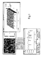
- Fig.1 is a microscope photograph (upper left) of a GaN substrate of Embodiment 1, a two-dimensional height distribution diagram (upper right) of the GaN surface and a one-dimensional height distribution graph (lower left) scanning in x-direction of Embodiment 1.
- Embodiment 1 is a 2 inch(50mm) ⁇ GaN wafer. But the microscope photograph shows a tiny rectangular part of 130 ⁇ m(x-direction) ⁇ 100 ⁇ m(y-direction) of the GaN wafer.
- the GaN substrate of Embodiment 1 was produced by preparing a (111) GaAs single crystal undersubstrate, growing a thick GaN layer on the ELO method and the facet-maintaining method on the HVPE growth or the MOC growth, eliminating the GaAs undersubstrate by aqua regia, cutting the GaN crystal by a slicer into a plurality of GaN wafers.
- the details of the GaN growing method has been described in Japanese Patent Laying Open No.2000-12900, "GaN single crystal substrate and method of producing same". Thus the description of the production method is omitted now.
- the rugged surface has been made by lapping (mechanical grinding). It may be assumed that the mechanical grinding would make many linearly continual scratches. But the fact is otherwise. Lapping makes many linear wounds in various directions by microscopic edges on the surface. Thus grooves are separated into individual isolated deep holes. Random direction cutting prevents continual grooves from surviving. The same reason denies making continual mountain ranges. Mountains and valleys are asymmetric. mountains are rather akin to quasi-uniform. Valleys are deep and localized.
- the rectangular part of 0.13mm ⁇ 0.10mm of the left upper photograph has roughness of Rms150nm and Ra117nm.
- the line part of a 0.13mm length of the left down sectional graph has roughness Rms122nm and Ra80nm which are different from the roughness of the above rectangular part.
- the present invention defines the desired quality of GaN substrates by the roughness Rms and Ra counted upon the whole of the GaN substrates.
- roughness should be measured on allover the substrate. But whole measurements of roughness take much time and cost.
- Embodiment 1 is represented by the above 0.13mm ⁇ 0.10mm rectangular part.
- the isolated holes are polygonal cones. Deep holes mean that the slanting walls of the holes are composed of low Miller index facets. Low Miller index facets form the polygonal slanting walls of the deep holes.
- the plane index of the surface is (0001), which means a C-plane.
- An epitaxially-grown film has also a surface whose normal is parallel to the c-axis. However parts having a C-plane occupy a far small rate on the surface. Almost all of the superficial parts are low Miller index facets of ⁇ 1-101 ⁇ , ⁇ 11-21 ⁇ , ⁇ 10-12 ⁇ or ⁇ 1-212 ⁇ and so on.
- the slanting walls of the holes are composed of the ⁇ 1-101 ⁇ , ⁇ 11-21 ⁇ , ⁇ 10-12 ⁇ and ⁇ 1-212 ⁇ facets.
- Dislocations extend with the crystal surface in the direction of the growth.
- Dislocations which are continual threads extending in the growing crystal, turn toward to boundaries of neighboring facets building the slanting walls.
- Dislocations are gathered to the six or twelve boundaries.
- Fig.8 shows the behavior of the dislocations in a hole prepared by the lapping process.
- the shown valley has six facets of low indexes, which is somewhat an idealized pit.
- the low index which in particular signifies the low fourth index n of (hkmn)
- n the low fourth index
- the valleys are deep holes with steep walls.
- the steep walls gather forcibly dislocations into the bottom of the pit holes.
- the strong inclination facilitates the holes to arrest the dislocations at the bottom.
- the present invention relies upon such deep valleys having steep slanting walls.
- the inclination required by the present invention to the facets is far stronger than the localized ELO proposed by M, Ishida, M. Ogawa. K. Orita, O.
- Threading dislocations are gathered and are arrested by the bottoms of valleys. Dislocation density in other parts reduces, since dislocations have been swept away to the pit bottoms.
- a film grown epitaxially on the rugged surface substrate has an advantage of low dislocation density. Namely the ruggedness of substrates reduces dislocation density of the film epitaxially grown thereupon.
- a common sense of crystal growth recommends a smooth, mirror flat substrate. This invention, which favors random-ground, rugged substrate, challenges the common sense.
- the GaN film grown epitaxially on the substrate of Embodiment 1 has roughness of Rms150nm, which means not very good morphology of the film.
- Morphology allows by the present invention has a lower limit of Rms160nm as shown at point ⁇ of Fig.7.
- the roughness Rms150nm of Embodiment 1 satisfies the requirement of morphology Rms ⁇ 160nm.
- the EPD is low enough, which satisfies the requirement.
- the present invention requires a plenty of individual separated valleys and few of individual separated mountains.
- Fig.1 lower left figure of the x-direction scanning of surface roughness shows a smaller number of isolated mountains and a larger number of isolated holes.
- Such an asymmetric mountain/hole distribution is effective to decreasing dislocations on the films epitaxially grown on the rough substrate.
- Fig.2 is a microscope photograph (upper left) of a GaN substrate of Embodiment 2, a two-dimensional height distribution diagram (upper right) of the GaN surface and a one-dimensional height distribution graph (lower left) scanning in x-direction of Embodiment 2.
- Embodiment 2 is a 2 inch(50mm) ⁇ GaN wafer.
- the microscope photograph shows a tiny rectangular part of 130 ⁇ m(x-direction) ⁇ 100 ⁇ m(y-direction) of the GaN wafer.
- the roughness of the rectangular part is Rms136.884nm and Ra103.057nm.
- the measured Rms value (137nm) is included within the range (5mm to 200mm) determined by the present invention.
- Embodiment 2 Method of producing the as-cut GaN wafer of Embodiment 2 is similar to Embodiment 1. The description of the production method is omitted.
- a thin GaN film has been grown on the rugged substrate of Embodiment 2.
- Morphology of the epitaxial film is not good.
- the EPD is low enough, of 0.9 ⁇ 10 8 cm -2 .
- Fig.2 two-dimension scanning and one-dimension scanning figures
- the number of holes is large and the area of flat parts are narrow.
- the holes have big depths with big diameter. All dislocations within a hole are united into a single dislocation bundle.
- the number of EPD of the epi-film reduces. The result confirms the surmise of dislocations of the present invention shown in Fig.8.
- Fig.3 is a microscope photograph (upper left) of a GaN substrate of Embodiment 3, a two-dimensional height distribution diagram (upper right) of the GaN surface and a one-dimensional height distribution graph (lower left) scanning in x-direction of Embodiment 3.
- Embodiment 3 is a 2 inch(50mm) ⁇ GaN wafer.
- the microscope photograph shows a small rectangular part of 130 ⁇ m(x-direction) ⁇ 100 ⁇ m(y-direction) of the GaN wafer.
- the roughness of the rectangular part is Rms117.944nm and Ra53.598nm.
- the measured Rms value (137nm) is included within the range (5mm to 200mm) determined by the present invention.
- the roughness on the x-line is bigger (about twice) than the roughness Rms and Ra on the above rectangle region. This is because the x-line includes extraordinary deep holes which appears at a left nearer region in the right 2-dimensional figure of Fig.3 by chance.
- GaN film has been grown on the rugged substrate of Embodiment 3. Morphology of the epitaxial film is improved.
- the EPD increases to 1.5 ⁇ 10 8 cm -2 .
- Fig.3 two-dimension scanning and one-dimension scanning figures
- the number of holes is reduced and the area of flat parts is raised. Since the number of holes is decreased, the surface loses a part of the power of gathering dislocations and reducing dislocation density. Then the EPD increases.
- Fig.4 is a microscope photograph (upper left) of a GaN substrate of Embodiment 4, a two-dimensional height distribution diagram (upper right) of the GaN surface and a one-dimensional height distribution graph (lower left) scanning in x-direction of Embodiment 4.
- Embodiment 4 is a 2 inch(50mm) ⁇ GaN wafer.
- the microscope photograph shows a small rectangular part of 130 ⁇ m(x-direction) ⁇ 100 ⁇ m(y-direction) of the GaN wafer.
- the roughness of the rectangular part is Rms23.709nm and Ra9.494nm.
- the measured Rms value (24nm) is included within the range (5mm to 200mm) determined by the present invention.
- the roughness on the x-line is bigger (about twice to three times) than the roughness Rms and Ra on the above rectangle region. This is because the x-line includes very extraordinary deep holes (-1.4 ⁇ -1 ⁇ m depth) , which appears at a middle lower region in the right 2-dimensional figure of Fig.4, by chance.
- the number of holes deceases.
- the depth of holes is decreases.
- GaN film has been grown on the rugged substrate of Embodiment 4. Morphology of the epitaxial film is further improved. The EPD, however, still increases to 8 ⁇ 10 8 cm -2 . As shown in Fig.4 (two-dimension scanning and one-dimension scanning figures), the number of holes is reduced and the area of flat parts is raised. Since the number of holes is further decreased, the surface loses a part of the power of gathering dislocations and reducing dislocation density. Then the EPD increases.
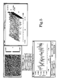
- Fig.5 is a microscope photograph (upper left) of a GaN substrate of Comparison Example 5, a two-dimensional height distribution diagram (upper right) of the GaN surface and a one-dimensional height distribution graph (lower left) scanning in x-direction of Comparison Example 5. Attention should be paid that the height scales are different from the preceding embodiments. The height scales are very small in Fig.5 for clarifying small roughness.
- Comparison Example 5 is a 2 inch(50mm) ⁇ GaN wafer.
- the microscope photograph shows a small rectangular part of 130 ⁇ m(x-direction) ⁇ 100 ⁇ m(y-direction) of the GaN wafer.
- the roughness of the rectangular part is Rms2.034nm and Ra1.610nm.
- the measured Rms value (2nm) is excluded out of the range (5 ⁇ m to 200 ⁇ m) determined by the present invention.
- GaN film has been grown on the smooth substrate of Comparison Example 5. Morphology of the epitaxial film is still further improved. The morphology is the best among five examples. The EPD, however, still increases to 2 ⁇ 10 9 cm -2 . The present invention requires the EPD below 1 ⁇ 10 9 cm -2 . The measured EPD is excluded out of the range. As shown in Fig.5 (two-dimension scanning and one-dimension scanning figures), the number and depth of holes are further reduced and the area of flat parts is enhanced. Comparison Example 5 has poor power of gathering dislocations and reducing dislocation density. Then the EPD jumps over the predetermined limit (1 ⁇ 10 9 cm -2 ).
- Changes from Fig.1 to Fig.5 are a tendency of vanishing of valleys, flattening of mountains, unification of holes and smoothing of surfaces and , which means vanishing of valleys and mountains, and accompanying tendency of increasing of EPDs on epi-layers.
- the present invention discovers that the morphology of the film epitaxially-grown on a nitride semiconductor substrate contradicts the dislocation density of the nitride semiconductor (e.g.,GaN) substrate.
- the nitride semiconductor substrate should have large roughness between Rms5nm and Rms200nm for satisfying the contradictory requirements. Larger roughness between Rms200nm to Rms100nm of the substrate with affluent valleys accelerates reduction of dislocations on the epitaxial film. Smaller roughness between Rms5nm to Rms100nm effectively improves morphology of the epitaxial film.
- Compatibility of morphology and dislocations requires the substrate roughness of Rms5nm to Rms 200nm.
- the present invention expresses the roughness by Rms, which is a root mean square of deviation ( ⁇ (x-m) 2 /N> ⁇ 1/2 ).
- the present invention can be otherwise expressed by other roughness parameters.
- Rms roughness parameters of Rmax, Ra, Rms, Ry, Rz and ⁇ m. Definitions of the parameters are different. Relations among these roughness parameters are not uniquely determined.
- Rms is an average on the whole surface of an object GaN substrate.
Landscapes
- Chemical & Material Sciences (AREA)
- Inorganic Chemistry (AREA)
- Engineering & Computer Science (AREA)
- Crystallography & Structural Chemistry (AREA)
- Materials Engineering (AREA)
- Metallurgy (AREA)
- Organic Chemistry (AREA)
- Crystals, And After-Treatments Of Crystals (AREA)
- Led Devices (AREA)
- Recrystallisation Techniques (AREA)
Abstract
Description
Such an asymmetric mountain/hole distribution is effective to decreasing dislocations on the films epitaxially grown on the rough substrate.
Claims (7)
- A nitride semiconductor substrate having a surface with roughness between Rms5nm and Rms200nm.
- A nitride semiconductor substrate having a surface with roughness between Rms50nm and Rms200nm.
- A nitride semiconductor substrate having a surface lapped by free whetting granules or fixed whetting granules to roughness between Rms5nm and Rms200nm.
- A nitride semiconductor substrate having a surface having dislocation density between 105cm-2 and 109cm-2 and being lapped by free whetting granules or fixed whetting granules to roughness between Rms5nm and Rms200nm.
- The nitride semiconductor substrate according to claim 4, wherein a process-induced transformation layer is eliminated by dry etching or wet etching after lapping the surface.
- A method of producing a nitride semiconductor substrate comprising the steps of a nitride semiconductor film on a GaAs undersubstrate by an HVPE method or an MOC method, eliminating the GaAs undersubstrate into a freestanding nitride semiconductor wafer, lapping a surface of the freestanding nitride semiconductor wafer by free whetting granules or fixed whetting granules into surface roughness between Rms5nm and Rms200nm.
- The method according to claim 6, wherein the whetting granules are stepwise changed from larger granules to smaller granules at a plural of steps and final whetting granules have average diameters between 1µm and 5µm.
Applications Claiming Priority (2)
| Application Number | Priority Date | Filing Date | Title |
|---|---|---|---|
| JP2003345910A JP2005112641A (en) | 2003-10-03 | 2003-10-03 | Nitride semiconductor substrate and method for manufacturing nitride semiconductor substrate |
| JP2003345910 | 2003-10-03 |
Publications (2)
| Publication Number | Publication Date |
|---|---|
| EP1521310A2 true EP1521310A2 (en) | 2005-04-06 |
| EP1521310A3 EP1521310A3 (en) | 2011-01-26 |
Family
ID=34309164
Family Applications (1)
| Application Number | Title | Priority Date | Filing Date |
|---|---|---|---|
| EP04021388A Withdrawn EP1521310A3 (en) | 2003-10-03 | 2004-09-08 | Nitride semiconductor substrate and method of producing same |
Country Status (8)
| Country | Link |
|---|---|
| US (2) | US7154131B2 (en) |
| EP (1) | EP1521310A3 (en) |
| JP (1) | JP2005112641A (en) |
| KR (1) | KR20050033422A (en) |
| CN (1) | CN100361323C (en) |
| CA (1) | CA2480837A1 (en) |
| NO (1) | NO20044180L (en) |
| TW (1) | TWI305061B (en) |
Families Citing this family (24)
| Publication number | Priority date | Publication date | Assignee | Title |
|---|---|---|---|---|
| US7504274B2 (en) * | 2004-05-10 | 2009-03-17 | The Regents Of The University Of California | Fabrication of nonpolar indium gallium nitride thin films, heterostructures and devices by metalorganic chemical vapor deposition |
| JP2007095975A (en) * | 2005-09-29 | 2007-04-12 | National Institute Of Advanced Industrial & Technology | Diamond power semiconductor device and manufacturing method thereof |
| KR100809243B1 (en) * | 2006-04-27 | 2008-02-29 | 삼성전기주식회사 | Nitride film production method and nitride structure |
| US7879697B2 (en) * | 2006-06-05 | 2011-02-01 | Regents Of The University Of Minnesota | Growth of low dislocation density Group-III nitrides and related thin-film structures |
| US20090053401A1 (en) * | 2007-08-24 | 2009-02-26 | Maxim Integrated Products, Inc. | Piezoelectric deposition for BAW resonators |
| US8512800B2 (en) * | 2007-12-04 | 2013-08-20 | Triquint Semiconductor, Inc. | Optimal acoustic impedance materials for polished substrate coating to suppress passband ripple in BAW resonators and filters |
| JP5560528B2 (en) * | 2008-01-28 | 2014-07-30 | 住友電気工業株式会社 | Method for producing group III nitride single crystal ingot and method for producing group III nitride single crystal substrate |
| US7781780B2 (en) * | 2008-03-31 | 2010-08-24 | Bridgelux, Inc. | Light emitting diodes with smooth surface for reflective electrode |
| US7768364B2 (en) | 2008-06-09 | 2010-08-03 | Maxim Integrated Products, Inc. | Bulk acoustic resonators with multi-layer electrodes |
| JP5104830B2 (en) * | 2008-09-08 | 2012-12-19 | 住友電気工業株式会社 | substrate |
| TW201029073A (en) * | 2009-01-21 | 2010-08-01 | Univ Nat Chunghsing | Epitaxial wafer with low surface defect density |
| JP5365454B2 (en) | 2009-09-30 | 2013-12-11 | 住友電気工業株式会社 | Group III nitride semiconductor substrate, epitaxial substrate, and semiconductor device |
| JP4513927B1 (en) | 2009-09-30 | 2010-07-28 | 住友電気工業株式会社 | Group III nitride semiconductor substrate, epitaxial substrate, and semiconductor device |
| JP5808208B2 (en) * | 2011-09-15 | 2015-11-10 | 株式会社サイオクス | Manufacturing method of nitride semiconductor substrate |
| JP6045633B2 (en) * | 2015-05-25 | 2016-12-14 | 住友化学株式会社 | Manufacturing method of nitride semiconductor substrate |
| US11370076B2 (en) * | 2016-02-23 | 2022-06-28 | Panasonic Intellectual Property Management Co., Ltd. | RAMO4 substrate and manufacturing method thereof |
| CN107855886A (en) * | 2017-11-02 | 2018-03-30 | 广东工科机电有限公司 | Dry type flexible grinding and polishing method and its supporting cutter, equipment |
| JP7231352B2 (en) * | 2018-07-31 | 2023-03-01 | 住友化学株式会社 | Manufacturing method of substrate for nitride crystal growth |
| JP6595689B1 (en) * | 2018-11-08 | 2019-10-23 | 株式会社サイオクス | Nitride semiconductor substrate manufacturing method, nitride semiconductor substrate, and laminated structure |
| JP7556197B2 (en) * | 2020-01-17 | 2024-09-26 | 東ソー株式会社 | Laminated film and its manufacturing method |
| CN114914338B (en) * | 2021-02-10 | 2025-02-07 | 纳微朗科技(深圳)有限公司 | Light emitting device and method for manufacturing the same |
| CN115125617B (en) * | 2022-08-04 | 2023-04-28 | 齐鲁工业大学 | Method for preparing self-supporting gallium nitride bulk single crystal by setting temperature gradient |
| CN115036402B (en) * | 2022-08-12 | 2022-10-25 | 江苏第三代半导体研究院有限公司 | Induction-enhanced Micro-LED homoepitaxial structure and preparation method thereof |
| CN116072533B (en) * | 2023-03-28 | 2023-06-13 | 成都功成半导体有限公司 | A wafer and wafer thinning process processing technology |
Family Cites Families (12)
| Publication number | Priority date | Publication date | Assignee | Title |
|---|---|---|---|---|
| US5679152A (en) * | 1994-01-27 | 1997-10-21 | Advanced Technology Materials, Inc. | Method of making a single crystals Ga*N article |
| JP3292083B2 (en) | 1997-03-11 | 2002-06-17 | 日亜化学工業株式会社 | Method for manufacturing nitride semiconductor substrate and method for manufacturing nitride semiconductor element |
| JP3899652B2 (en) | 1997-03-14 | 2007-03-28 | 住友電気工業株式会社 | Epitaxial wafer |
| JP3788037B2 (en) | 1998-06-18 | 2006-06-21 | 住友電気工業株式会社 | GaN single crystal substrate |
| JP4008586B2 (en) * | 1998-08-09 | 2007-11-14 | エムテック株式会社 | Work edge polishing machine |
| JP4145437B2 (en) | 1999-09-28 | 2008-09-03 | 住友電気工業株式会社 | Single crystal GaN crystal growth method, single crystal GaN substrate manufacturing method, and single crystal GaN substrate |
| US6596079B1 (en) | 2000-03-13 | 2003-07-22 | Advanced Technology Materials, Inc. | III-V nitride substrate boule and method of making and using the same |
| JP2001322899A (en) | 2000-05-11 | 2001-11-20 | Matsushita Electric Ind Co Ltd | Gallium nitride based compound semiconductor substrate and method of manufacturing the same |
| JP4156200B2 (en) * | 2001-01-09 | 2008-09-24 | 株式会社荏原製作所 | Polishing apparatus and polishing method |
| JP2002356398A (en) * | 2001-06-01 | 2002-12-13 | Sumitomo Electric Ind Ltd | Gallium nitride wafer |
| US6488767B1 (en) * | 2001-06-08 | 2002-12-03 | Advanced Technology Materials, Inc. | High surface quality GaN wafer and method of fabricating same |
| KR100550491B1 (en) * | 2003-05-06 | 2006-02-09 | 스미토모덴키고교가부시키가이샤 | Nitride semiconductor substrate and processing method of nitride semiconductor substrate |
-
2003
- 2003-10-03 JP JP2003345910A patent/JP2005112641A/en active Pending
-
2004
- 2004-07-19 TW TW093121516A patent/TWI305061B/en active
- 2004-08-26 KR KR1020040067462A patent/KR20050033422A/en not_active Ceased
- 2004-09-08 EP EP04021388A patent/EP1521310A3/en not_active Withdrawn
- 2004-09-09 CA CA002480837A patent/CA2480837A1/en not_active Abandoned
- 2004-09-22 CN CNB2004100118527A patent/CN100361323C/en not_active Expired - Fee Related
- 2004-10-01 US US10/954,186 patent/US7154131B2/en not_active Expired - Fee Related
- 2004-10-04 NO NO20044180A patent/NO20044180L/en not_active Application Discontinuation
-
2005
- 2005-11-01 US US11/262,823 patent/US7390747B2/en not_active Expired - Fee Related
Also Published As
| Publication number | Publication date |
|---|---|
| CN1604344A (en) | 2005-04-06 |
| JP2005112641A (en) | 2005-04-28 |
| KR20050033422A (en) | 2005-04-12 |
| HK1073532A1 (en) | 2005-10-07 |
| US7154131B2 (en) | 2006-12-26 |
| TW200520259A (en) | 2005-06-16 |
| CA2480837A1 (en) | 2005-04-03 |
| NO20044180L (en) | 2005-04-04 |
| US7390747B2 (en) | 2008-06-24 |
| US20050073027A1 (en) | 2005-04-07 |
| EP1521310A3 (en) | 2011-01-26 |
| CN100361323C (en) | 2008-01-09 |
| TWI305061B (en) | 2009-01-01 |
| US20060071234A1 (en) | 2006-04-06 |
Similar Documents
| Publication | Publication Date | Title |
|---|---|---|
| US7154131B2 (en) | Nitride semiconductor substrate and method of producing same | |
| US7972711B2 (en) | Large area, uniformly low dislocation density GaN substrate and process for making the same | |
| JP4696935B2 (en) | III-V nitride semiconductor substrate and III-V nitride light emitting device | |
| JP4691911B2 (en) | III-V nitride semiconductor free-standing substrate manufacturing method | |
| JP4380294B2 (en) | Group III-V nitride semiconductor substrate | |
| WO2002023604A1 (en) | Semiconductor base material and method of manufacturing the material | |
| JP2009132613A (en) | Group III-V nitride semiconductor substrate and method of manufacturing the same, group III-V nitride semiconductor device, group III-V nitride semiconductor substrate lot | |
| KR20110088483A (en) | Method for manufacturing Baan single crystal substrate and Baan single crystal substrate | |
| CN100453712C (en) | III-V nitride-based semiconductor substrate and manufacturing method thereof | |
| JP2005340747A (en) | Group III-V nitride semiconductor substrate and method of manufacturing the same, group III-V nitride semiconductor device, group III-V nitride semiconductor substrate lot | |
| JP2002329665A (en) | Method for manufacturing single substrate made of nitride semiconductor | |
| JP2009114061A (en) | III-V nitride semiconductor free-standing substrate manufacturing method | |
| JP2004335646A (en) | GaN substrate | |
| JP3985839B2 (en) | Single crystal GaN substrate | |
| EP1852897A1 (en) | Nitride semiconductor material and method for manufacturing nitride semiconductor crystal | |
| JP4003802B2 (en) | Method for growing gallium nitride crystal | |
| HK1073532B (en) | Nitride semiconductor substrate and method of producting same | |
| JP2006261649A (en) | Nitride semiconductor material and method for producing nitride semiconductor crystal | |
| HK1094484A1 (en) | Production method of gan single crystal substrate |
Legal Events
| Date | Code | Title | Description |
|---|---|---|---|
| PUAI | Public reference made under article 153(3) epc to a published international application that has entered the european phase |
Free format text: ORIGINAL CODE: 0009012 |
|
| AK | Designated contracting states |
Kind code of ref document: A2 Designated state(s): AT BE BG CH CY CZ DE DK EE ES FI FR GB GR HU IE IT LI LU MC NL PL PT RO SE SI SK TR |
|
| AX | Request for extension of the european patent |
Extension state: AL HR LT LV MK |
|
| PUAL | Search report despatched |
Free format text: ORIGINAL CODE: 0009013 |
|
| RIC1 | Information provided on ipc code assigned before grant |
Ipc: H01L 33/22 20100101ALN20101209BHEP Ipc: H01L 33/00 20100101ALN20101209BHEP Ipc: H01L 21/02 20060101ALI20101209BHEP Ipc: H01L 21/205 20060101ALI20101209BHEP Ipc: H01L 21/20 20060101ALI20101209BHEP Ipc: C30B 29/40 20060101ALI20101209BHEP Ipc: C30B 25/18 20060101AFI20101209BHEP |
|
| AK | Designated contracting states |
Kind code of ref document: A3 Designated state(s): AT BE BG CH CY CZ DE DK EE ES FI FR GB GR HU IE IT LI LU MC NL PL PT RO SE SI SK TR |
|
| AX | Request for extension of the european patent |
Extension state: AL HR LT LV MK |
|
| STAA | Information on the status of an ep patent application or granted ep patent |
Free format text: STATUS: THE APPLICATION IS DEEMED TO BE WITHDRAWN |
|
| AKY | No designation fees paid | ||
| REG | Reference to a national code |
Ref country code: DE Ref legal event code: R108 |
|
| 18D | Application deemed to be withdrawn |
Effective date: 20110331 |
|
| REG | Reference to a national code |
Ref country code: DE Ref legal event code: R108 Effective date: 20110928 |