EP1521179B1 - Phasengesteuerte Hochgeschwindigkeitschnittstellen - Google Patents
Phasengesteuerte Hochgeschwindigkeitschnittstellen Download PDFInfo
- Publication number
- EP1521179B1 EP1521179B1 EP04023594A EP04023594A EP1521179B1 EP 1521179 B1 EP1521179 B1 EP 1521179B1 EP 04023594 A EP04023594 A EP 04023594A EP 04023594 A EP04023594 A EP 04023594A EP 1521179 B1 EP1521179 B1 EP 1521179B1
- Authority
- EP
- European Patent Office
- Prior art keywords
- signals
- phase
- signal
- chip
- clock
- Prior art date
- Legal status (The legal status is an assumption and is not a legal conclusion. Google has not performed a legal analysis and makes no representation as to the accuracy of the status listed.)
- Expired - Lifetime
Links
Images


Classifications
-
- G—PHYSICS
- G11—INFORMATION STORAGE
- G11C—STATIC STORES
- G11C7/00—Arrangements for writing information into, or reading information out from, a digital store
- G11C7/04—Arrangements for writing information into, or reading information out from, a digital store with means for avoiding disturbances due to temperature effects
-
- G—PHYSICS
- G06—COMPUTING OR CALCULATING; COUNTING
- G06F—ELECTRIC DIGITAL DATA PROCESSING
- G06F13/00—Interconnection of, or transfer of information or other signals between, memories, input/output devices or central processing units
- G06F13/38—Information transfer, e.g. on bus
- G06F13/42—Bus transfer protocol, e.g. handshake; Synchronisation
- G06F13/4204—Bus transfer protocol, e.g. handshake; Synchronisation on a parallel bus
- G06F13/4234—Bus transfer protocol, e.g. handshake; Synchronisation on a parallel bus being a memory bus
- G06F13/4243—Bus transfer protocol, e.g. handshake; Synchronisation on a parallel bus being a memory bus with synchronous protocol
-
- G—PHYSICS
- G11—INFORMATION STORAGE
- G11C—STATIC STORES
- G11C11/00—Digital stores characterised by the use of particular electric or magnetic storage elements; Storage elements therefor
- G11C11/21—Digital stores characterised by the use of particular electric or magnetic storage elements; Storage elements therefor using electric elements
- G11C11/34—Digital stores characterised by the use of particular electric or magnetic storage elements; Storage elements therefor using electric elements using semiconductor devices
- G11C11/40—Digital stores characterised by the use of particular electric or magnetic storage elements; Storage elements therefor using electric elements using semiconductor devices using transistors
- G11C11/401—Digital stores characterised by the use of particular electric or magnetic storage elements; Storage elements therefor using electric elements using semiconductor devices using transistors forming cells needing refreshing or charge regeneration, i.e. dynamic cells
- G11C11/4063—Auxiliary circuits, e.g. for addressing, decoding, driving, writing, sensing or timing
- G11C11/407—Auxiliary circuits, e.g. for addressing, decoding, driving, writing, sensing or timing for memory cells of the field-effect type
- G11C11/4076—Timing circuits
-
- G—PHYSICS
- G11—INFORMATION STORAGE
- G11C—STATIC STORES
- G11C11/00—Digital stores characterised by the use of particular electric or magnetic storage elements; Storage elements therefor
- G11C11/21—Digital stores characterised by the use of particular electric or magnetic storage elements; Storage elements therefor using electric elements
- G11C11/34—Digital stores characterised by the use of particular electric or magnetic storage elements; Storage elements therefor using electric elements using semiconductor devices
- G11C11/40—Digital stores characterised by the use of particular electric or magnetic storage elements; Storage elements therefor using electric elements using semiconductor devices using transistors
- G11C11/401—Digital stores characterised by the use of particular electric or magnetic storage elements; Storage elements therefor using electric elements using semiconductor devices using transistors forming cells needing refreshing or charge regeneration, i.e. dynamic cells
- G11C11/4063—Auxiliary circuits, e.g. for addressing, decoding, driving, writing, sensing or timing
- G11C11/407—Auxiliary circuits, e.g. for addressing, decoding, driving, writing, sensing or timing for memory cells of the field-effect type
- G11C11/409—Read-write [R-W] circuits
- G11C11/4093—Input/output [I/O] data interface arrangements, e.g. data buffers
-
- G—PHYSICS
- G11—INFORMATION STORAGE
- G11C—STATIC STORES
- G11C29/00—Checking stores for correct operation ; Subsequent repair; Testing stores during standby or offline operation
- G11C29/02—Detection or location of defective auxiliary circuits, e.g. defective refresh counters
-
- G—PHYSICS
- G11—INFORMATION STORAGE
- G11C—STATIC STORES
- G11C29/00—Checking stores for correct operation ; Subsequent repair; Testing stores during standby or offline operation
- G11C29/02—Detection or location of defective auxiliary circuits, e.g. defective refresh counters
- G11C29/022—Detection or location of defective auxiliary circuits, e.g. defective refresh counters in I/O circuitry
-
- G—PHYSICS
- G11—INFORMATION STORAGE
- G11C—STATIC STORES
- G11C29/00—Checking stores for correct operation ; Subsequent repair; Testing stores during standby or offline operation
- G11C29/02—Detection or location of defective auxiliary circuits, e.g. defective refresh counters
- G11C29/023—Detection or location of defective auxiliary circuits, e.g. defective refresh counters in clock generator or timing circuitry
-
- G—PHYSICS
- G11—INFORMATION STORAGE
- G11C—STATIC STORES
- G11C29/00—Checking stores for correct operation ; Subsequent repair; Testing stores during standby or offline operation
- G11C29/02—Detection or location of defective auxiliary circuits, e.g. defective refresh counters
- G11C29/028—Detection or location of defective auxiliary circuits, e.g. defective refresh counters with adaption or trimming of parameters
-
- G—PHYSICS
- G11—INFORMATION STORAGE
- G11C—STATIC STORES
- G11C7/00—Arrangements for writing information into, or reading information out from, a digital store
- G11C7/10—Input/output [I/O] data interface arrangements, e.g. I/O data control circuits, I/O data buffers
- G11C7/1051—Data output circuits, e.g. read-out amplifiers, data output buffers, data output registers, data output level conversion circuits
- G11C7/1066—Output synchronization
-
- G—PHYSICS
- G11—INFORMATION STORAGE
- G11C—STATIC STORES
- G11C7/00—Arrangements for writing information into, or reading information out from, a digital store
- G11C7/22—Read-write [R-W] timing or clocking circuits; Read-write [R-W] control signal generators or management
-
- G—PHYSICS
- G11—INFORMATION STORAGE
- G11C—STATIC STORES
- G11C7/00—Arrangements for writing information into, or reading information out from, a digital store
- G11C7/22—Read-write [R-W] timing or clocking circuits; Read-write [R-W] control signal generators or management
- G11C7/222—Clock generating, synchronizing or distributing circuits within memory device
-
- H—ELECTRICITY
- H03—ELECTRONIC CIRCUITRY
- H03L—AUTOMATIC CONTROL, STARTING, SYNCHRONISATION OR STABILISATION OF GENERATORS OF ELECTRONIC OSCILLATIONS OR PULSES
- H03L7/00—Automatic control of frequency or phase; Synchronisation
- H03L7/06—Automatic control of frequency or phase; Synchronisation using a reference signal applied to a frequency- or phase-locked loop
- H03L7/08—Details of the phase-locked loop
- H03L7/0805—Details of the phase-locked loop the loop being adapted to provide an additional control signal for use outside the loop
-
- H—ELECTRICITY
- H03—ELECTRONIC CIRCUITRY
- H03L—AUTOMATIC CONTROL, STARTING, SYNCHRONISATION OR STABILISATION OF GENERATORS OF ELECTRONIC OSCILLATIONS OR PULSES
- H03L7/00—Automatic control of frequency or phase; Synchronisation
- H03L7/06—Automatic control of frequency or phase; Synchronisation using a reference signal applied to a frequency- or phase-locked loop
- H03L7/08—Details of the phase-locked loop
- H03L7/081—Details of the phase-locked loop provided with an additional controlled phase shifter
- H03L7/0812—Details of the phase-locked loop provided with an additional controlled phase shifter and where no voltage or current controlled oscillator is used
-
- H—ELECTRICITY
- H03—ELECTRONIC CIRCUITRY
- H03L—AUTOMATIC CONTROL, STARTING, SYNCHRONISATION OR STABILISATION OF GENERATORS OF ELECTRONIC OSCILLATIONS OR PULSES
- H03L7/00—Automatic control of frequency or phase; Synchronisation
- H03L7/06—Automatic control of frequency or phase; Synchronisation using a reference signal applied to a frequency- or phase-locked loop
- H03L7/16—Indirect frequency synthesis, i.e. generating a desired one of a number of predetermined frequencies using a frequency- or phase-locked loop
- H03L7/18—Indirect frequency synthesis, i.e. generating a desired one of a number of predetermined frequencies using a frequency- or phase-locked loop using a frequency divider or counter in the loop
- H03L7/183—Indirect frequency synthesis, i.e. generating a desired one of a number of predetermined frequencies using a frequency- or phase-locked loop using a frequency divider or counter in the loop a time difference being used for locking the loop, the counter counting between fixed numbers or the frequency divider dividing by a fixed number
-
- H—ELECTRICITY
- H03—ELECTRONIC CIRCUITRY
- H03L—AUTOMATIC CONTROL, STARTING, SYNCHRONISATION OR STABILISATION OF GENERATORS OF ELECTRONIC OSCILLATIONS OR PULSES
- H03L7/00—Automatic control of frequency or phase; Synchronisation
- H03L7/06—Automatic control of frequency or phase; Synchronisation using a reference signal applied to a frequency- or phase-locked loop
- H03L7/16—Indirect frequency synthesis, i.e. generating a desired one of a number of predetermined frequencies using a frequency- or phase-locked loop
- H03L7/22—Indirect frequency synthesis, i.e. generating a desired one of a number of predetermined frequencies using a frequency- or phase-locked loop using more than one loop
- H03L7/23—Indirect frequency synthesis, i.e. generating a desired one of a number of predetermined frequencies using a frequency- or phase-locked loop using more than one loop with pulse counters or frequency dividers
-
- G—PHYSICS
- G11—INFORMATION STORAGE
- G11C—STATIC STORES
- G11C11/00—Digital stores characterised by the use of particular electric or magnetic storage elements; Storage elements therefor
- G11C11/21—Digital stores characterised by the use of particular electric or magnetic storage elements; Storage elements therefor using electric elements
- G11C11/34—Digital stores characterised by the use of particular electric or magnetic storage elements; Storage elements therefor using electric elements using semiconductor devices
- G11C11/40—Digital stores characterised by the use of particular electric or magnetic storage elements; Storage elements therefor using electric elements using semiconductor devices using transistors
- G11C11/401—Digital stores characterised by the use of particular electric or magnetic storage elements; Storage elements therefor using electric elements using semiconductor devices using transistors forming cells needing refreshing or charge regeneration, i.e. dynamic cells
-
- H—ELECTRICITY
- H03—ELECTRONIC CIRCUITRY
- H03K—PULSE TECHNIQUE
- H03K5/00—Manipulating of pulses not covered by one of the other main groups of this subclass
- H03K2005/00013—Delay, i.e. output pulse is delayed after input pulse and pulse length of output pulse is dependent on pulse length of input pulse
- H03K2005/00019—Variable delay
- H03K2005/00026—Variable delay controlled by an analog electrical signal, e.g. obtained after conversion by a D/A converter
- H03K2005/00052—Variable delay controlled by an analog electrical signal, e.g. obtained after conversion by a D/A converter by mixing the outputs of fixed delayed signals with each other or with the input signal
Definitions
- the present invention is related to high speed interfaces.
- Double Data Rate (DDR) Dynamic Random Access Memories are used in many systems, such as chips in set top boxes.
- DDR DRAM Double Data Rate Dynamic Random Access Memories
- clock and strobe signals should be positioned accurately within address, control, and data signals.
- DDR clock cycles there are two data signals per cycle, one per half cycle. It is usually desired to strobe data when the data cycle is stable within the half cycle, for example in the middle of the half cycle. Strobing a data signal at a stable point is needed to read or write data correctly to the DDR DRAM.
- MUX multiplexer
- buffers that can generate a variable number of delays.
- a chain of buffers or inverters are used for each delay, for example, one buffer may provide 10ps of delay, 2 buffers 20ps, etc.
- the MUX has paths for one, two, three, etc. intervals of delays, so the strobe signal can be delayed by, for example, 10 ps, 20 ps, 30 ps, etc. depending on a path chosen in the MUX.
- DLL delay locked loop
- DLL delay locked loop
- the buffers operate as desired until data rates reach 133-150MHz. Although the buffers give some coarseness and are not ideally controlled, they are sufficient for lower data rate implementations (e.g., below 200 MHz). However, buffer delay elements do not have ideal process, temperature, and voltage (PTV) variation controls, so their output values can vary based on these factors. Another problem is that at higher data rates (e.g., 200MHz and above), a window for reading and writing data is smaller, for example at 200MHz the window is 2.5 ns compared to 3.5 ns at 133MHz. So, the accuracy of the positioning of the strobe needs to be very accurately controlled at higher data rates. However, buffers can be non-ideal at these data rates, and may not accurately position the strobe signal with respect to the data signal.
- PTV process, temperature, and voltage
- US-A-5 485 490 describes a method and circuitry for clock synchronization, in particular, for performing fine phase adjustment within a phase locked loop.
- the phase selector selects an even phase signal and an odd phase signal from the twelve phase signals output by the VCO. the even and odd phase signals are selected by an even select signal and an odd select signal, respectively.
- the phase interpolator interpolates between the even phase signal and the odd phase signal to generate an output signal. The affect of the even phase signal and the odd phase signal on the output signal is determined by an even weighting signal and an odd weighting signal, respectively.
- the weighting signals prevent glitches from appearing on the output signal when either the even phase signal or the odd phase signal is switching.
- US 2001/025350 A1 concerns a synchronous circuit having a clock input for supplying a first clock signal and a clock generator being phase-locked with respect to the first clock signal.
- the clock output of the clock generator is connected to a control input of a data transmission unit used for outputting data from the circuit and/or for reading into the circuit essentially in synchronism with the first clock signal.
- the clock generator has at least two control loops connected in succession which are used for controlling the phase angle of the second clock signal, the first control loop being used to generate from the first clock signal at least two intermediate clock signals, each of which has a particular phase angle with respect to the first clock signal, and the second control loop being used to generate the second clock signal from the intermediate clock signals.
- the first control loop is deactivated during the transmission of data by the data transmission unit, so that the control of the phase angle of the intermediate clock signals is interrupted.
- An embodiment of the present invention provides a system including a chip coupled to an external device having write data path (or mode) including an analog device that receives a clock signal and generates strobe signals having a same or different frequency and a same or different phases, the strobe signals being used to correctly position output address, control, and data signals to an off-chip device and a chip read data path (or mode) including an analog delay device that processes input strobe signals from the off-chip device to correctly position the strobe signals, which are used to write input data into a storage device in the chip, a phase lock loop that receives the clock signal and outputs a plurality of first signals, phase interpolators that receive respective ones of the first signals and generate the first set of strobe signals therefrom; and a bus that carries the first signals from the phase lock loop to the phase interpolators, wherein the system is adapted to produce multiple outputs from a single PLL, wherein a first output is used to clock internal devices of the chip (100) phasing-the address and control clock
- Another embodiment of the present invention provides analog design techniques of phase interpolation for accurately positioning clock and strobe signals that are required for high speed interfaces to communicate with external devices, for example, storage devices, DDR DRAMS, etc.
- the design incorporates a PLL with multiple phased outputs that can be controlled digitally, a deskew PLL for clock alignment of the controller circuitry to the interface circuitry, and a phase interpolated voltage controlled delay line for phase shifting incoming signals.
- a further embodiment of the present invention provides a system including an interface configured to allow reading and writing to external devices (e.g. DDR DRAMS).
- the system includes a phase lock loop (PLL) (e.g., a Frac-N PLL synthesizer) configured to receive a clock signal to generate a PLL output signal and a phase interpolator device (e.g., Divider/Phase Interpolator) configured to receive a control value and the PLL output signal to generate a control clock signal.
- PLL phase lock loop
- a phase interpolator device e.g., Divider/Phase Interpolator
- Timing of a strobe signal output from the interface is controlled using the control clock signal, such that the strobe signal occurs during a stable part of the data signal during the reading and writing.
- a still further embodiment of the present invention provides using analog design techniques of phase interpolation for accurately positioning clocks and strobe signals that are required for high speed interfaces like DDR.
- the design incorporates a PLL with multiple phased outputs that can be controlled digitally, a deskew PLL for clock alignment of the controller circuitry to the interface circuitry, and a phase interpolated voltage controlled delay line for phase shifting incoming signals.
- a system including a chip coupled to an external device is provided, the system comprising:
- FIG. 1 shows a circuit including a chip having an analog and digital device communicating via a pad with a DDR DRAM according to an embodiment of the present invention.
- FIG. 2 is a block diagram of a high speed interface of the chip according to an embodiment of the present invention.
- FIGS. 3 and 4 show a write data path and timing diagram, respectively, for the high speed interface in FIG. 1 according to an embodiment of the present invention.
- FIGS. 5 and 6 show a read data path and timing diagram, respectively, for the high speed interface in FIG. 1 according to an embodiment of the present invention.
- FIG. 7 is a block diagram of a PLL in FIG. 2 according to an embodiment of the present invention.
- FIG. 8 is a schematic and block diagram of a PLL and phase interpolators in FIGS. 2 and 3 according to an embodiment of the present invention.
- FIG. 9 show ports of a deskew PLL in FIG. 2 according to an embodiment of the present invention.
- FIG. 10 is a schematic and block diagram of the deskew PLL in FIGS. 2 and 9 according to an embodiment of the present invention.
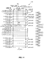
- FIG. 11 shows details of one of eight byte slices in FIG. 2 according to an embodiment of the present invention.
- FIG. 12 shows delay paths in a read data path according to an embodiment of the present invention.
- FIG. 13 shows a combined schematic and block diagram of FIGS. 7 and 9 where two clocks are used for two test clock signals according to an embodiment of the present invention.
- FIG. 14 is a portion of FIG. 13 with only one clock according to an embodiment of the present invention.
- FIG. 15 shows a phase interpolator of FIG. 8 according to an embodiment of the present invention.
- One or more embodiments of the present invention use an analog system including a phase locked-loop (PLL) with phase interpolators to produce control clock signals to properly position a strobe signal to strobe data signals without effecting stability of the data signal.
- the phase interpolators can be analog devices that produce clock control signals used to delay the strobe signal for discrete time periods.
- using analog techniques can allow for a substantial reduction in variations caused by process, temperature, and voltage (PVT), so the strobe position is more accurately controlled than a digital approach.
- PVT process, temperature, and voltage
- the present invention can also be used for clock adjustment, so that clocks are positioned correctly with respect to address and control lines.
- FIG. 1 shows a circuit 100 including a chip 102 and an external device 104 (e.g., a storage device, a memory, a DDR DRAM, or any other device requiring a high speed interface) according to an embodiment of the present invention.
- Chip 102 includes a digital signal system 106 (digital section), an analog signal system 108 (analog section), and a pad 110 (e.g., one or more unidirectional and/or bidirectional pads).
- Pad 110 is used for signal transmission between chip 102 and DDR DRAM 104 in read and write modes. In one example, a 64 bit data signal is read from or written to DDR DRAM 104.
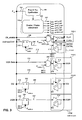
- FIG. 2 is a block diagram of chip 102 according to an embodiment of the present invention.
- a portion of digital section 106 is shown in FIG. 2 that receives signals (e.g., signals 236, 238, 212, 214, 216, 218, 220, and other signals, discussed in detail below) from another portion of digital section 106 having a memory controller or sequencer (not shown).
- the portion of digital section 106 not shown can also include other digital devices, which would become apparent to one of ordinary skill in the art upon reading this description.
- Analog section 108 includes a PLL 200 (e.g., Frac-N PLL 300 with divider/phase interpolator 302 as shown in FIGS. 3, 7 and 8) that generates clock signals FDDR1-FDDR6 202-1 to 202-6.
- Signals 202-2 and 202-3 can control even byte signals (e.g., 0, 2, 4, ....), while 202-5 and 202-6 can control odd byte signals (e.g., 1, 3, 5, ...) signals.
- PLL 200 is used to generate six clock signals FDDR1-FDDR6 202-1 to 202-6 from a single clock signal Fref 304 (FIG. 3).
- the six clock signals FDDR1-FDDR6 202-1 to 202-6 all have a same frequency, which may be a multiple of Fref 304, but are phase-adjusted with respect to each other, as shown in FIGS. 3 and 8.
- the phase adjustment amounts are based on control signals determined during testing and/or monitoring of reading and writing of data to and from DDR DRAM 104 as the data is varied.
- Analog section 108 also includes a deskew PLL 204 that aligns a clock of control circuitry with a clock of interface circuitry (see also FIGS. 9-10).
- Signal FDDR1 202-1 is used as a reference signal that is input to deskew PLL 204.
- Deskew PLL 204 also receives a clock signal Fct 206 from a clock tree 900 (FIG. 9) that is within chip 102.
- Deskew PLL 204 generates an output clock signal Flogic 208.
- Deskew PLL 204 aligns signal Fct 206 to signal FDDR1 202-1 through a determination of the delay imposed on signal Flogic 208 by clock tree 900 (FIG. 9).
- signal Flogic 208 is an adjusted signal that takes into account delay caused by clock tree 900.
- Signal Flogic 208 is received at a top portion of the clock tree 900.
- Analog section 108 further includes an eight byte slice device 210. Details of one portion (one byte) 1100 (FIG. 11) of eight byte slice device 210 are shown in FIGS. 11-12 and discussed in relation thereto.
- the present invention is applicable to, among other things, DDR memory interfaces, such as on a BCM7038 chip manufactured by Broadcom, Inc. of California.
- This type of interface can require precise control of clocks and strobing signals. As the speed of the interface increases, the accuracy of positioning the necessary strobe and clock signals with respect to the data signals becomes more stringent.
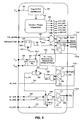
- FIGS. 3 and 4 show a write data path and timing diagram, respectively, in analog device 108 according to an embodiment of the present invention.
- FIG. 3 also shows a plurality of pads 110-A to 110-E.
- pad 110-A is unidirectional, while pads 110-B to 110-E are all bidirectional pads.
- Unidirectional pad 110-A includes a driver 306 and two pins CLKi and CLKbi.
- Bidirectional pads 110-B to 110-E all include drivers (drivers 308-314, respectively), receivers (receivers 316-322, respectively), and pins (pins ADDR/CNTRL, DQSi, DQi, and DQMi, respectively).
- Clock enable signal 236 determines when gate 240 will pass signal 202-4 to driver 306 and out pin CLKi and CLKbi. In this embodiment, only when clock enable signal 236 is HIGH can signal 202-4 pass through gate 240.
- Signal 202-1 controls when address and control signal 238 can be transmitted to pad 110-B. Address and control signal 238 is latched and delayed in flip-flop 242 until signal 202-1 releases signal 238' from flip-flop 242.
- DQS enable signal 212 controls enabling of driver 310, which controls when signal 202-2 (even bytes) or 202-5 (odd bytes) will be output to pins DQSi.
- DQS gate signal 214 controls when DQSi signals 202-2/5 pass through gate 230 to be output through pin DQSi. Signals 202-2/5 can only pass through gate 230 when gate signal 214 is HIGH.
- Signals 202-3 (even bytes) or 202-6 (odd bytes) control when data signal DQ 218 can be transmitted to pad 110-D.
- Data signal 218 is latched and delayed in flip-flop 232 until one of signals 202-3 or 202-6 release signal 218' from flip-flop 232.
- signal 202-3 controls even bytes
- signal 202-6 controls odd bytes.
- DQ enable signals 216 controls enabling of driver 312, which controls when data signal DQj 218' can be output from pad 110-D.
- Signals 202-3/6 also control when data mask signal DQM 220 can be transmitted to pad 110-E.
- Data mask signal 220 is latched and delayed in flip-flop 234 until one of signals 202-3 or 202-6 releases signal 220' from flip-flop 234.
- Data mask signal 220/220' is used to mask data during writing and/or reading, when desired, for example during invalid bursts.
- CLK_enable signal 236 (clock) and address and control signal 238 are output to pad 110.
- Clock signal 236 is controlled by FDDR4 202-4 via AND gate 240 and address and control signal 238 is controlled by FDDR1 202-1 via flip-flop 242.
- FIGS. 5 and 6 show a read data path and timing diagram, respectively, for analog device 108 according to an embodiment of the present invention.
- drivers 306-312 respectively, are disabled so pads 110-C and 110-D all receive signals and forward those received signals. More details of one embodiment of the read data path are shown in FIGS. 11-12, and described in relation thereto.
- a strobe signal 244 from DDR DRAM 104 is received at pad 110-C, which is forward via receiver 318.
- a gate 504 controls transmission of signal 244 using a read control signal 250 (e.g., rd_cmd) transmitted from gate control 252.
- Signal 244 is only transmitted through gate 504 when read control signal 250 is HIGH.
- signal 244 is delayed using delay line DL 502 to form delayed signal 244'.
- Delay line 502 receives a control signal 500 from a delay locked loop (DLL) 503.
- DLL delay locked loop
- a data signal 246 is received at pad 110-D and forward via receiver 320. Delayed signal 244' and a write pointer signal 508 are used to strobe and write a strobed data signal 246 into a storage 248 (e.g., a first-in-first-out (FIFO) memory).
- a read pointer signal 510 is used to control reading from storage 248, e.g., read pointer signal 510 can be used to access data 254 stored in a desired section of storage 248.
- FIG. 7 is a block diagram of PLL 200 according to an embodiment of the present invention.
- a differential digital clock signal 700 e.g., i_ref_ddrclk n/p, such as a 54 MHz differential clock signal
- device 704 e.g., a Diff2single device
- multiplexer 706 receives a control signal 708 to control which path (0 or 1) passes a signal.
- testing/bypass operation path 0 can pass signal 702 to PLL 300
- testing/bypass operation path 1 can pass testing/bypass signal 710 (e.g., i_byp_clk_pll, such as a 58 MHz or lower clock signal) to PLL 300.
- testing/bypass signal 710 e.g., i_byp_clk_pll, such as a 58 MHz or lower clock signal
- Phase interpolator 302 uses these input signals 714 and 716 to generate six output clock signals 718-1 to 718-6 (e.g., o_fddrn_clk).
- the clock signals 718-1 to 718-6 have a same frequency, but are phase shifted with respect to each other.
- a multiplexer 720 can be used to allow clock signals 718 along path 0 during normal operations or testing/bypass signal 722 (e.g., i_byp_clk_ph_int, such as a 200 MHz external clock signal) along path 1 during testing/bypass operation.
- Multiplexer 720 receives a signal 724 (e.g., i_bypass_pll) at its control port to control which path (0 or 1) passes an input signal (718 or 722).
- the signals being received or transmitted through respective ports in FIG. 7 can have the following characteristics:
- o_fddrl_clk 0 deg +/- 45 deg (for Addr/ctrl)
- o_fddr2_clk 0 deg +/-90deg (for Write DQS even bytes for byte staggering)
- o_fddr3_clk 90 deg +/- 45 deg (for Write DQ even bytes for byte staggering)
- o_fddr4_clk 0 deg +/- 45 deg (for clock)
- o_fddr5_clk 0 deg +/- 90 deg (for Write DQS odd bytes for byte staggering)
- o_fddr6_clk 90 deg +/- 45 deg (for Write DQ odd bytes for byte staggering)
- FIG. 8 is a schematic and block diagram of PLL 300 and phase interpolator 302 according to an embodiment of the present invention.
- PLL 300 includes phase-frequency detector/charge pump 800 (PFD/CP), a loop filter 802, a voltage controlled oscillator 804, and a feedback loop 806 that includes first and second dividers 808 and 810.
- Phase interpolator 302 includes six branches 820 each having a phase interpolator 822 and a divider 824.
- Each phase interpolator 822 selects two phases of clock signals 714 under control of control signal 716 and produces an adjusted or moved phase of clock signals 826, which is a weighted average of the two phases of the two clock signals 714 based on control signal 716 (e.g., PHn), discussed in more detail below with respect to FIG. 15.
- a phase-shifted signal 826 is divided in divider 824 (e.g., an 8 way divider) and output as FDDR 202.
- phase interpolators 822 Using phase interpolators 822, clock signals 714 are given a base line phase shift of either 0 or 90 degrees and then fine tuned to +/- 45 degrees or +/- 90 degrees, depending on where the FDDR signal is being transmitted to (see FIGS. 2, 3, and 5). In one embodiment, the default phase control values produce 0 degrees for signals FDDR1,2,4,5 and 90 degrees for signals FDDR3,6.
- the resolution for the phase controls is 2.8125 degrees
- 5-bit controls can vary the phase +/-45 degrees
- 6-bit controls can vary the phase +/-90 degrees.
- the default reset value is "10000"
- the default reset value is "100000”.
- FIG. 9 show ports of deskew PLL 204.
- deskew PLL 204 receives FDDR1 202-1 (e.g., i_ref_clk) as a reference signal at deskew PLL 902 to align Fct 206 (e.g., i_tree_clk).
- a multiplexer 904 can be used to allow for testing/bypass mode, which is controlled at its control terminal using signal 906 (e.g., i_bypass_pll).
- signal 906 e.g., i_bypass_pll
- channel 0 routes signal 208 to clock tree 900, however when in test/bypass mode, channel 1 passes signal 908 (e.g., i_byp_clk_deskew) to clock tree 900.
- FIG. 10 is a schematic and block diagram of deskew PLL 204 according to an embodiment of the present invention.
- Deskew PLL 204 includes dividers 1000 and 1002, phase-frequency detector/charge pump 1004, loop filter 1006, voltage controlled oscillator 1008, and dividers 1010 and 1012.
- FIG. 11 shows details of one of eight byte slices 1100, which are arranged to make up eight byte slice device 210 in FIG. 2.
- Each byte slice 1100 receives 8 sets of signals or bits. In write mode, several of these bits feed through byte slice 1100 without being processed. In read mode, bits are passed through delay devices 502 and 1201 (shown only in FIG. 12). The boxes on the far right side of the figure are portions of pad 110 being used to transmit and receive signals between chip 102 and DDR DRAM 104.
- FIG. 12 in which a read data flow is shown in a reverse direction to the other figures, is a schematic diagram of a read data path including a strobe signal phase control system 1200 according to an embodiment of the present invention.
- data 246 is received from DDR DRAM 104 (FIG. 1) via the left side and transmitted to digital system 106 (FIG. 1) via the right side, or opposite all other figures.
- Data signals 246 e.g., i_pad2io_dq
- delay devices 1201 e.g., one or more buffers 1208 and T/8 delay devices (voltage control delay lines (VCDLs) 1102) delaying by T/8, T being the clock period).
- VCDLs voltage control delay lines
- strobe signals 244 (e.g., i_pad2io_dqs) are transmitted based on gate signal 250 (e.g., i_d2io_gate_dqsr) at AND gate 504 before reaching delay line 502.
- Signals 244 can be delayed by an adjustable amount from 0-180 degrees, with 90 degrees being the nominal value using multiple T/8 delay devices 1202 that are delay locked (e.g., have a fixed delay).
- the control for the adjustment is a signal 1204 (e.g., i_dqsr_ph, possibly a digital signal).
- the variation in phase delay is achieved with an analog phase interpolator 1206.
- the phase adjusted signal 244' (e.g., o_io2d_dqs) is used to strobe data 246 into storage 248 (FIGS. 2 and 5).
- the T/8 plus selectable fixed delay device 1208 in the data signal path permits strobe signal 244' to be swept beyond the beginning and end of the stable data half cycle time, which allows a sweep calibration procedure to accurately position strobe 244' at an optimal point in the data value/window for strobing into storage 248.
- the sweep calibration involves writing and reading from DDR 104 till failure is observed at extremes of the sweep.
- DLL 503 generates a voltage reference input 500 to lock all T/8 delays 1202.
- a final delay value can be used for phase interpolation using phase interpolator 1206.
- system 100 positions strobe signal 244 to produce an output signal 244' (e.g., o_io2d_dqs) from driver 1210, which is used inside chip 102 to strobe data 246. So, an input strobe signal 244 is received and is delayed by some amount before reaching phase interpolator 1206. Then strobe signal 244' is used to actually latch the data 246 when reading from other chips 104.
- FIG. 13 shows a combined schematic and block diagram of FIGS. 7 and 9 where clock signals 710 and 908 are used for two test clock signals according to an embodiment of the present invention.
- FIG. 14 is a portion of FIG. 13, with additional circuitry compared to FIG. 13 according to an embodiment of the present invention.
- either two test clocks can be used or only one clock that is adjusted with device 1400, which is a numerically controlled delay line of the buffer type that may only be used for test purposes.
- Section 1402 is in analog deskew pll and connected as shown.
- a first mode is where two clocks are used that are received at pins DDR_CLK and CKE (default mode).
- a second mode is where the numerically controlled delay line (NCDL) is used with a single clock that is received at pin DDR_CLK.
- a third mode is where one clock is used that is received at pin DDR_CLK and deskew pll 902 is working normally.
- FIG. 15 shows the phase interpolator 822 of FIG. 8 according to one embodiment of the present invention.
- the phase interpolator 822 performs a weighted sum of the two input clock signals 714 ⁇ 1 and 714 ⁇ 2 , which are shifted in phase with respect to each other by less than 45 degrees.
- a weighting factor 716 ⁇ is digitally controlled.
- the resulting output clock 1502 ⁇ out has a phase, which is the weighted mean of the input clock phases.
- an analog module 108 provides general clock synthesis usable in WRITE mode timing control and READ mode timing control for the DDR I/O interface.
- Clock synthesizer PLL 200 receives, for example, a 54 MHz differential reference clock 700 and produces six independent DDR output clocks FDDR1-6 202-1 to 202-6 with programmable frequency ranges from 100 MHz to 202 MHz. All six output clocks FDDR1-6 202-1 to 202-6 have digital phase control using 5 or 6 bit inputs.
- Clock synthesizer PLL 200 outputs are received at zero insertion (deskew) PLL 204, DLL 503, read path DQS phase control system 1200, and additional digital logic circuits for write DQS, DQ, and DQM.
- the zero insertion deskew PLL 204 output Flogic 208 is advanced from the feedback return input Fct 206 to compensate for delay path 900 in the memory controller or sequencer of digital logic section 106 that supplies at least signals 236, 238, 212, 214, 216, 218, and 220.
- the DLL 503 provides master timing control for digital programmable delay line 502 in strobe signal phase control system 1200.
- the delayed DQS_OUT 244' signal clocks the data 246 into memory 248, which outputs a 8-bit data word.
- the complete 64-bit DDR DQ word uses 8 strobes in the 8 byte slices 1100.
- DLL 503 is included with each of the 8 phase control systems 1202. These systems 1202 are analog for better PVT control as DDR speeds get to 200MHz and beyond.
- FIGS. 7 and 8 show the PLL 300 that supplies 6 clock signals FDDR 202-1 to 202-6, each of which can be phase adjusted independently using the phase interpolators 822, as discussed above.
- clock positioning using phase interpolation can be done independently from most if not all of the digital circuitry being used because system 200 produces multiple outputs 202 from a single PLL 300.
- a first output 202-1 can be used to clock internal devices of a chip 102 phasing the address and control clock (FIG. 5), and a second output 202-4 can be independently positioned and transmitted to pad 110 to be transmitted outside chip 102.
- system 200 of the present invention can allow for independent control of external and internal clocks, strobes, and data.
- phase interpolators 822 receive a common input signal 714 from PLL 300.
- Phases adjustments for phase interpolator output signals 202 can be set up independently from one PLL 300.
- FDDR4 202-4 can be transmitted outside chip 102 producing it, and FDDR1 202-1 can be used inside chip 102. If FDDR1 202-1 is used inside chip 102, phase from chip 102 can be a certain value for address and control signals.
- a user can independently, for each particular design, tune FDDR1 202-1 to adjust it to be optimal for the address and control lines coming out of chip 102. This can be done while also taking into account the value of FDDR2 202-2 that was used internally in chip 102.
- the independent control of FDDR values 202 using the phase interpolators 822 allows independent tuning of internal and external strobe clock signals DQSi. Also, using phase interpolators 822 instead of digital delay lines allows for more accurately positioning of strobe, address, and control signals by substantially eliminating variations caused by process, temperature, and voltage.
- phase interpolators 822 can be used that allow delay of the strobe signal by 90 degrees +/- some desired amount.
- the strobe signal can be bi-directional signal. When writing to a DDR device 104 outside chip 102 on which the strobe is generated, the strobe needs to be positioned around 90 degrees from the start of the data, or at any good stable point. This can be accomplished using the phase interpolators 822 that produce independent clock controls 202 associated with the strobe signal DQSi transmitted external to the chip 102.
- the sending chip 104 supplies the strobe signal.
- the received strobe signal is aligned with received data, which means that when data changes the strobe changes. So, the system 100 internally shifts the strobe signal to an appropriate stable data point before strobing the data. Otherwise, the receiving chip might strobe the data while the data is changing. Chip 102 does this using voltage controlled delay lines.
- timing models that are compatible with layout extraction and a static timing analysis tool are obtained. This allows timing closure using a digital approach with analog modules.
- a phase interpolated design that allows accurate phase control to be tuned in the system avoids iterations in the overall timing closure.
Landscapes
- Engineering & Computer Science (AREA)
- Microelectronics & Electronic Packaging (AREA)
- Computer Hardware Design (AREA)
- Theoretical Computer Science (AREA)
- Physics & Mathematics (AREA)
- General Engineering & Computer Science (AREA)
- General Physics & Mathematics (AREA)
- Dram (AREA)
- Stabilization Of Oscillater, Synchronisation, Frequency Synthesizers (AREA)
Claims (4)
- System mit einem Chip (100, 102) der mit einer externen Vorrichtung (104) gekoppelt ist, wobei das System aufweist:einen Chip-Ausgangsdatenpfad mit einer analogen Vorrichtung (108), die ein Taktsignal empfängt und eine erste Gruppe von Strobesignalen mit gleichen oder verschiedenen Frequenzen und gleichen oder verschiedenen Phasen erzeugt, wobei die erste Gruppe von Strobesignalen dazu verwendet wird, mindestens eines von Takt-, Strobe-, Ausgangsadressen-, Steuer- und Datensignalen zu positionieren; undeinen Chip-Eingangsdatenpfad mit einer analogen Verzögerungsvorrichtung (1201), die eine zweite Gruppe von Strobesignalen verarbeitet, um die zweite Gruppe von Strobesignalen zu positionieren, die verwendet werden, um Eingangsdaten in eine Speichervorrichtung auf dem Chip zu schreiben,eine Phasenregelschleife (300), die das Taktsignal empfängt und eine Mehrzahl von ersten Signalen ausgibt;Phaseninterpolatoren (822, 302), die jeweilige der ersten Signale empfangen und daraus die erste Gruppe von Strobesignalen erzeugen; undeinen Bus, der die ersten Signale von der Phasenregelschleife zu den Phaseninterpolatoren trägt,wobei das System dazu ausgelegt (200) ist, mehrere Ausgänge (202) aus einer einzelnen PLL (300) zu erzeugen,dadurch gekennzeichnet,dass ein erster der Ausgänge (202-1) verwendet wird, um interne Vorrichtungen des Chips (100) zu takten, die einen Adressentakt und einen Steuertakt (238) in Phase bringen, und ein zweiter der Ausgänge (202-4), dessen Phase unabhängig von der Phase des ersten Ausgangs positioniert werden kann, für eine Übertragung außerhalb des Chips (100) an einen Anschlussflecken (110) übertragen wird.
- System nach Anspruch 1, wobei die Phaseninterpolatoren (822, 302) eine gewichtete Summe von ersten und zweiten der ersten Signale durchführen, die zueinander um weniger als 45° phasenverschoben sind, und ein Ausgangssignal mit einer Phase erzeugen, welche ein gewichteter Mittelwert der ersten und zweiten der ersten Signale ist.
- System nach Anspruch 1, wobei die analoge Vorrichtung aufweist:Zweigschaltungen (820), die jeweils Paare der ersten Signale empfangen; und Phaseninterpolatoren (822) in jeder der Zweigschaltungen (820), welche die erste Gruppe von Strobesignalen erzeugen.
- Verfahren zum Ermöglichen einer Hochgeschwindigkeits-Schnittstellenverbindung zwischen einem Chip (100, 102) und einer externen Vorrichtung (104),
wobei das Verfahren umfasst:(a) Konfigurieren eines Übertragungsdatenpfades in dem Chip (100, 102), in dem eine analoge Vorrichtung ein Taktsignal empfängt und eine erste Gruppe von Strobesignalen mit gleichen oder verschiedenen Frequenzen und gleichen oder verschiedenen Phasen erzeugt;(b) Positionieren von mindestens einem von Takt-, Strobe-, Ausgangsadressen-, Steuer- und Datensignalen unter Verwendung der ersten Gruppe von Strobesignalen;(c) Konfigurieren eines Empfangspfades in dem Chip (100, 102), in dem eine analoge Verzögerungsvorrichtung (1201) eine zweite Gruppe von Strobesignalen verarbeitet, um die zweite Gruppe von Strobesignalen zu positionieren; und(d) Verwenden der zweiten Gruppe von Strobesignalen zum Schreiben von Eingangsdaten in eine Speichervorrichtung (248) in dem Chip (100, 102);(e) Verarbeiten des Taktsignals in einer Phasenregelschleifen-Vorrichtung (300) zum Erzeugen einer Mehrzahl von ersten Signalen; und(f) Verarbeiten von Paaren der ersten Signale unter Verwendung von Phaseninterpolatoren (822, 302) zum Erzeugen der ersten Gruppe von Strobesignalen,wobei ein System mehrere Ausgänge (202) von einer einzelnen PLL (300) auf dem Chip (100, 102) erzeugt (200),
gekennzeichnet durch
die Verwendung eines ersten der Ausgänge (202-1) zum Takten von internen Vorrichtungen auf dem Chip (100), die einen Adressentakt und Steuertakt (238) in Phase bringen, und wobei ein zweiter der Ausgänge (202-4), dessen Phase unabhängig von der Phase des ersten Ausgangs positioniert werden kann, für eine Übertragung außerhalb des Chips (100) an einen Anschlussflecken (110) übertragen wird.
Applications Claiming Priority (6)
| Application Number | Priority Date | Filing Date | Title |
|---|---|---|---|
| US50752503P | 2003-10-02 | 2003-10-02 | |
| US507525P | 2003-10-02 | ||
| US50954203P | 2003-10-09 | 2003-10-09 | |
| US509542P | 2003-10-09 | ||
| US10/832,262 US6975557B2 (en) | 2003-10-02 | 2004-04-27 | Phase controlled high speed interfaces |
| US832262 | 2004-04-27 |
Publications (2)
| Publication Number | Publication Date |
|---|---|
| EP1521179A1 EP1521179A1 (de) | 2005-04-06 |
| EP1521179B1 true EP1521179B1 (de) | 2007-01-10 |
Family
ID=34317506
Family Applications (1)
| Application Number | Title | Priority Date | Filing Date |
|---|---|---|---|
| EP04023594A Expired - Lifetime EP1521179B1 (de) | 2003-10-02 | 2004-10-01 | Phasengesteuerte Hochgeschwindigkeitschnittstellen |
Country Status (4)
| Country | Link |
|---|---|
| US (3) | US6975557B2 (de) |
| EP (1) | EP1521179B1 (de) |
| CN (1) | CN100338557C (de) |
| DE (1) | DE602004004224T2 (de) |
Families Citing this family (34)
| Publication number | Priority date | Publication date | Assignee | Title |
|---|---|---|---|---|
| US7191279B2 (en) * | 2003-07-08 | 2007-03-13 | Broadcom Corporation | Schmoo runtime reduction and dynamic calibration based on a DLL lock value |
| US6975557B2 (en) * | 2003-10-02 | 2005-12-13 | Broadcom Corporation | Phase controlled high speed interfaces |
| US7079446B2 (en) * | 2004-05-21 | 2006-07-18 | Integrated Device Technology, Inc. | DRAM interface circuits having enhanced skew, slew rate and impedance control |
| FR2874440B1 (fr) * | 2004-08-17 | 2008-04-25 | Oberthur Card Syst Sa | Procede et dispositif de traitement de donnees |
| US7430680B2 (en) * | 2005-01-19 | 2008-09-30 | Broadcom Corporation | System and method to align clock signals |
| US8230143B2 (en) * | 2005-04-01 | 2012-07-24 | Lsi Corporation | Memory interface architecture for maximizing access timing margin |
| US20110034210A1 (en) * | 2005-05-06 | 2011-02-10 | Seagate Technology Llc | Communication device and storage device protocol |
| US7394707B2 (en) * | 2005-06-24 | 2008-07-01 | Lsi Corporation | Programmable data strobe enable architecture for DDR memory applications |
| JP2007066026A (ja) * | 2005-08-31 | 2007-03-15 | Renesas Technology Corp | 半導体装置とその試験方法及び製造方法 |
| US7366966B2 (en) * | 2005-10-11 | 2008-04-29 | Micron Technology, Inc. | System and method for varying test signal durations and assert times for testing memory devices |
| KR100744125B1 (ko) * | 2006-02-04 | 2007-08-01 | 삼성전자주식회사 | 데이터 라인들의 전자파 간섭을 감소시킬 수 있는 메모리시스템 |
| US7571267B1 (en) | 2006-03-27 | 2009-08-04 | Integrated Device Technology, Inc. | Core clock alignment circuits that utilize clock phase learning operations to achieve accurate clocking of data derived from serial data streams having different relative skews |
| US7417510B2 (en) * | 2006-09-28 | 2008-08-26 | Silicon Laboratories Inc. | Direct digital interpolative synthesis |
| US20080115004A1 (en) * | 2006-11-15 | 2008-05-15 | International Business Machines Corporation | Clock Skew Adjustment Method and Clock Skew Adjustment Arrangement |
| KR100839499B1 (ko) * | 2006-12-22 | 2008-06-19 | 삼성전자주식회사 | 딜레이 제어 장치 및 방법 |
| US7388795B1 (en) * | 2006-12-28 | 2008-06-17 | Intel Corporation | Modular memory controller clocking architecture |
| US7558132B2 (en) * | 2007-03-30 | 2009-07-07 | International Business Machines Corporation | Implementing calibration of DQS sampling during synchronous DRAM reads |
| KR100891335B1 (ko) * | 2007-07-02 | 2009-03-31 | 삼성전자주식회사 | 비트 에러율 측정을 수행 할 수 있는 클럭 발생 장치 |
| US8004335B2 (en) * | 2008-02-11 | 2011-08-23 | International Business Machines Corporation | Phase interpolator system and associated methods |
| WO2009107105A2 (en) | 2008-02-27 | 2009-09-03 | Nxp B.V. | Methods and systems related to a configurable delay counter used with variable frequency clocks |
| US20110179220A1 (en) * | 2008-09-09 | 2011-07-21 | Jan Vink | Memory Controller |
| US20120110400A1 (en) * | 2010-11-01 | 2012-05-03 | Altera Corporation | Method and Apparatus for Performing Memory Interface Calibration |
| JP5624441B2 (ja) | 2010-11-30 | 2014-11-12 | ピーエスフォー ルクスコ エスエイアールエルPS4 Luxco S.a.r.l. | 半導体装置 |
| JP5662122B2 (ja) * | 2010-11-30 | 2015-01-28 | ピーエスフォー ルクスコ エスエイアールエルPS4 Luxco S.a.r.l. | 半導体装置 |
| CN106936421B (zh) * | 2011-12-29 | 2020-09-01 | 瑞萨电子株式会社 | 半导体装置 |
| WO2014209353A1 (en) * | 2013-06-28 | 2014-12-31 | Intel Corporation | Pulse width modular for voltage regulator |
| US9613665B2 (en) * | 2014-03-06 | 2017-04-04 | Mediatek Inc. | Method for performing memory interface control of an electronic device, and associated apparatus |
| US9584107B2 (en) * | 2014-11-26 | 2017-02-28 | Taiwan Semiconductor Manufacturing Company, Ltd. | Delay line circuit |
| CN104391817B (zh) * | 2014-12-03 | 2017-07-28 | 上海兆芯集成电路有限公司 | 与外围设备同步的电子系统 |
| US10418125B1 (en) | 2018-07-19 | 2019-09-17 | Marvell Semiconductor | Write and read common leveling for 4-bit wide DRAMs |
| CN109709826B (zh) * | 2018-11-30 | 2020-04-07 | 中国电子科技集团公司第三十八研究所 | 一种收发组件发射相位快速切换方法 |
| US10885952B1 (en) * | 2019-12-26 | 2021-01-05 | Cadence Design Systems, Inc. | Memory data transfer and switching sequence |
| CN112213622B (zh) * | 2020-09-23 | 2023-04-28 | 博流智能科技(南京)有限公司 | 高速外设系统及其控制方法 |
| CN116775546B (zh) * | 2023-06-30 | 2024-08-30 | 海光信息技术股份有限公司 | 用于芯粒互联接口的数据传输方法及芯粒互联接口 |
Family Cites Families (14)
| Publication number | Priority date | Publication date | Assignee | Title |
|---|---|---|---|---|
| US5485490A (en) * | 1992-05-28 | 1996-01-16 | Rambus, Inc. | Method and circuitry for clock synchronization |
| TW281830B (de) * | 1994-07-28 | 1996-07-21 | Nippon Bickter Kk | |
| US5986486A (en) * | 1997-11-10 | 1999-11-16 | Adc Telecommunications, Inc. | Circuits and methods for a phase lock loop for synchronous reference clocks |
| DE19842818C2 (de) * | 1998-09-18 | 2001-03-01 | Siemens Ag | Synchrone Schaltung |
| WO2002058318A1 (en) * | 2000-10-27 | 2002-07-25 | Silicon Image | Method and apparatus for recovering n times oversampled data by selection of n phase shifted sampling clocks out of n*x interpolated clocks according to the relative values of the sampled data |
| DE10101718C1 (de) * | 2001-01-15 | 2002-06-06 | Infineon Technologies Ag | Datenempfangsschaltung |
| KR100400311B1 (ko) * | 2001-06-29 | 2003-10-01 | 주식회사 하이닉스반도체 | 반도체 메모리 소자의 신호 지연 제어 장치 |
| US6794912B2 (en) * | 2002-02-18 | 2004-09-21 | Matsushita Electric Industrial Co., Ltd. | Multi-phase clock transmission circuit and method |
| DE60219155T2 (de) * | 2002-07-22 | 2007-12-13 | Texas Instruments Inc., Dallas | Verfahren und Einrichtung zur Phasenjustierung zweier Taktsignale |
| US6807125B2 (en) * | 2002-08-22 | 2004-10-19 | International Business Machines Corporation | Circuit and method for reading data transfers that are sent with a source synchronous clock signal |
| TWI248259B (en) * | 2002-10-10 | 2006-01-21 | Mstar Semiconductor Inc | Apparatus for generating quadrature phase signals and data recovery circuit using the same |
| KR100507874B1 (ko) * | 2002-10-30 | 2005-08-17 | 주식회사 하이닉스반도체 | 클럭 동기화 회로를 구비한 동기식 반도체 메모리 장치 및클럭 동기화 회로의 클럭 트리 온/오프 제어회로 |
| US6977539B1 (en) * | 2003-08-26 | 2005-12-20 | Integrated Device Technology, Inc. | Clock signal generators having programmable full-period clock skew control and methods of generating clock signals having programmable skews |
| US6975557B2 (en) | 2003-10-02 | 2005-12-13 | Broadcom Corporation | Phase controlled high speed interfaces |
-
2004
- 2004-04-27 US US10/832,262 patent/US6975557B2/en not_active Expired - Lifetime
- 2004-10-01 DE DE602004004224T patent/DE602004004224T2/de not_active Expired - Lifetime
- 2004-10-01 EP EP04023594A patent/EP1521179B1/de not_active Expired - Lifetime
- 2004-10-08 CN CNB2004100830969A patent/CN100338557C/zh not_active Expired - Fee Related
-
2005
- 2005-11-28 US US11/287,380 patent/US7333390B2/en not_active Expired - Lifetime
-
2008
- 2008-01-04 US US11/969,404 patent/US7515504B2/en not_active Expired - Fee Related
Also Published As
| Publication number | Publication date |
|---|---|
| CN100338557C (zh) | 2007-09-19 |
| EP1521179A1 (de) | 2005-04-06 |
| DE602004004224T2 (de) | 2007-10-11 |
| DE602004004224D1 (de) | 2007-02-22 |
| US20080101526A1 (en) | 2008-05-01 |
| US20060077752A1 (en) | 2006-04-13 |
| CN1617078A (zh) | 2005-05-18 |
| US6975557B2 (en) | 2005-12-13 |
| US20050073902A1 (en) | 2005-04-07 |
| US7515504B2 (en) | 2009-04-07 |
| US7333390B2 (en) | 2008-02-19 |
Similar Documents
| Publication | Publication Date | Title |
|---|---|---|
| EP1521179B1 (de) | Phasengesteuerte Hochgeschwindigkeitschnittstellen | |
| CN100574110C (zh) | 同步电路和同步方法 | |
| US9378783B2 (en) | I/O circuit with phase mixer for slew rate control | |
| US7038953B2 (en) | Memory interface control circuit and memory interface control method | |
| EP2264612B1 (de) | Bus System Optimierung | |
| KR101108297B1 (ko) | 2가지 모드의 데이터 스트로브를 구비한 집적 회로 | |
| US7076013B2 (en) | Clock synchronization device | |
| US20190187744A1 (en) | Open loop solution in data buffer and rcd | |
| US7298189B2 (en) | Delay locked loop circuit | |
| US7542358B2 (en) | DLL with reduced size and semiconductor memory device including DLL and locking operation method of the same | |
| US7911873B1 (en) | Digital delay locked loop implementation for precise control of timing signals | |
| CN116073820B (zh) | 时钟信号产生电路 | |
| US7804727B2 (en) | Semiconductor device having multiple I/O modes | |
| TWI278754B (en) | Phase controlled high speed interfaces | |
| CN118399932A (zh) | 一种延时产生电路及其方法、存储器 |
Legal Events
| Date | Code | Title | Description |
|---|---|---|---|
| PUAI | Public reference made under article 153(3) epc to a published international application that has entered the european phase |
Free format text: ORIGINAL CODE: 0009012 |
|
| AK | Designated contracting states |
Kind code of ref document: A1 Designated state(s): AT BE BG CH CY CZ DE DK EE ES FI FR GB GR HU IE IT LI LU MC NL PL PT RO SE SI SK TR |
|
| AX | Request for extension of the european patent |
Extension state: AL HR LT LV MK |
|
| 17P | Request for examination filed |
Effective date: 20051006 |
|
| AKX | Designation fees paid |
Designated state(s): DE FR GB |
|
| GRAP | Despatch of communication of intention to grant a patent |
Free format text: ORIGINAL CODE: EPIDOSNIGR1 |
|
| GRAS | Grant fee paid |
Free format text: ORIGINAL CODE: EPIDOSNIGR3 |
|
| GRAA | (expected) grant |
Free format text: ORIGINAL CODE: 0009210 |
|
| AK | Designated contracting states |
Kind code of ref document: B1 Designated state(s): DE FR GB |
|
| REG | Reference to a national code |
Ref country code: GB Ref legal event code: FG4D |
|
| REF | Corresponds to: |
Ref document number: 602004004224 Country of ref document: DE Date of ref document: 20070222 Kind code of ref document: P |
|
| RAP2 | Party data changed (patent owner data changed or rights of a patent transferred) |
Owner name: BROADCOM CORPORATION |
|
| ET | Fr: translation filed | ||
| REG | Reference to a national code |
Ref country code: FR Ref legal event code: CA |
|
| PLBE | No opposition filed within time limit |
Free format text: ORIGINAL CODE: 0009261 |
|
| STAA | Information on the status of an ep patent application or granted ep patent |
Free format text: STATUS: NO OPPOSITION FILED WITHIN TIME LIMIT |
|
| 26N | No opposition filed |
Effective date: 20071011 |
|
| REG | Reference to a national code |
Ref country code: FR Ref legal event code: PLFP Year of fee payment: 12 |
|
| REG | Reference to a national code |
Ref country code: FR Ref legal event code: PLFP Year of fee payment: 13 |
|
| REG | Reference to a national code |
Ref country code: DE Ref legal event code: R082 Ref document number: 602004004224 Country of ref document: DE Representative=s name: BOSCH JEHLE PATENTANWALTSGESELLSCHAFT MBH, DE Ref country code: DE Ref legal event code: R081 Ref document number: 602004004224 Country of ref document: DE Owner name: AVAGO TECHNOLOGIES INTERNATIONAL SALES PTE. LT, SG Free format text: FORMER OWNER: BROADCOM CORP., IRVINE, CALIF., US Ref country code: DE Ref legal event code: R081 Ref document number: 602004004224 Country of ref document: DE Owner name: AVAGO TECHNOLOGIES GENERAL IP (SINGAPORE) PTE., SG Free format text: FORMER OWNER: BROADCOM CORP., IRVINE, CALIF., US |
|
| REG | Reference to a national code |
Ref country code: FR Ref legal event code: PLFP Year of fee payment: 14 |
|
| REG | Reference to a national code |
Ref country code: GB Ref legal event code: 732E Free format text: REGISTERED BETWEEN 20171005 AND 20171011 |
|
| REG | Reference to a national code |
Ref country code: FR Ref legal event code: TP Owner name: AVAGO TECHNOLOGIES GENERAL IP PTE. LTD., SG Effective date: 20180228 |
|
| REG | Reference to a national code |
Ref country code: FR Ref legal event code: PLFP Year of fee payment: 15 |
|
| REG | Reference to a national code |
Ref country code: DE Ref legal event code: R081 Ref document number: 602004004224 Country of ref document: DE Owner name: AVAGO TECHNOLOGIES INTERNATIONAL SALES PTE. LT, SG Free format text: FORMER OWNER: AVAGO TECHNOLOGIES GENERAL IP (SINGAPORE) PTE. LTD., SINGAPORE, SG Ref country code: DE Ref legal event code: R082 Ref document number: 602004004224 Country of ref document: DE Representative=s name: BOSCH JEHLE PATENTANWALTSGESELLSCHAFT MBH, DE |
|
| REG | Reference to a national code |
Ref country code: GB Ref legal event code: 732E Free format text: REGISTERED BETWEEN 20190222 AND 20190227 |
|
| PGFP | Annual fee paid to national office [announced via postgrant information from national office to epo] |
Ref country code: FR Payment date: 20191025 Year of fee payment: 16 |
|
| PGFP | Annual fee paid to national office [announced via postgrant information from national office to epo] |
Ref country code: GB Payment date: 20191028 Year of fee payment: 16 |
|
| GBPC | Gb: european patent ceased through non-payment of renewal fee |
Effective date: 20201001 |
|
| PG25 | Lapsed in a contracting state [announced via postgrant information from national office to epo] |
Ref country code: FR Free format text: LAPSE BECAUSE OF NON-PAYMENT OF DUE FEES Effective date: 20201031 |
|
| PG25 | Lapsed in a contracting state [announced via postgrant information from national office to epo] |
Ref country code: GB Free format text: LAPSE BECAUSE OF NON-PAYMENT OF DUE FEES Effective date: 20201001 |
|
| PGFP | Annual fee paid to national office [announced via postgrant information from national office to epo] |
Ref country code: DE Payment date: 20211011 Year of fee payment: 18 |
|
| REG | Reference to a national code |
Ref country code: DE Ref legal event code: R119 Ref document number: 602004004224 Country of ref document: DE |
|
| PG25 | Lapsed in a contracting state [announced via postgrant information from national office to epo] |
Ref country code: DE Free format text: LAPSE BECAUSE OF NON-PAYMENT OF DUE FEES Effective date: 20230503 |